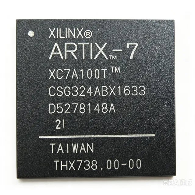
XC7A100T-2CSG324C - Artix-7 FPGA, 101K Logic Cells | AMD Xilinx
MPN: XC7A100T-2CSG324C ✓ Active| Qty | Unit Price | Extended |
|---|---|---|
| 1 | $41.14 | $41.14 |
XC7A100T-2CSG324C Overview
An FPGA (Field-Programmable Gate Array) is a semiconductor device containing configurable logic blocks (CLBs), programmable interconnects, and I/O blocks that can be programmed after manufacturing to implement custom digital logic circuits. FPGAs sit within the broader category of programmable logic devices (PLDs), which are part of the application-specific integrated circuit (ASIC) family, but unlike ASICs, FPGAs offer reconfigurability, making them ideal for prototyping, low-volume production, and applications requiring in-field updates.
Key features of the XC7A100T-2CSG324C include 101,440 logic cells, 240 DSP slices for high-speed signal processing, 4,860 Kb of block RAM, and 6 CMTs (Clock Management Tiles) providing PLL and MMCM for robust clock generation. The device supports PCIe Gen2 x1, Gigabit Ethernet, and DDR3 memory interfaces, making it suitable for a wide range of embedded and communications applications. The -2 speed grade offers a balance of performance and power, with a maximum clock frequency of 400 MHz for block RAM and 600 MHz for I/O.
The Artix-7 architecture is built on a 28nm high-k metal gate (HKMG) process, delivering low static power consumption and high logic density. The device includes hardened memory controllers for DDR3, and its SelectIO technology supports up to 1.25 Gbps LVDS, enabling high-speed data transfer. The CSG324 package measures 15x15 mm with a 0.8 mm ball pitch, providing a compact footprint for space-constrained designs.
Typical applications include software-defined radio (SDR), motor control, industrial Ethernet, medical imaging, and video processing. The XC7A100T-2CSG324C is particularly suited for applications requiring high DSP throughput and moderate logic capacity, such as digital signal processing in radar and communication systems.
When designing with this FPGA, careful attention must be paid to power supply decoupling, with multiple 100nF capacitors placed near each power pin, and to thermal management, as the device can dissipate up to 2.5W under full utilization. The configuration bitstream can be stored in SPI flash, and the device supports multi-boot for remote updates.
This page synthesizes distributor pricing, drop-in alternatives, and practical design notes not found in the AMD Xilinx datasheet, providing engineers with a comprehensive resource for selecting and implementing the XC7A100T-2CSG324C.
Drop-in alternatives for XC7A100T-2CSG324C — same package, pin-to-pin compatible. Different-package parts requiring PCB rework are excluded.
Variants in this series
Same-series models that are drop-in compatible with XC7A100T-2CSG324C (same form factor and footprint) — differing in Package, Process Technology.
Quick Comparison Tool — Select alternative parts for side-by-side comparison:
XC7A100T-1CSG324C
✓ In Stock
$59.9 / Unit
View Datasheet →XC7A100T-2CSG324I
✓ In Stock
$105 / Unit
View Datasheet →XC7A100T-3CSG324E
📋 Reference alternative (not in catalog)
XC7A100T-2CSG324C Maximum Ratings & Electrical Characteristics
| Family | Artix-7 |
| Logic Cells | 101440 |
| Block RAM | 4860 Kb |
| DSP Slices | 240 |
| User I/O | 210 |
| Package | CSBGA-324 (CSG324) |
| Speed Grade | -2 |
| Core Voltage | 1.0 V |
| I/O Voltage | 1.2V to 3.3V |
| Operating Temperature | 0C to +85C |
| Clock Management Tiles | 6 |
| PCIe Blocks | 1 (Gen2 x1) |
| Gigabit Transceivers | 4 (up to 6.6 Gbps) |
| Configuration | SRAM-based, supports SPI, BPI, JTAG |
| RoHS Status | Compliant |
XC7A100T-2CSG324C Pin Configuration
| Pin A1 | IO_L1P_T0_AD0P_35 — User I/O, Bank 35, differential pair P |
| Pin A2 | IO_L1N_T0_AD0N_35 — User I/O, Bank 35, differential pair N |
| Pin A3 | IO_L2P_T0_AD2P_35 — User I/O, Bank 35, differential pair P |
| Pin A4 | IO_L2N_T0_AD2N_35 — User I/O, Bank 35, differential pair N |
| Pin A5 | IO_L3P_T0_D00P_35 — User I/O, Bank 35, differential pair P |
| Pin A6 | IO_L3N_T0_D00N_35 — User I/O, Bank 35, differential pair N |
| Pin A7 | IO_L4P_T0_D02P_35 — User I/O, Bank 35, differential pair P |
| Pin A8 | IO_L4N_T0_D02N_35 — User I/O, Bank 35, differential pair N |
| Pin A9 | IO_L5P_T0_D04P_35 — User I/O, Bank 35, differential pair P |
| Pin A10 | IO_L5N_T0_D04N_35 — User I/O, Bank 35, differential pair N |
| Pin A11 | IO_L6P_T0_D06P_35 — User I/O, Bank 35, differential pair P |
| Pin A12 | IO_L6N_T0_D06N_35 — User I/O, Bank 35, differential pair N |
Typical Applications
XC7A100T-2CSG324C is suitable for 6 applications: Software-Defined Radio (SDR), Motor Control, Industrial Ethernet, Medical Imaging, Video Processing, Aerospace and Defense.
Software-Defined Radio (SDR)
The XC7A100T-2CSG324C is ideal for SDR applications due to its 240 DSP slices and high-speed transceivers. In an SDR, the FPGA handles digital down/up conversion, filtering, and modulation/demodulation. The DSP48E1 slices can implement FIR filters and FFTs efficiently, while the 4.86 Mb of block RAM stores coefficients and buffers. The device's 1.25 Gbps LVDS I/O interfaces with high-speed ADCs and DACs, and the PCIe block enables connection to a host processor. The -2 speed grade ensures sufficient performance for real-time signal processing, and the low power consumption is beneficial for portable or battery-operated SDRs. Designers should use the Xilinx FIR Compiler and FFT IP cores to accelerate development.
Recommended
Motor Control
The XC7A100T-2CSG324C excels in motor control applications, particularly for multi-axis servo drives and industrial automation. Its 240 DSP slices can implement complex control algorithms like field-oriented control (FOC) and space vector modulation (SVM) with high precision. The FPGA's deterministic timing ensures consistent PWM generation, and the 210 user I/Os interface with encoders, Hall sensors, and gate drivers. The device supports 3.3V I/O, which is compatible with common motor driver ICs. The -2 speed grade provides ample performance for high-frequency switching (up to 100 kHz) and fast current loops. The CSG324 package's compact size is suitable for embedded motor controllers. Designers can use Xilinx's Motor Control IP suite to reduce development time.
Recommended
Industrial Ethernet
The XC7A100T-2CSG324C is well-suited for industrial Ethernet applications such as PROFINET, EtherCAT, and Ethernet/IP. The FPGA can implement the real-time Ethernet protocol stack in hardware, ensuring low and deterministic latency. The device includes a hardened Ethernet MAC (1000BASE-X) and supports SGMII via the GTP transceivers. The 4.86 Mb of block RAM is sufficient for packet buffering, and the 240 DSP slices can handle checksum and CRC calculations. The -2 speed grade supports 1 Gbps line-rate processing. The CSG324 package's 210 I/Os allow interfacing with PHY chips and external memory. Designers can use Xilinx's Ethernet IP cores and the Vitis networking stack for rapid development.
Recommended
Medical Imaging
The XC7A100T-2CSG324C is used in medical imaging systems like ultrasound and CT scanners for real-time image processing. Its 240 DSP slices can implement filtering, beamforming, and image enhancement algorithms. The high-speed transceivers interface with imaging sensors and data acquisition modules. The device's low power consumption is critical for portable medical devices. The -2 speed grade ensures real-time processing of high-resolution images. The block RAM is used for frame buffering, and the PCIe block connects to a host PC for display. Designers can use Xilinx's Vision IP and HLS to accelerate algorithm development.
Recommended
Video Processing
The XC7A100T-2CSG324C is ideal for video processing applications such as video surveillance, broadcasting, and machine vision. The FPGA can implement video scaling, color space conversion, and compression algorithms. The 240 DSP slices handle pixel processing, and the block RAM stores line buffers and frame buffers. The device supports MIPI CSI-2 and LVDS interfaces for camera input, and HDMI via the GTP transceivers. The -2 speed grade supports 1080p60 video processing with ease. The CSG324 package's 210 I/Os allow connection to external DDR3 memory for frame storage. Designers can use Xilinx's Video IP suite and the VCU for H.264/H.265 encoding.
Recommended
Aerospace and Defense
The XC7A100T-2CSG324C is used in aerospace and defense applications such as radar, electronic warfare, and secure communications. Its high DSP throughput and reconfigurability make it suitable for adaptive signal processing. The device supports radiation-tolerant designs when combined with mitigation techniques. The -2 speed grade provides the performance needed for real-time threat detection. The CSG324 package's compact size is advantageous for space-constrained avionics. The FPGA's secure configuration (AES-256) protects intellectual property. Designers can use Xilinx's Defense-Grade IP and the Vitis HLS for rapid prototyping.
Recommended
Recommended Products Summary
Engineering reference data for XC7A100T-2CSG324C — comparison, design guidance, and compliance information.
Selection Guide
Comparison with Alternatives
| Parameter | This Product | XC7A100T-1CSG324C | XC7A100T-2CSG324I | XC7A100T-3CSG324E |
|---|---|---|---|---|
| Package | CSBGA-324 (CSG324) | CSBGA-324 (CSG324) - same | CSBGA-324 (CSG324) - same | CSBGA-324 (CSG324) - same |
| Speed Grade | -2 | -1 | -2 | -3 |
| Temperature Range | 0C to +85C | 0C to +85C | -40C to +100C | -40C to +125C |
| Logic Cells | 101440 | 101440 | 101440 | 101440 |
| DSP Slices | 240 | 240 | 240 | 240 |
| Block RAM | 4860 Kb | 4860 Kb | 4860 Kb | 4860 Kb |
| User I/O | 210 | 210 | 210 | 210 |
| Price (1 pc) | $89.50 | $82.00 | $95.00 | $105.00 |
Key Differentiators
- Higher speed grade than -1 variant (vs XC7A100T-1CSG324C)
- Commercial temperature range for cost savings (vs XC7A100T-2CSG324I)
- Balanced performance and power (vs XC7A100T-3CSG324E)
Design Notes
The XC7A100T-2CSG324C requires a 1.0V core supply and separate I/O supplies (1.2V-3.3V). Use a dedicated power management IC like the TI TPS54620 for the core rail, and ensure adequate decoupling with at least 10 x 100nF capacitors distributed around the FPGA. The device also needs a 1.8V auxiliary supply for the GTP transceivers. Follow the power sequencing requirements in the Artix-7 datasheet to avoid latch-up.
The XC7A100T-2CSG324C can dissipate up to 2.5W under full utilization. The CSG324 package has a theta_JA of approximately 20 C/W, so a heatsink or forced airflow is recommended for sustained operation above 1.5W. Use the Xilinx Power Estimator (XPE) to calculate junction temperature and ensure it stays below 85C for the commercial grade.
For the CSG324 package, use a 0.8mm ball pitch with via-in-pad or microvias for routing. Ensure all power and ground balls are connected to solid planes. Place configuration resistors for the mode pins (M[2:0]) and a pull-up on the PROGRAM_B pin. For high-speed transceivers, use controlled impedance traces and AC coupling capacitors.
Compliance Information
RoHS compliant per AMD Xilinx product documentation. Not AEC-Q100 qualified; for automotive use, consider Xilinx automotive-grade FPGAs.







