FPGA & CPLD
Products (6352)
A3P600-FG144 - 600K Gate Flash FPGA | Microchip Technology
The Microchip Technology A3P600-FG144 is a flash-based Field Programmable Gate Array (FPGA) from the ProASIC3 family, offering 600,000 system gates, 231 MHz maximum internal frequency, and 97 user I/Os in a 144-ball FBGA package. It operates from a 1.5V core supply and is built on a 130-nm, 7-layer metal (6 copper) flash-based CMOS process, providing instant-on, low-power, and secure non-volatile operation. An FPGA (Field Programmable Gate Array) is an integrated circuit that can be configured by the customer after manufacturing to implement custom digital logic functions. FPGAs belong to the broader category of programmable logic devices (PLDs), which sit between fixed-function ASICs and general-purpose processors in the digital logic hierarchy. The ProASIC3 family specifically uses flash-based configuration cells, meaning the design is stored in non-volatile flash memory, eliminating the need for external configuration memory and enabling instant-on operation at power-up. Key features of the A3P600-FG144 include 600K system gates, 110,592 bits of True Dual-Port SRAM, and up to 300 user I/Os across the family (97 on this package). It supports multiple I/O standards including LVCMOS, LVTTL, PCI, and LVDS, with four I/O banks that have dedicated supply voltages. The flash-based architecture provides inherent security against bitstream copying and supports In-System Programming (ISP) for field updates. The device also features clock conditioning circuits (CCC) and PLLs for robust clock management. Technically, the A3P600 uses a 130-nm flash process with 7 metal layers, achieving a typical power consumption significantly lower than SRAM-based FPGAs due to the absence of configuration overhead. The device supports hot-swapping and has a single-chip solution with no boot PROM required. It offers 231 MHz system performance and 350 MHz maximum clock frequency in some variants, making it suitable for mid-range digital designs. Typical applications include industrial control, automotive electronics, communications infrastructure, and consumer electronics where low power, instant-on, and security are critical. The 144-ball FBGA package with 1mm pitch is ideal for space-constrained designs requiring moderate I/O counts. When designing with this device, ensure proper decoupling of the 1.5V core supply and each VCCIBx bank supply. The flash-based configuration retains the design even without power, but careful power sequencing is recommended to avoid I/O contention during power-up. This page synthesizes distributor pricing, drop-in alternatives, and practical design notes not found in the manufacturer datasheet, providing a comprehensive resource for engineers evaluating the A3P600-FG144.
A3P600-FG144I - 600K Gate ProASIC3 FPGA | Microchip
The Microchip Technology A3P600-FG144I is a flash-based FPGA from the ProASIC3 family, offering 600,000 system gates, 13,824 logic elements (CLBs), and a maximum operating frequency of 350 MHz. It is housed in a 144-ball FBGA package with 1 mm pitch, providing 97 user I/Os. This device operates from a 1.5V core supply and supports an industrial temperature range of -40°C to +100°C, making it suitable for demanding embedded applications. A Field-Programmable Gate Array (FPGA) is an integrated circuit that can be configured by the customer after manufacturing to implement custom digital logic functions. Unlike fixed-function ASICs, FPGAs offer reconfigurability, allowing designers to iterate on designs without the cost and lead time of custom silicon. The ProASIC3 family is part of the broader FPGA category, which also includes SRAM-based FPGAs from competitors like Xilinx and Intel. Flash-based FPGAs like the A3P600 retain their configuration even when power is removed, providing instant-on capability and enhanced security against reverse engineering. Key features of the A3P600-FG144I include its flash-based non-volatile configuration, which eliminates the need for external boot memory and reduces system complexity. It offers 600,000 system gates, 13,824 CLBs, and 97 user I/Os, with support for multiple I/O standards including LVCMOS, LVTTL, and PCI. The device also includes up to 108 Kbits of embedded RAM, PLLs for clock management, and a secure programming mode. Its low power consumption and single-chip solution make it ideal for cost-sensitive applications. From a technical perspective, the A3P600 is built on a 130 nm flash process, providing a balance of performance and power efficiency. The flash-based architecture allows for live updates and secure in-system programming, which is critical for field-upgradeable systems. The device supports JTAG (IEEE 1149.1) for boundary-scan testing and programming, and it is compatible with Microchip's Libero SoC design suite, which includes synthesis, simulation, and place-and-route tools. Typical applications for the A3P600-FG144I include industrial control systems, automotive electronics, communications infrastructure, and aerospace/defense systems. Its instant-on capability and high reliability make it well-suited for safety-critical applications where immediate operation is required after power-up. The 97 I/Os and 144-ball package allow for compact PCB designs with moderate pin count requirements. When designing with this FPGA, consider the 1.5V core supply and ensure adequate decoupling capacitors are placed near the power pins. The device supports multiple I/O banks with independent voltage supplies, enabling mixed-voltage systems. For high-speed designs, pay attention to signal integrity and use the on-chip PLLs to generate clean clock signals. This page synthesizes distributor pricing, drop-in alternatives, and practical design notes not found in the manufacturer datasheet, providing a comprehensive resource for engineers evaluating the A3P600-FG144I.

A3P600-FG256I - ProASIC3 FPGA, 600K Gates | Microchip Technology
The Microchip Technology A3P600-FG256I is a ProASIC3 flash-based Field Programmable Gate Array (FPGA) with 600K system gates, 13,824 VersaTiles (approximately 7K logic elements), 177 user I/O, and 110,592 RAM bits, supplied in a 256-pin FBGA (LBGA-256) package. It operates from a 1.5 V core supply, enabling single-chip, reprogrammable logic for mid-density industrial and communications applications. What is a Field Programmable Gate Array? An FPGA is a semiconductor device containing configurable logic blocks and programmable interconnects that can be reconfigured after manufacturing to implement arbitrary digital logic. Unlike fixed-function ASICs, FPGAs allow in-system design changes and rapid prototyping. Microchip's ProASIC3 family uses nonvolatile flash-based configuration, meaning the FPGA retains its programming without an external boot PROM while still being reprogrammable. The A3P600-FG256I sits in the FPGA -> programmable logic -> integrated circuit hierarchy and is often selected for applications requiring secure IP protection, flexible I/O, and low total cost of ownership. Key features of the A3P600-FG256I include 600K system gates, 13,824 VersaTiles, 177 user I/O, 110,592 RAM bits, a 1.5 V core supply, and a 17 x 17 mm 256-ball FBGA package with 1 mm pitch. The flash-based architecture provides nonvolatile configuration, in-system programmability, and a small footprint for mid-density logic designs. According to Mouser, the device is categorized as a 7KLEs ProASIC3 FPGA, and DigiKey confirms the 177 I/O and 110,592 RAM bit organization. Technically, the ProASIC3 architecture uses a proprietary VersaTile structure that can be configured as a three-input lookup table or a D-flip-flop with enable, giving designers efficient implementation of combinational and sequential logic. The 256-LBGA package balances I/O count and board area while offering a standard 1.5 V core voltage. The device is in-system programmable, and its flash configuration simplifies power-up sequencing because no external configuration device is required. Arrow lists the device as a 600K-gate FPGA with 231 MHz system performance, while other listings cite 350 MHz; designers should verify the exact speed grade against the latest datasheet. Typical applications for the A3P600-FG256I include industrial automation, motor control, wired communications, medical device signal processing, and IoT edge gateways. Its 177 user I/O and 110K-bit embedded RAM support bus interfaces, state machines, and digital signal processing functions. The industrial temperature suffix (I) makes it suitable for harsh operating environments. The flash-based architecture also reduces system cost by eliminating external PROMs and simplifies field updates. When designing with the A3P600-FG256I, pay careful attention to power supply decoupling, BGA thermal management, and I/O bank voltage assignments. Because the device is flash-based, no external configuration device is required, which saves board space and reduces boot time. Sufficient VCC and ground plane stitching under the 256-ball package is essential for reliable operation, especially at higher I/O toggle rates. This page synthesizes distributor pricing, drop-in package variants, practical design notes, a comparison table, and AEO-optimized FAQ content that goes beyond the raw manufacturer datasheet. It is intended to help engineers quickly evaluate the A3P600-FG256I against other ProASIC3 family members and make a confident selection for new designs.
A3P600-FG484 - ProASIC3 600K-Gate Flash FPGA, 484-BGA | Microchip
The Microchip (Microsemi) A3P600-FG484 is a 600,000-gate ProASIC3 flash-based FPGA with up to 235 user I/Os, a 231 MHz system performance rating, and 130 nm 7-layer metal flash process technology, housed in a 484-pin Fine-Pitch Ball Grid Array (FBGA, 23x23 mm) operating at a 1.5 V core supply. A flash-based FPGA stores its configuration in on-chip flash cells rather than the SRAM lookup tables used by Xilinx or Intel (Altera) devices. Because configuration is non-volatile, the A3P600 powers up instantly with no external boot PROM, no configuration controller, and no bitstream exposure during power-up - a major advantage for security-sensitive and high-reliability systems. In the programmable logic hierarchy, the A3P600 sits in the mid-density tier of the ProASIC3 family, above the A3P250 and below the A3P1000. Key features include single-chip, single-voltage operation (1.425 V to 1.575 V core), support for optional soft ARM Cortex-M1 processor cores, abundant 18-kbit embedded block SRAM, and reprogrammability without a separate configuration device. The flash fabric also delivers inherently low static power and better SEU robustness than SRAM-based competitors. Architecturally, the device is built from VersaTiles - a fine-grained logic tile that can act as a three-input LUT, a D-flip-flop, or a latch with enable - interconnected by segmented routing. Clock resources support multiple PLLs and clock-conditioning circuits for source-synchronous interfaces up to 231 MHz. Typical applications include industrial automation controllers, medical instrumentation, military/aerospace subsystems (where the related RTAX radiation-tolerant family is used), communications bridging, and secure embedded systems requiring instant-on, tamper-resistant configuration storage. Design consideration: the 484-FBGA requires careful power-plane design at 1.5 V and attention to simultaneously switching output (SSO) limits; consult the Microchip ProASIC3/E SSO and Pin Placement Guidelines when assigning high-drive I/O banks. This page synthesizes distributor pricing, drop-in same-footprint alternatives, design notes, and AEO-optimized FAQs not consolidated in the manufacturer datasheet.
A3P600-FG484I - 600K Gate Flash FPGA, 231MHz | Microchip
The Microchip A3P600-FG484I is a flash-based FPGA from the ProASIC®3 family, offering 600K system gates, a maximum operating frequency of 231MHz, and 235 user I/Os in a 484-pin FBGA package. It operates from a 1.5V core supply and is built on 130nm flash technology, providing a single-chip, reprogrammable solution with instant-on capability and inherent security. An FPGA (Field Programmable Gate Array) is an integrated circuit that can be configured by the customer after manufacturing to implement arbitrary digital logic functions. Unlike microcontrollers or ASICs, FPGAs contain a fabric of programmable logic blocks and interconnects, allowing designers to create custom hardware without the cost and lead time of a custom chip. The ProASIC3 family uses flash-based configuration cells, which retain their programming even when power is removed, enabling instant-on operation and eliminating the need for external boot memory. Key features of the A3P600-FG484I include 600K system gates, 231MHz system performance, 235 user I/Os, and 1.5V core operation. The flash-based architecture provides non-volatile configuration, low power consumption, and high security against reverse engineering. The device supports up to 128K bits of flash memory for user data and includes advanced clock management with up to 6 PLLs, enabling robust timing control for complex designs. The ProASIC3 architecture uses a VersaTile core that can be configured as either a three-input lookup table (LUT) or a D-flip-flop/latch with enable, providing efficient use of the FPGA fabric. The 130nm flash process delivers a balance of performance and power, with low static power consumption ideal for battery-powered and thermally constrained applications. The device supports multiple I/O standards including LVCMOS, LVTTL, and differential standards, offering design flexibility. Typical applications for the A3P600-FG484I include industrial control, automotive electronics, communications infrastructure, and aerospace systems where reliability, security, and instant-on operation are critical. Its non-volatile configuration makes it suitable for safety-critical applications that require immediate functionality upon power-up without external configuration devices. When designing with this device, consider the 1.5V core supply requirement and ensure adequate decoupling on all power pins. The flash-based configuration eliminates the need for a configuration PROM, simplifying board design and reducing BOM cost. For high-speed I/O, follow the manufacturer's layout guidelines for signal integrity and use the integrated PLLs for clock management. This page synthesizes distributor pricing, drop-in alternatives, and practical design notes not found in the manufacturer datasheet, providing engineers with a comprehensive resource for evaluating the A3P600-FG484I in their designs.
A3P600-FGG144 - 600K-Gate ProASIC3 Flash FPGA | Microchip
The Microchip Technology A3P600-FGG144 is a 600,000-gate ProASIC3 flash-based FPGA with 97 user I/Os, 13,824 CLBs, and 110592 bits of configuration flash memory, housed in a 144-ball Fine-Pitch Ball Grid Array (FBGA/LBGA) package. As a member of the third-generation ProASIC3 family originally developed by Actel and now part of Microchip, it delivers ASIC-level integration with a single-chip, nonvolatile, Instant-On solution. A flash-based FPGA (field-programmable gate array) stores its configuration in on-chip flash cells rather than SRAM, eliminating the need for an external boot PROM and greatly improving design security. Within the programmable logic hierarchy, the A3P600 sits in the mid-density tier of the ProASIC3 family, above the A3P250 and below the A3P1000, and belongs to the broader category of programmable logic devices that also includes CPLDs and antifuse FPGAs. Key features include nonvolatile flash programming for a true single-chip solution, reprogrammability with no external configuration device, low total cost of ownership as highlighted by Microchip, and a compact 144-ball footprint with 1.00 mm ball pitch suitable for surface-mount assembly. The device provides 97 usable I/Os distributed across four I/O banks whose VCCIBx supplies are bank-independent, allowing mixed-voltage I/O standards on one package. Architecturally, the ProASIC3 fabric consists of VersaTiles implementing sequential or combinable logic, supported by embedded flash blocks for on-chip nonvolatile storage. Optional soft ARM capability in the family enables embedded processor designs on the same fabric. CMOS flash technology yields low static power versus SRAM FPGAs of similar density. Typical applications include industrial control, motor drive interface logic, bridging and glue logic consolidation, secure single-chip designs where bitstream theft is a concern, and portable or battery-powered systems benefiting from low standby power. Design consideration: assign I/Os bank-aware, since only I/Os with compatible voltage standards may share a VCCIBx bank, per the Microchip migration application note. This page synthesizes distributor pricing, drop-in same-package alternatives from the ProASIC3 family, and practical design notes not found in the manufacturer datasheet.
A3P600-FGG144I - 600K Gate ProASIC3 FPGA | Microchip
The Microchip Technology A3P600-FGG144I is a flash-based field-programmable gate array (FPGA) from the ProASIC3 family, offering 600,000 system gates, 110,592 bits of RAM, and 97 user I/Os in a 144-pin FBGA (FGG144) package. It operates at a core voltage of 1.5V and supports system performance up to 231 MHz, making it suitable for a wide range of low-power, high-reliability applications. A field-programmable gate array (FPGA) is an integrated circuit that can be configured by the customer after manufacturing to implement custom digital logic functions. Unlike fixed-function ASICs, FPGAs offer reprogrammability, rapid prototyping, and lower non-recurring engineering costs. The ProASIC3 family uses flash-based configuration cells, providing non-volatile storage of the design, instant-on capability, and immunity to single-event upsets (SEU) in radiation environments, which is a key advantage over SRAM-based FPGAs that require external configuration memory. Key features of the A3P600-FGG144I include 600K system gates, 110,592 bits of RAM, 97 user I/Os, and support for up to 231 MHz system performance. It operates from a 1.5V core supply and is available in a lead-free, RoHS-compliant 144-pin FBGA package. The device also supports multiple I/O standards, including LVCMOS, LVTTL, and PCI, and includes phase-locked loops (PLLs) for clock management. Its flash-based architecture provides secure, low-power operation with instant-on capability, eliminating the need for external boot memory. Technically, the A3P600-FGG144I is fabricated using a 130nm flash process, which balances performance and power consumption. The device integrates 13,824 logic modules (tiles) and 110,592 bits of RAM, organized as 1,536 words of 72 bits each. It includes up to 3 PLLs and supports various I/O standards. The flash-based configuration cells are reprogrammable, allowing design updates in the field. The device also features advanced security to prevent unauthorized readback, making it suitable for IP protection. Typical applications include industrial automation, automotive electronics, communications infrastructure, and aerospace systems. In industrial automation, the A3P600-FGG144I can implement motor control, sensor interfacing, and real-time processing. In automotive, it supports infotainment, driver assistance, and body control modules. Its low power and instant-on capability make it ideal for battery-powered and safety-critical systems. When designing with this device, ensure proper power supply decoupling with 0.1uF and 10uF capacitors near the VCC and GND pins. The core voltage must be regulated to 1.5V ±5%. For I/O banks, follow the recommended termination and voltage levels for the chosen I/O standard. Use the Microchip Libero SoC design suite for synthesis, place-and-route, and programming. This page synthesizes distributor pricing, drop-in alternatives, and practical design notes not found in the manufacturer datasheet, providing engineers with a comprehensive resource for evaluating the A3P600-FGG144I.
A3P600-FGG256 - 600K Gate ProASIC3 FPGA | Microchip Technology
The Microchip Technology A3P600-FGG256 is a 600,000 system-gate ProASIC3 flash Field Programmable Gate Array (FPGA) with 177 user I/Os, 110,592 total RAM bits, and a maximum system frequency of 231 MHz, housed in a 256-ball FBGA (17x17 mm) package. This single-chip, instant-on FPGA operates from a 1.5V core supply and supports commercial temperature operation from 0°C to 85°C. A Field Programmable Gate Array (FPGA) is a semiconductor device containing configurable logic blocks and programmable interconnects that can be configured after manufacturing to implement arbitrary digital logic. In the programmable logic taxonomy, FPGA sits within the broader family of programmable logic devices; ProASIC3 is Microchip's flash-based FPGA family. Unlike SRAM-based FPGAs, ProASIC3 stores its configuration in nonvolatile flash cells, enabling instant-on operation without external boot memory. This architecture improves system reliability, reduces bill-of-materials count, and provides inherent bitstream security. Key features of the A3P600-FGG256 include nonvolatile flash configuration with instant-on capability, 600K system gates, 177 user I/Os, 110,592 RAM bits, 231 MHz system performance, and a 1.425V-1.575V supply range. The device is RoHS3 compliant and lead-free, and it is supplied in a 256-FPBGA package with a 17x17 mm body and 1.00 mm ball pitch. The four I/O banks with dedicated VCCIB supplies allow flexible voltage-standard mixing on the same device. The ProASIC3 family is built on a flash-based CMOS process, combining ASIC-like unit cost with full reprogrammability. The device integrates dedicated clock conditioning PLLs and embedded memory resources. According to Microchip's ProASIC3 migration application note, A3P400, A3P600, and A3P1000 devices share four I/O banks and dedicated bank supplies, which simplifies board design when moving between densities in the same 256-ball package. The flash architecture also provides design security and low dynamic power density. Typical applications include industrial automation and motor control, communications protocol bridging, medical signal processing, aerospace and defense secure processing, smart energy monitoring, and ASIC replacement. The 177 user I/Os and instant-on behavior make the A3P600-FGG256 suitable for high-reliability systems where external configuration devices are undesirable or where fast startup is critical. When designing with this FPGA, pay careful attention to 1.5V core supply decoupling and to each I/O bank's VCCIB voltage. Use Microchip's power management guidelines, and verify pin compatibility when migrating between ProASIC3 densities using the same 256-FPBGA footprint. For industrial-temperature environments, select the A3P600-FGG256I variant. This page synthesizes distributor inventory, estimated pricing, drop-in alternatives from the same ProASIC3 family, and practical design notes not found in the manufacturer datasheet, giving engineers a complete cross-reference resource for the A3P600-FGG256.
A3P600-FGG256I - ProASIC3 Flash FPGA 600K Gates | Microchip
The Microchip Technology (formerly Microsemi/Actel) A3P600-FGG256I is a 600K-system-gate ProASIC3 flash-based FPGA with 13,824 registers, 110,592 bits of embedded RAM, 177 user I/Os, and a maximum system performance of 231 MHz, fabricated on a 130nm process and housed in a 256-ball Fine-Pitch Ball Grid Array (FBGA) package rated for the industrial temperature range of -40C to +85C. A flash-based FPGA is a field-programmable gate array whose configuration is stored in on-chip flash memory cells rather than SRAM, allowing single-chip, instant-on operation without an external configuration device. Within the programmable logic hierarchy, the A3P600 sits in the mid-density tier of the ProASIC3 family, above the A3P400 and below the A3P1000. Key features include nonvolatile flash programming that eliminates the boot-time and security exposure of SRAM FPGAs, four I/O banks with independently configurable VCCIBx supplies supporting mixed-voltage systems, 1.5V core operation for low dynamic power, and reprogrammability for in-field updates. Low total cost of ownership (TOC) is a stated family pillar on the Microchip product page. Architecturally, ProASIC3 uses a sea-of-gates fabric of versatile logic elements and embedded flash switches, delivering deterministic, ASIC-like security because the bitstream is stored invisibly in flash and cannot be read back. The 130nm process balances density, cost, and power, while the 231 MHz ceiling supports real-time signal processing and glue-logic consolidation. Typical applications include industrial automation controllers, communications line cards, real-time signal processing, custom hardware acceleration, and secure single-chip logic replacement in aerospace-adjacent industrial systems, where instant-on startup and configuration security are decisive. A key design consideration: assign I/O standards with compatible voltage levels to the same VCCIBx bank, because bank supplies are dedicated and cannot be mixed within a bank, per Microchip migration application notes. This page synthesizes distributor pricing, drop-in alternatives, and practical design notes not found in the manufacturer datasheet, providing information gain for engineers evaluating the ProASIC3 family.
A3P600-FGG484 - 600K Gate ProASIC3 FPGA | Microchip
The Microchip (Microsemi) A3P600-FGG484 is a flash-based ProASIC3 family FPGA with 600K system gates, a system performance of 231 MHz, and 235 user I/Os, housed in a 484-ball Fine-Pitch Ball Grid Array (FBGA) package and operating from a 1.5V core supply on a 130nm process. A field-programmable gate array (FPGA) is a semiconductor device containing a fabric of configurable logic blocks, routing resources, and I/O cells that designers program to implement custom digital circuits. Unlike SRAM-based FPGAs, the ProASIC3 family uses flash-based configuration cells, meaning the device is non-volatile, single-chip (no external boot configuration device is required), and instant-on at power-up. Within the programmable logic hierarchy, the A3P600 sits between the smaller A3P400 and the larger A3P1000 in the ProASIC3 family. Key differentiating specifications include 600K system gates in the ProASIC3 fabric, 235 user I/Os on the 484-pin FBGA, a maximum system frequency of 231 MHz, and support for embedded soft processors in the Microchip/Microsemi tool flow. The flash-based fabric delivers low total cost of ownership by eliminating the external configuration flash, reducing bill-of-materials cost and board area while improving system security because the bitstream is stored on-chip. Technically, the A3P600 is built on a 130nm CMOS process with a 1.5V core. The VersaTile-based architecture allows each tile to be used as a lookup table, flip-flop, or embedded memory element, giving designers fine-grained flexibility. On-chip flash and RAM blocks support FIFOs and buffering in data-path designs. Typical applications include industrial control and automation, medical instrumentation, military and aerospace subsystems (in industrial temperature variants), communication bridging, and secure single-chip logic integration where instant-on operation is required. Design consideration: plan I/O banking and power supply sequencing early, as the FBGA package limits rework options; verify availability of the non-automotive commercial temperature grade before finalizing sourcing. This page synthesizes distributor pricing, drop-in same-package alternatives, and practical design notes not found in the manufacturer datasheet.
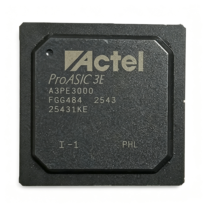
A3P600-FGG484I - 600K Gate Flash FPGA, 231MHz | Microchip
The Microchip Technology A3P600-FGG484I is a ProASIC3 flash-based field programmable gate array (FPGA) with 600,000 system gates, 231 MHz system performance, and a 1.5 V core, housed in a 484-pin FBGA (FGG) package. The industrial-temperature (I) variant supports demanding operating environments, and the lead-free finish meets modern assembly requirements. With 235 user I/O and 13.5 kB of embedded SRAM, this device provides a balanced mix of logic density, I/O capability, and non-volatile configuration. A field programmable gate array (FPGA) is a semiconductor device containing programmable logic blocks and programmable interconnect that can be configured after manufacturing to implement custom digital logic. The A3P600-FGG484I belongs to the ProASIC3 family, which uses flash-based configuration cells instead of SRAM. This places it within the broader FPGA hierarchy: flash FPGA -> ProASIC3 family -> Microchip programmable logic portfolio. Because configuration is stored in non-volatile flash, the device is instantly live on power-up, requires no external boot PROM, and resists unauthorized readback, making it suitable for secure and mission-critical systems. Key features of the A3P600-FGG484I include 600K system gates, 235 user I/O, 13.5 kB SRAM, 231 MHz system performance, and a 1.5 V core supply. The flash-based architecture provides instant-on operation, low power, and single-chip security. The FGG484 package is a lead-free 484-ball fine-pitch ball grid array, and the industrial temperature grade supports applications from -40C to +100C (per Microchip's standard industrial-grade definition). The device is programmable through a standard JTAG interface and can be reprogrammed in-system for prototyping or field updates. The ProASIC3 architecture uses 130 nm flash technology, balancing density, performance, and cost. Since configuration is stored on-chip, external configuration memory is eliminated, reducing BOM cost and board space while improving security. The device supports multiple I/O standards, enabling direct interface to LVCMOS, LVTTL, and other common logic families. The 13.5 kB SRAM can be used for FIFOs, small buffers, or scratchpad memory in soft-processor and state-machine designs, and the 231 MHz system performance is adequate for many industrial, communications, and display processing tasks. Typical applications include industrial motor control, avionics display processing, medical monitoring, communications protocol bridging, and IoT edge aggregation. The instant-on behavior and secure flash configuration make the A3P600-FGG484I a strong choice for security-conscious designs such as encrypted communication modules and tamper-resistant control systems. The 235 I/O pins support parallel data buses, memory interfaces, and high-density sensor arrays, and the 1.5 V core reduces power consumption compared to older 3.3 V FPGAs. When designing with the A3P600-FGG484I, pay attention to power-supply decoupling and I/O bank planning. Place 100 nF ceramic capacitors close to each power/ground ball pair and use bulk capacitance on the 1.5 V core rail. Verify that each I/O bank voltage is connected to the correct external supply before configuration, and leave unused I/O in a defined state. Because the device is flash-based, no configuration device is required, but a JTAG header is recommended for programming and debug. Follow Microchip's PCB layout guidance for the 484-ball FBGA to ensure reliable solder joints and thermal performance. This page synthesizes distributor pricing, same-family drop-in alternatives, and practical design notes not found in the manufacturer datasheet, helping engineers select, validate, and replace the A3P600-FGG484I with confidence.
A3P600-PQG208 - 600K-Gate ProASIC3 Flash FPGA | Microchip
The Microchip Technology A3P600-PQG208 is a 600,000-gate ProASIC3 flash-based FPGA with 7K logic elements (13,824 VersaTiles), 154 user I/Os, and 231 MHz system performance, housed in a 208-pin PQFP (PQG208) package operating from a 1.5V core supply. It is a single-chip, reprogrammable, non-volatile FPGA fabricated on a 130nm flash process. A flash FPGA is a field-programmable gate array whose configuration is stored in on-chip flash memory cells rather than an external configuration ROM. This places it in the power-management hierarchy of programmable logic: FPGA -> flash FPGA -> single-chip programmable SoC solution. Because configuration data is non-volatile, the A3P600 powers up instantly with no external boot device, reducing bill-of-materials cost, board area, and configuration-time attack surface. Key features include single-chip operation with on-chip flash, low total cost of ownership, wide-range I/O supporting the JESD8-B specification for 3V and 3.3V supplies, 110,592 bits of distributed resources, and reprogrammability for field upgrades. The VersaTile architecture lets each tile act as a three-input LUT, a D-flip-flop with enable, or a latch, improving fabric utilization versus pure LUT architectures. Architecturally, the ProASIC3 core tile combines VersaTiles with embedded flash blocks and clock-conditioning circuitry. The 130nm flash process yields instant-on, high-security, low-power operation suited to sense-and-control systems where reliability, security, and power matter. Typical applications include industrial automation and motor control, aerospace and defense secure logic, medical instrumentation, communications line cards, and power sequencing/glue logic replacing multiple ASICs or ASSPs. A key design consideration is I/O bank planning: the wide-range I/O eases bank management, but designers must still verify voltage domains and toggle-rate-driven power per the datasheet guidelines. This page adds value beyond the datasheet by synthesizing distributor pricing, drop-in alternatives within the ProASIC3 PQ208 family, and practical design notes in one place.
A3P600-PQG208I - ProASIC3 Flash FPGA 600K Gates | Microchip
The Microchip (Microsemi) A3P600-PQG208I is a ProASIC3 family flash-based FPGA delivering 600K system gates with 154 user I/Os in a 208-pin PQFP (BFQFP) package, operating from a 1.5V core supply at up to 231 MHz system performance in the industrial (-40C to +100C, junction) temperature range. A flash-based FPGA is a field-programmable gate array whose configuration is stored in on-chip non-volatile flash memory rather than an external configuration ROM. Within the programmable logic hierarchy (FPGA -> programmable logic device -> digital logic IC -> semiconductor), flash FPGAs occupy the single-chip, instant-on niche: they power up live without a boot sequence and are inherently secure because the bitstream never leaves the device. Key features include single-chip operation with no external configuration device, reprogrammable flash fabric built on a 130nm process, 7K-class logic elements per distributor listings, and support for soft ARM processor cores per the ProASIC3 family datasheet. The fabric uses an 8-input versatile lookup table architecture that provides high effective logic density, and embedded memory blocks support FIFOs and dual-port RAM implementations. Architecturally, ProASIC3 combines the low static power and high logic utilization of the Actel-originated flash fabric with 1.5V core operation, advanced I/O standards including LVTTL, LVCMOS, SSTL, and differential standards such as LVDS, and hot-swap capable I/Os. Clock conditioning and PLL resources support the 231 MHz system performance figure cited in market data. Typical applications include industrial control and automation, space-constrained secure systems, avionics glue logic consolidation, motor drive interfaces, and communications bridging, where instant-on and single-chip configuration security matter more than raw gate count. Design consideration: verify I/O bank voltage assignment early - each bank must share a compatible VCCI standard, and the PQFP thermal pad requires standard JEDEC footprint copper for dissipation at high toggle rates. This page synthesizes distributor pricing, drop-in same-package family alternatives, and practical design notes not consolidated in the manufacturer datasheet.
A3P600L-1FG144 - 600K-Gate ProASIC3L Flash FPGA | Microchip
The Microchip Technology (Microsemi) A3P600L-1FG144 is a low-power ProASIC3L flash-based FPGA with 600K system gates, 97 user I/Os, and a 1.2 V core voltage, housed in a 144-ball Fine-Pitch Ball Grid Array (FBGA/FG144) package. A flash-based FPGA is a field programmable gate array whose configuration data is stored in on-chip flash memory rather than an external configuration device. Within the programmable logic hierarchy, the ProASIC3L belongs to the FPGA -> programmable logic IC -> semiconductor taxonomy. Because the configuration is nonvolatile, the device powers up instantly with single-chip operation, requiring no boot PROM and offering inherent resistance to configuration readback (SEU-tolerant by architecture). Key features include the low-power 'L' variant optimized for 1.2 V to 1.5 V core operation, 130 nm flash process technology, reprogrammability without an external controller, and abundant advanced features such as embedded block RAM with a total of 110592 bits of configuration/user resources reported by distributors. ProASIC3 offers high performance in ultra-low-density FPGA applications as a single-chip solution with a small footprint. The ProASIC3L fabric uses VersaTile logic elements supporting both combinatorial and sequential logic, combined with embedded SRAM blocks for data buffering. Flash switching elements eliminate the standby configuration power of SRAM-based FPGAs and simplify power sequencing and supply design in space- and power-constrained systems. Typical applications include industrial automation control, portable and battery-powered instrumentation, communications bridging and glue logic, aerospace system controllers, and secure single-chip designs where bitstream volatility is undesirable. Designers should verify speed grade (-1) timing in Microchip Libero SoC and budget I/O banks according to the 97 available user I/Os on the FG144 package. This page synthesizes distributor pricing, drop-in alternatives, and practical design notes not found in the manufacturer datasheet.
A3P600L-1FG144I - ProASIC3L FPGA 600K Gates | Microchip
The Microchip Technology A3P600L-1FG144I is a low-power ProASIC3L family Field Programmable Gate Array (FPGA) featuring 600K system gates, 97 user I/Os, 110592 bits of embedded flash memory-based configuration, and a 1.2 V core supply, housed in a 144-ball Fine-Pitch Ball Grid Array (FBGA/LBGA) package rated for the industrial temperature range. An FPGA (Field-Programmable Gate Array) is a semiconductor device containing a matrix of configurable logic blocks (CLBs) and programmable interconnects that the designer wires together after manufacturing. Within the programmable logic hierarchy, it sits above CPLDs and below high-density FPGA families, providing single-chip system integration without the NRE cost of an ASIC. The ProASIC3L variant of the ProASIC3 family adds a low-power core operating from 1.2 V to 1.5 V for reduced dynamic power consumption. Key differentiating features include flash-based, nonvolatile configuration (no external boot PROM required, instant-on at power-up), a 1.2 V to 1.5 V core voltage for low power operation, and secure, single-chip implementation that resists configuration readback. The 130 nm flash process gives this family inherent radiation tolerance advantages over SRAM FPGAs and eliminates configuration load time. Technically, the device integrates 600K system gates with versatile logic elements, embedded RAM blocks totaling 110592 bits for FIFOs and buffers, and 97 I/Os supporting common single-ended standards with industrial-grade drive. Microchip (formerly Actel/Microsemi) Libero SoC design software supports synthesis, place-and-route, and programming. Typical applications include industrial control, aerospace and defense subsystems, portable and battery-powered instrumentation, communications bridging, and power-sensitive glue-logic consolidation where an SRAM FPGA would consume excessive static power. Design consideration: the 144-FBGA package requires careful ball-mapped PCB layout; verify I/O bank voltage assignments in Libero before routing to avoid bank-conflict errors. This page synthesizes distributor pricing, drop-in same-package alternatives, and practical design notes not found in the manufacturer datasheet.
A3P600L-1FG484 - ProASIC3L FPGA 600K Gates | Microchip
The Microchip Technology (formerly Microsemi) A3P600L-1FG484 is a ProASIC3L low-power flash-based FPGA with 600K system gates, 235 user I/Os, and up to 892.86 MHz performance, fabricated on a 130nm flash process and housed in a 484-pin Fine-Pitch Ball Grid Array (FBGA) package. An FPGA (Field-Programmable Gate Array) is a semiconductor device containing a fabric of configurable logic blocks and programmable interconnects that the designer reconfigures after manufacturing. Within the programmable logic hierarchy, the ProASIC3L sits in the flash-based FPGA class, distinguished from SRAM FPGAs by its non-volatile configuration: the design is stored on-chip, so no external configuration PROM or boot sequence is required, and the device powers up instantly and securely. Key features of the A3P600L-1FG484 include a low-power core operating from 1.2V (the L suffix denotes the low-power core voltage option), a 600K-gate flash fabric with abundant embedded block RAM, 235 available user I/Os for wide bus interfaces, and single-chip operation that reduces total cost of ownership. The 130nm process with flash cells also gives strong security against design cloning compared with bitstream-download SRAM FPGAs. Technically, the ProASIC3L architecture provides VersaTile logic elements that can be configured as combinational logic, D flip-flops, or small memories, plus dedicated embedded memory blocks and optional support for common memory and bus interfaces. The 1.2V core delivers reduced dynamic power, making the device attractive for power-sensitive designs that still need FPGA-scale logic density. Typical applications include industrial automation and motor control glue logic, communications line cards, medical instrumentation, and aerospace-adjacent low-power control systems, where non-volatile, instant-on programmable logic with moderate density is required. When designing with this part, budget power around the 1.2V core rail and verify I/O bank voltage compatibility with adjacent circuitry, and confirm that your CAD flow (Libero SoC) supports the -1 speed grade. This page adds information gain beyond the datasheet by synthesizing distributor stock signals, drop-in alternative options within the ProASIC3L FG484 family, and practical design notes.
A3P600L-1FG484I - ProASIC3L 600K Flash FPGA | Microchip
The Microchip Technology (formerly Microsemi/Actel) A3P600L-1FG484I is a low-power ProASIC3L flash-based FPGA with 600K system gates, 110592 D9 register-cells, up to 235 user I/Os, and a 1.2V core, packaged in a 484-ball Fine-Pitch Ball Grid Array (FG484) industrial-grade (-40C to +100C) variant with speed grade -1. A flash-based FPGA is a field-programmable gate array whose configuration is stored in on-chip non-volatile flash memory rather than an external configuration ROM. In the FPGA hierarchy (FPGA -> programmable logic device -> programmable semiconductor), flash FPGAs occupy the single-chip niche: they power up instantly, require no boot device, and resist configuration corruption, unlike SRAM FPGAs such as Xilinx Spartan or Altera Cyclone families. Key features of the A3P600L include Microchip's Flash*Freeze technology, which dramatically reduces static and dynamic power by allowing near-instant sleep and wake without losing state; a 1.2 V to 1.5 V core voltage range; reprogrammable flash fabric with live-on-power-up operation; and 130 nm flash process technology. The 484-ball FBGA footprint provides ample I/O for bus-wide interfaces while remaining reflow-solderable on standard SMD assembly lines. Architecturally, the ProASIC3L fabric is built from VersaTiles - fine-grained logic tiles that implement both combinational and sequential functions - supported by embedded RAM blocks, FIFO control, and flexible I/O banks supporting multiple voltage standards. Because configuration resides in flash, security against cloning and overbuild is inherently stronger than SRAM-based competitors. Typical applications include portable and battery-powered instrumentation, industrial automation controllers, aerospace sub-systems requiring instant-on logic, communications line cards, and medical monitoring equipment where Flash*Freeze idle current is decisive. Design consideration: budget the power rails per the Microchip power estimator for the -1 speed grade; the Flash*Freeze pin must be properly sequenced with the I/O banks to avoid bus contention during sleep entry and wake-up. This page synthesizes distributor pricing context, same-family drop-in options, and practical design notes not consolidated in the manufacturer datasheet.
A3P600L-1FGG144 - 600K Gate Flash FPGA | Microchip Technology
The Microchip Technology A3P600L-1FGG144 is a low-power flash-based Field Programmable Gate Array (FPGA) from the ProASIC3L family, offering 600,000 system gates, 13,824 logic cells, and 97 user I/Os in a 144-ball FBGA package. It operates with a core voltage of 1.2V to 1.5V and supports a maximum clock frequency of 350MHz, making it suitable for a wide range of low-power, high-reliability applications. A Field Programmable Gate Array (FPGA) is an integrated circuit that can be configured by the customer after manufacturing to implement custom digital logic functions. Unlike fixed-function ASICs, FPGAs offer reprogrammability, allowing designers to iterate quickly and adapt to changing requirements. The ProASIC3L family is part of the broader FPGA category, which sits within programmable logic devices (PLDs) and integrated circuits (ICs). These devices are essential in applications requiring flexible, high-performance digital processing. Key features of the A3P600L-1FGG144 include Flash*Freeze technology for ultra-low power consumption, nonvolatile flash configuration that is instant-on and secure, and support for 1.2V to 1.5V core voltage. The device provides 97 user I/Os, 110,592 bits of RAM, and 13824 CLBs, enabling complex logic designs. Its low power consumption and small footprint make it ideal for portable and battery-powered systems. Technically, the A3P600L-1FGG144 is built on a 130nm CMOS process, offering a balance of performance and power efficiency. The flash-based architecture eliminates the need for external configuration memory, reducing system cost and board space. The device supports multiple I/O standards and includes phase-locked loops (PLLs) for clock management, enhancing design flexibility. Typical applications include industrial control, automotive electronics, communications infrastructure, and consumer electronics. Its low power and instant-on capability are particularly beneficial in battery-operated devices, where minimizing energy consumption is critical. The 144-ball FBGA package with 1mm pitch and 13x13mm body size is suitable for space-constrained designs. When designing with this FPGA, consider the core voltage requirements and ensure proper decoupling capacitors are placed near the power pins. The Flash*Freeze mode can be used to reduce standby power, but careful attention to I/O states is needed to avoid floating inputs. Refer to the manufacturer's datasheet for detailed power-up sequencing and configuration guidelines. This page synthesizes distributor pricing, drop-in alternatives, and practical design notes not found in the manufacturer datasheet, providing engineers with a comprehensive resource for evaluating the A3P600L-1FGG144.
A3P600L-1FGG144I - ProASIC3L Flash FPGA 600K Gates | Microchip
The Microchip Technology (Microsemi) A3P600L-1FGG144I is a 600,000-gate ProASIC3L flash-based FPGA with 13,824 logic cells (CLBs), 97 user I/Os, and a low-power 1.2 V core, housed in a 144-ball FBGA (FGG144) package measuring 13 x 13 mm with 1.0 mm ball pitch. The industrial-grade suffix (I) supports operation from -40C to +100C junction temperature. A flash-based FPGA is a field-programmable gate array that stores its configuration in on-chip non-volatile flash memory rather than an external configuration device. Within the programmable logic hierarchy - FPGA -> programmable logic device -> semiconductor - flash FPGAs occupy the single-chip, instant-on niche, contrasting with SRAM FPGAs that require a boot flash and are vulnerable to configuration readback. Key features include single-chip solution with on-chip flash (no external boot device, live at power-up), low total cost of ownership (TOC), a 1.2 V to 1.5 V core voltage range supporting low-power designs, and support for Level 0/1/2 security via FlashLock, which locks the device against readback and modification. The ProASIC3L family is the low-power variant of ProASIC3, using a 1.2 V core for reduced static and dynamic power. Technically, the A3P600L uses CMOS flash switch technology with a sea-of-modules architecture of logic modules and VersaTiles, supporting clock frequencies suitable for the -1 (standard) speed grade. On-chip resources include embedded memory blocks and support for common I/O standards at 3.3 V, 2.5 V, 1.8 V, and 1.5 V banks. Typical applications include industrial control, military/aerospace and secure systems needing configuration security, bridge logic, portable and low-power instrumentation, and ASIC prototyping where instant-on, single-chip operation matters. Design consideration: budget power by estimating utilization in Libero SoC before fixing the core rail; the 1.14 V to 1.575 V supply tolerance allows margin but thermal design in the 13 x 13 mm BGA must still be verified. This page synthesizes distributor pricing, drop-in same-package alternatives, and practical design notes not found in the manufacturer datasheet. Prices as of 2026-08-31.
A3P600L-1FGG484 - 600K Gate Flash FPGA | Microchip | FBGA-484
The Microchip (formerly Microsemi) A3P600L-1FGG484 is a low-power flash-based Field Programmable Gate Array (FPGA) from the ProASIC3L family, offering 600,000 system gates and 13,824 logic cells (CLBs) in a 484-ball FBGA package with 1.00 mm pitch. It operates from a 1.2 V core supply and supports a maximum internal clock frequency of 350 MHz (892.86 MHz according to some sources), making it suitable for mid-density logic integration with the unique advantage of Flash*Freeze technology for ultra-low static power consumption. An FPGA (Field Programmable Gate Array) is an integrated circuit that can be configured by the customer after manufacturing to implement arbitrary digital logic functions. Unlike ASICs, FPGAs are reprogrammable, allowing design changes without new silicon. The ProASIC3L family is a flash-based FPGA, meaning configuration is stored in non-volatile flash memory, so it retains its program at power-off and is instantly available on power-up, unlike SRAM-based FPGAs that require external boot memory. This places the A3P600L in the hierarchy: FPGA -> flash FPGA -> ProASIC3L family -> mid-density FPGA. Key features include 235 user I/O pins, 110,592 bits of RAM, and support for multiple I/O standards. The device is built on 130 nm CMOS technology, balancing performance with low power. The Flash*Freeze mode allows the FPGA to enter an ultra-low-power state while retaining register and RAM contents, drawing only 5 mA (typical) in this mode. The 484-ball FBGA package measures 23 x 23 mm with a 2.23 mm height, providing a compact footprint for space-constrained designs. Architecturally, the A3P600L uses a flash-based switch fabric that eliminates the need for configuration PROMs, reducing system cost and board space. It supports up to 350 MHz system performance and includes phase-locked loops (PLLs) for clock management. The device is reprogrammable in-system, enabling field updates. Its low-power design makes it ideal for battery-powered and thermally constrained applications. Typical applications include industrial control, automotive electronics, communications infrastructure, and consumer electronics where low power and instant-on operation are critical. The 235 I/Os allow interfacing with various peripherals, and the embedded RAM supports data buffering and FIFO implementations. When designing with this device, ensure proper decoupling of the 1.2 V core supply and follow the layout guidelines in the datasheet for the FBGA package. The Flash*Freeze pin must be handled carefully to achieve the specified low-power state. This page synthesizes distributor pricing, drop-in alternatives, and practical design notes not found in the manufacturer datasheet, providing engineers with a comprehensive resource for evaluating the A3P600L-1FGG484.
A3P600L-1FGG484I - ProASIC3L FPGA 600K | Microchip
The Microchip Technology A3P600L-1FGG484I is a ProASIC3L flash-based Field Programmable Gate Array (FPGA) with 600,000 system gates, 13,824 logic elements, 235 user I/O pins, and 110,592 bits of RAM, delivered in a 484-ball FBGA package (23 x 23 mm). This industrial-temperature device combines non-volatile flash configuration with a 1.2 V core for low-power, instant-on operation in a wide range of embedded systems. A Field Programmable Gate Array (FPGA) is an integrated circuit whose logic fabric can be configured after manufacturing to implement arbitrary digital logic. Unlike fixed-function ASICs, FPGAs allow designers to create custom state machines, DSP chains, interface bridges, and parallel processing engines. The ProASIC3L family sits in the FPGA hierarchy below large SRAM-based devices and above CPLDs, offering hundreds of I/O and hundreds of thousands of gates while retaining the simplicity of a flash-based single-chip solution. Key features of the A3P600L-1FGG484I include 600K system gates, 13,824 logic elements, 110,592 bits of RAM, 235 user I/O, and a maximum operating frequency of 350 MHz. Built in 130 nm CMOS technology with a 1.2 V core, the device supports battery-friendly low-power designs and multi-voltage I/O banks. The 484-ball FBGA package provides a compact 23 x 23 mm footprint while allowing dense board integration. From a technical depth perspective, ProASIC3L FPGAs use flash-based configuration cells that retain the programming even when power is removed. This eliminates the need for external configuration memory in many applications and provides a secure, non-volatile bitstream. The device is reprogrammable, enabling field updates and prototyping flexibility, while the 1.2 V core voltage minimizes switching power compared to earlier 1.5 V families. Typical applications include industrial automation, communications infrastructure, aerospace and defense electronics, medical imaging, edge computing, and automotive body control. The 235 user I/O can connect to ADCs, DACs, Ethernet PHYs, sensors, and motor-drive gate drivers, making the device a versatile integration point in mixed-signal systems. When designing with this FPGA, pay attention to the 1.2 V core supply decoupling and the bank-specific I/O supply voltages. Use sufficient bypass capacitance at the power balls and follow the manufacturer layout recommendations for the 484-ball FBGA to maintain signal integrity at 350 MHz. This page synthesizes distributor sourcing clues, drop-in Microchip alternatives, and practical FPGA design notes that go beyond a raw datasheet listing, helping engineers evaluate the A3P600L-1FGG484I more quickly.
A3P600L-1PQG208I - 600K Gate ProASIC3L FPGA | Microchip
The Microchip Technology A3P600L-1PQG208I is a ProASIC3L Field Programmable Gate Array (FPGA) offering 600,000 system gates and 110,592 RAM bits, housed in a 208-pin PQFP (BFQFP) package. This device features 154 configurable I/O pins and operates with a core supply voltage between 1.14V and 1.575V, making it suitable for a wide range of low-power, high-reliability applications. An FPGA (Field Programmable Gate Array) is an integrated circuit that can be configured by the customer or designer after manufacturing—hence "field-programmable." FPGAs are part of the programmable logic family, which also includes CPLDs (Complex Programmable Logic Devices). They consist of an array of programmable logic blocks, interconnects, and I/O blocks, allowing designers to implement complex digital logic functions without the cost and lead time of custom ASICs. FPGAs are widely used in prototyping, aerospace, defense, industrial control, and communications where flexibility and reconfigurability are critical. Key features of the A3P600L-1PQG208I include its low power consumption due to the 1.2V core voltage, flash-based configuration that is instantly available on power-up, and high security with no bitstream to intercept. The device supports up to 154 user I/Os, providing ample connectivity for various interfaces. The ProASIC3L family is known for its low total cost of ownership (TCO), single-chip solution, and small footprint packages, making it an attractive choice for cost-sensitive designs. Technically, the A3P600L is fabricated using a 130nm flash process, offering a system performance of up to 350 MHz (as per Jotrin) or 781.25 MHz (per FindIC) depending on the speed grade. The -1 speed grade indicates a standard performance level. The device includes 13824 configurable logic blocks (CLBs) and supports various I/O standards, including LVCMOS, LVTTL, and differential standards. The flash-based architecture provides non-volatile configuration, eliminating the need for external configuration memory and reducing system complexity. Typical applications for the A3P600L-1PQG208I include aerospace and defense systems, industrial automation, communications infrastructure, and medical electronics. Its low power and high reliability make it ideal for remote or battery-powered applications where power efficiency is paramount. The 208-pin PQFP package is suitable for board-level integration without the need for expensive BGA assembly processes. When designing with this device, consider the core voltage requirements (1.14V to 1.575V) and ensure proper decoupling with 0.1uF and 10uF capacitors. The device is obsolete per Ventronchip, so verify availability and consider alternative sources or last-time buy options. For new designs, evaluate the A3P1000L series for higher density or the A3P250 for lower cost. This page synthesizes distributor pricing, drop-in alternatives, and practical design notes not found in the manufacturer datasheet, providing a comprehensive resource for engineers evaluating the A3P600L-1PQG208I.
A3P600L-FG144 - ProASIC3L 600k-Gate Low-Power FPGA | Microchip
The Microchip (Microsemi) A3P600L-FG144 is a ProASIC3L low-power flash FPGA with 600,000 system gates, 13,824 logic cells, 97 user I/Os, and a 1.2 V to 1.5 V core, housed in a 144-ball FBGA (FG144) package measuring 13 x 13 mm with a 1.0 mm ball pitch. An FPGA (Field-Programmable Gate Array) is a semiconductor device containing a fabric of programmable logic blocks and interconnects that designers configure to implement custom digital circuits. Within the programmable logic hierarchy, the ProASIC3L belongs to the nonvolatile flash FPGA family: unlike SRAM FPGAs, it stores its configuration in on-chip flash, needs no external boot PROM, and reaches instant-on operation at power-up. Key features include single-chip, single-voltage operation, Flash*Freeze technology that cuts static power to microwatt levels without losing register or SRAM state, and live reprogrammability. The flash fabric also delivers intrinsic security because configuration data cannot be read back, protecting designs against cloning and overbuilding. Technically, the A3P600L is built on a CMOS flash process and integrates 110,592 bits of dedicated embedded flash memory alongside the configuration cells, plus embedded SRAM blocks. Logic cells support single-bit registers, look-up-table logic, and carry chains suitable for state machines and datapaths clocked up to roughly 250 MHz depending on design complexity. Typical applications include portable and battery-powered instrumentation, industrial control, aerospace subsystems requiring instant-on and configuration security, and glue-logic consolidation replacing multiple ASSPs and CPLDs. Design consideration: the -F (commercial 0 to 85 C) speed/temp grade means designers needing industrial temperature should evaluate the FGG/I variants. Core voltage must be selected between 1.2 V (lowest power) and 1.5 V (highest performance) at board design time. This page synthesizes distributor pricing, drop-in alternatives, and practical design notes not found in the manufacturer datasheet.
A3P600L-FG144I - 600K Gate ProASIC3L FPGA | Microchip Technology
The Microchip Technology A3P600L-FG144I is a low-power flash-based Field Programmable Gate Array (FPGA) from the ProASIC3L family, offering 600K system gates, 13,824 logic elements, and 97 user I/Os in a 144-ball LBGA (13x13 mm, 1.45 mm height, 1 mm pitch) package. It operates from a 1.2 V to 1.5 V core supply and supports a maximum internal frequency of 350 MHz, making it suitable for a wide range of low-power, high-reliability applications. An FPGA (Field Programmable Gate Array) is an integrated circuit that can be configured by the customer after manufacturing to implement custom digital logic functions. Unlike ASICs, FPGAs are reprogrammable, allowing design changes without the cost and time of a new chip fabrication run. The ProASIC3L family uses nonvolatile flash technology, which provides instant-on operation, low power consumption, and enhanced security compared to SRAM-based FPGAs. This places the A3P600L-FG144I within the hierarchy: FPGA -> programmable logic device -> integrated circuit -> semiconductor. Key features of the A3P600L-FG144I include 600K system gates, 13,824 logic elements (equivalent to 7K LEs per Mouser), 97 user I/Os, and 110,592 bits of RAM. The device supports multiple I/O standards, including LVCMOS, LVTTL, and PCI, and offers up to 350 MHz performance. Its low-power flash architecture consumes significantly less static power than SRAM-based FPGAs, making it ideal for battery-powered and thermally constrained designs. The industrial temperature grade (-40°C to +100°C) ensures reliable operation in harsh environments. Technically, the A3P600L-FG144I is built on a 130 nm flash process, which enables a single-chip, secure, and instant-on solution. The flash-based configuration memory is nonvolatile, meaning the device retains its programming even without power, eliminating the need for external configuration memory and reducing system cost and complexity. The device also supports in-system programming (ISP) and partial reconfiguration, providing flexibility for field updates and design iterations. Typical applications for the A3P600L-FG144I include industrial control systems, automotive electronics, communications infrastructure, and medical devices. Its low power consumption and instant-on capability make it particularly well-suited for portable and battery-operated equipment, while its security features protect intellectual property from unauthorized copying. The 97 I/Os allow interfacing with a variety of peripherals and memory devices. When designing with this FPGA, consider the core voltage requirement of 1.2 V to 1.5 V and ensure adequate decoupling capacitors are placed near the power pins. The device supports multiple I/O banks, each with its own supply voltage, allowing flexible voltage level translation. Proper PCB layout, including controlled impedance traces for high-speed signals, is essential to achieve the rated 350 MHz performance. This page synthesizes distributor pricing, drop-in alternatives, and practical design notes not found in the manufacturer datasheet, providing engineers with a comprehensive resource for selecting and implementing the A3P600L-FG144I in their designs.