FPGA & CPLD
Products (6358)

EP1C20F324C8 - Cyclone FPGA 20K LE, 233 IO | Altera
The Altera EP1C20F324C8 is a Cyclone-I field-programmable gate array (FPGA) that integrates 20,060 logic elements, 233 user I/Os, and 294,912 RAM bits in a 324-ball FBGA package. The device uses a 1.5 V core supply in a 130 nm CMOS process, and the AiPCBA parametric listing reports a maximum internal clock frequency of 275.03 MHz. The part-number suffix C8 indicates the commercial temperature grade and speed grade 8 of the Cyclone family. An FPGA is an integrated circuit whose logic fabric can be reconfigured after manufacturing. Unlike a fixed-function ASIC or ASSP, an FPGA allows designers to implement custom digital logic by programming look-up tables, flip-flops, routing, and memory blocks. In the product taxonomy, an FPGA is at the apex of programmable logic: FPGA -> programmable logic device -> digital integrated circuit -> semiconductor. FPGAs are widely used when a design needs parallel I/O, rapid prototyping, field upgrades, or multiple interface protocols without committing to the non-recurring engineering cost of an ASIC. The EP1C20F324C8 provides 20,060 logic elements organized into 2,006 logic array blocks (LABs), plus 294,912 RAM bits for on-chip buffering and small FIFOs. The 233 user I/Os in the 324-ball FBGA package support flexible board-level connection and parallel bus interfaces. As a mid-density Cyclone I device, the EP1C20F324C8 is designed for low-cost logic integration and is typically configured from an external serial configuration device such as an EPCS flash. Cyclone I technology emphasizes predictable timing and low system cost rather than embedded DSP blocks or high-speed serial transceivers. The 130 nm process and 1.5 V core reduce dynamic power compared with earlier 2.5 V FPGAs, while the 275.03 MHz-class fabric supports common 8/16/32-bit bus state machines, memory controllers, and parallel processing tasks. Configuration is SRAM-based, so the bitstream must be reloaded at power-up from a configuration device, a host processor, or JTAG. Typical applications include industrial motor control, factory automation I/O, video and image pre-processing, protocol bridging, and test-and-measurement instrumentation. The large user-I/O count is especially useful in systems that need to talk to multiple ADCs, DACs, SRAM, SDRAM, or parallel bus peripherals. The mature Cyclone I architecture is also widely documented for engineers seeking a well-understood FPGA design flow. A key design consideration is that the EP1C20F324C8 requires a clean 1.5 V core rail and careful decoupling near every power ball. Designers should always verify pin assignments in the Quartus II Pin Planner using the official device pin-out files because BGA ball names and special-function pins cannot be memorized reliably from the package name alone. This XAIPART page synthesizes distributor stock signals, speed-grade drop-in alternatives, and practical design guidance not repeated in the raw datasheet table. It helps engineers compare EP1C20F324C8 against faster Altera Cyclone variants and identify the safest pin-to-pin replacement without re-laying out the PCB.
EP1C20F324C8N - Cyclone FPGA 20,060 LE 324-FBGA | Intel
The Intel / Altera EP1C20F324C8N is a member of the original Cyclone family of Field-Programmable Gate Arrays (FPGAs) built on a 130 nm CMOS process and housed in a 324-ball FineLine BGA (FBGA-324) package. It integrates 20,060 logic elements across 2,006 logic array blocks (LABs), delivers up to 233 user I/O pins, and contains 294,912 bits of embedded RAM. The 'C8' speed grade corresponds to a -8 commercial speed rating with a maximum internal clock frequency near 275 MHz, while the 'N' suffix denotes lead-free / Pb-free termination. An FPGA (Field-Programmable Gate Array) is a semiconductor integrated circuit composed of configurable logic blocks (CLBs / LABs), programmable interconnect, and I/O cells that can be re-programmed by the designer after manufacture. FPGAs sit between fixed-function ASICs (application-specific ICs) and general-purpose processors in the silicon hierarchy: more flexible than ASICs, far more deterministic and parallel than microcontrollers. The Cyclone family was Altera's first low-cost FPGA line, optimized for volume applications in industrial, consumer, and communications segments. Key features of the EP1C20F324C8N include 20,060 logic elements (LEs), 2,006 LABs, 294,912 bits of on-chip RAM (approximately 36 Kbits x 36 M4K blocks + 64 Kbits x 4 M512 blocks), embedded 18x18 multipliers for DSP, up to four PLLs for clock management, and 233 user I/O supporting multiple I/O standards (LVTTL, LVCMOS, SSTL, HSTL, LVDS). The device operates from a 1.5 V core supply with separate VCCIO banks. Typical applications for the EP1C20F324C8N include glue logic replacement, I/O expansion and bridging, video processing front-ends, industrial motor control, telecommunications line cards, and prototype ASIC emulation. Designers choose Cyclone when deterministic hardware parallelism is required at low unit cost. When designing with this part, ensure the PCB layout uses proper BGA fan-out, four or more PCB layers, and controlled-impedance routing for LVDS/HSTL signals. The 1.5 V core and separate VCCIO rails require dedicated decoupling per the Cyclone device family handbook. This page synthesizes distributor pricing, drop-in Cyclone and Cyclone II equivalents, and practical BGA-design notes that complement the official Altera Cyclone Device Handbook.
EP1C20F324C8NGA - Cyclone FPGA 20,060 LE, 324-BGA | Altera/Intel
The Altera (Intel) EP1C20F324C8NGA is a member of the first-generation Cyclone FPGA family, delivering 20,060 logic elements, 294,912 bits of embedded RAM, and 233 user I/O pins in a 324-ball FineLine BGA package. The device is speed-grade 8 (commercial, ~320 MHz internal operation as referenced in the comparison page), housed in a 1.0 mm pitch 324-FBGA that supports high I/O density for cost-sensitive programmable-logic designs. A Cyclone FPGA is a low-cost, SRAM-based programmable logic device that combines look-up-table (LUT)-based logic fabric with embedded memory blocks, PLL-based clock management, and a flexible I/O ring. Within the broader hierarchy, a Cyclone device sits as: FPGA -> programmable logic device (PLD) -> logic IC -> integrated circuit -> semiconductor. The Cyclone family was Altera's (now Intel FPGA's) response to the low-density FPGA market, optimized for ASIC replacement, glue logic, and high-volume consumer/industrial designs rather than high-end transceivers or DSP. Key features of the EP1C20F324C8NGA include 20,060 logic elements organized into 2,006 logic array blocks (LABs), 294,912 bits (288 Kbits) of M4K embedded RAM blocks distributed across the fabric, up to 233 user I/O pins supporting multiple I/O standards including LVTTL, LVCMOS, SSTL, and LVDS, and dedicated phase-locked loops (PLLs) for clock synthesis. The device is configured via a serial configuration device and supports in-system programmability through JTAG or Active Serial interfaces. Architecturally, the Cyclone FPGA uses a 4-input LUT-based logic fabric with a predictable interconnect structure, M4K memory blocks that can be configured as RAM, ROM, or shift registers, and dedicated multiplier blocks (where present in higher-density Cyclone variants). The 324-FBGA package exposes the full I/O ring and PLLs of the EP1C20 silicon, making it suitable for designs that demand a high pin count without stepping up to the more expensive EP1C6/EP1C12 in the same package. Typical applications include industrial control and factory automation controllers, telecom line cards and DSLAMs, video processing and display controllers, automotive infotainment prototypes, ASIC prototyping, and consumer electronics glue-logic consolidation. The EP1C20F324C8NGA is also frequently used in educational and development platforms where a generous logic capacity and I/O count are needed at minimal cost. When designing with this part, verify that your Quartus II version supports the EP1C20 device family (Quartus II 13.0sp1 / 13.1 is the last officially supported branch) and budget for an EPCS serial configuration device or JTAG-based configuration. The 324-FBGA requires careful PCB layout with microvia technology or fan-out routing to break out the 1.0 mm pitch BGA. Note that the Cyclone (original) family is in production but considered mature; for new designs, Intel recommends the Cyclone IV or Cyclone 10 LP families unless pin-compatibility with legacy EP1C boards is required.
EP1C20F324I7 - Cyclone FPGA, 20K LE, 324-FBGA, Industrial | Intel
The Intel / Altera EP1C20F324I7 is a Cyclone series Field Programmable Gate Array (FPGA) with 20,060 logic elements (LEs), 294,912 bits of embedded RAM, 233 user I/Os, and 2006 LABs/CLBs, housed in a 324-ball FineLine BGA (FBGA) package measuring 19x19 mm. Built on a 0.13 um SRAM process with a 1.5 V core supply, it operates as a low-cost, high-volume programmable logic platform aimed at consumer, industrial, and communications glue logic. The "I7" speed grade indicates an industrial temperature range of -40C to +100C (TJ). What is an FPGA? A Field Programmable Gate Array is a semiconductor device containing an array of configurable logic blocks (CLBs/LABs) connected by programmable interconnect and surrounded by programmable I/O cells. FPGAs sit in the broader taxonomy of programmable logic devices (PLD) > complex programmable logic device (CPLD) > FPGA > Cyclone series > Cyclone I family. Compared to ASICs, FPGAs offer rapid prototyping, in-field reprogrammability, and lower NRE cost, while trading off absolute performance-per-watt and unit cost at high volumes. Key features include 20,060 logic elements, four phase-locked loops (PLLs) for clock management, embedded multiplier blocks (3x3, 4x4) supporting DSP functions, 36 M4K RAM blocks (4 Kbit each = 144 Kbit of block RAM plus 64 Kbit of distributed RAM-like memory), and dedicated external memory interfaces. Configuration is supported via active serial (AS), passive serial (PS), and JTAG modes. The 1.5 V core with 3.3 V, 2.5 V, and 1.8 V I/O standards (LVTTL, LVCMOS, SSTL, LVDS) provides flexible system integration. The Cyclone architecture separates logic, routing, and I/O into distinct hierarchical layers, with each LAB containing ten Logic Elements. Each LE includes a 4-input LUT, a programmable register, a carry chain for arithmetic, and a register chain. Internal SRAM configuration cells load at power-up from an external EPCS serial configuration device, allowing instant design changes via JTAG or serial download cables. The device supports single-event-upset-immune configuration memory via soft-error detection CRC. Typical applications include digital signal processing front-ends, video and image processing pipelines, industrial control and motor drive glue logic, communications protocol bridging (UART/SPI/I2C/Ethernet MAC), and consumer electronics requiring custom I/O expansion. The wide I/O count (233) makes it well-suited for legacy parallel bus aggregation and bridge functions. When designing with the EP1C20F324I7, ensure proper decoupling of all core and I/O rails (100 nF at every power pin plus bulk 10-100 uF), follow Altera's recommended PCB layout for FBGA escape routing (microvia or via-in-pad), and provision a configuration memory interface (EPCS4 or larger). Designers should budget for in-system programming via JTAG to enable field updates. This page synthesizes distributor pricing, exact-same-family FPGA drop-in alternatives, and practical design notes not found on a single datasheet page, giving procurement and FPGA engineers a single decision-ready reference.
EP1C20F324I7N - Cyclone FPGA 20K LE, 324-BGA, Industrial | Intel
The Intel (formerly Altera) EP1C20F324I7N is a Cyclone®-family Field-Programmable Gate Array (FPGA) with 20,060 logic elements, 294,912 bits of embedded RAM, and 233 user I/Os, housed in a 324-pin FineLine BGA package. Built on a 0.13 µm CMOS process, it operates at a core voltage of 1.5 V and supports up to 320 MHz internal operation with a -40 °C to +100 °C industrial temperature range, denoted by the I7 speed/temperature grade. A Field-Programmable Gate Array (FPGA) is a class of programmable logic device (PLD) that combines configurable logic blocks (CLBs), programmable interconnects, dedicated memory, and I/O blocks on a single silicon die. Cyclone FPGAs sit in the hierarchy below high-end FPGAs but above CPLDs and small logic devices, targeting cost-sensitive applications that still require tens of thousands of logic elements, embedded multipliers, and on-chip memory. EP1C20F324I7N belongs to the first-generation Cyclone family, the lowest-cost FPGA line introduced by Altera in 2003, manufactured on a 130 nm SRAM process. Key specifications include 20,060 logic elements, 288 kbit embedded memory (294,912 bits), 233 maximum user I/Os, four PLLs, and a Phase-Locked Loop (PLL) block per quadrant for clock management. The device supports multiple configuration schemes via serial or parallel configuration devices and JTAG boundary-scan testing per IEEE Std 1149.1. The FineLine BGA-324 package measures 19 × 19 mm with a 1.0 mm ball pitch, offering a balance between board density and assembly yield. Typical applications include industrial control and motor drive interfaces, video processing and image capture pipelines, communication protocol bridging (UART, SPI, I2C, parallel), and low-cost ASIC prototyping. Its combination of high logic density and a low unit cost made it a popular choice during the 2004-2012 design cycle for cost-sensitive embedded designs. When designing with EP1C20F324I7N, ensure proper decoupling with 0.1 µF and 10 µF capacitors near each power pin. The device requires a dedicated configuration device (EPCS1/EPCS4) or JTAG programmer for SRAM-based configuration; no on-chip non-volatile memory is present. Confirm long-term availability, as the first-generation Cyclone family has transitioned through NRND (Not Recommended for New Designs) status at Altera/Intel. This page synthesizes current distributor pricing, same-family drop-in alternatives, and practical PCB design guidance that goes beyond the manufacturer datasheet alone.

EP1C20F400 - Cyclone FPGA 20,060 LEs 400-BGA | Altera / Intel
The Altera (Intel) EP1C20F400 is a Cyclone-family Field-Programmable Gate Array (FPGA) featuring 20,060 logic elements, 294,912 bits of embedded RAM (301 M4K blocks), and a 400-ball FineLine BGA package. Built on a 0.13 µm SRAM-based process, the device targets low-cost, high-volume applications with up to 301 I/O pins and 8 phase-locked loops (PLLs) for clock management. A Field-Programmable Gate Array (FPGA) is a semiconductor device built around an array of configurable logic blocks (CLBs), embedded memory, and programmable interconnect that can be reconfigured by the designer after manufacturing. In the system hierarchy, an FPGA sits above microcontrollers and below application-specific integrated circuits (ASICs), offering hardware-level parallelism, deterministic timing, and fast time-to-market. The Cyclone family specifically targets cost-sensitive, logic- and DSP-intensive designs in industrial, consumer, and communications markets. Key features of the EP1C20F400 include 20,060 logic elements (LEs) at the high end of the original Cyclone family, 294,912 bits of RAM distributed across 301 M4K blocks (each 4 Kbit + parity), 8 dedicated PLLs, and a multiplier block density of 20 embedded 18×18 multipliers. The 400-ball FineLine BGA exposes up to 301 user I/Os and supports multiple I/O standards including LVDS, LVTTL, LVCMOS, PCI, and SSTL. Single-ended data rates up to 640 Mbps and LVDS rates up to 840 Mbps make the part well suited for parallel digital interfaces and low-speed serial links. Architecturally, the device uses a 1.5 V core supply with separate VCCIO banks for I/O flexibility. Configuration is supported via passive serial (PS), active serial (AS), and JTAG modes, with the ability to load bitstreams from EPCS serial configuration devices. The 0.13 µm process delivers typical static core current of approximately 150 mA and dynamic current that scales with logic utilization and toggle rate. Typical applications include industrial control and motor drive signal conditioning, video processing and image-capture front-ends, low-cost software-defined radio (SDR) baseband blocks, telecom line-card glue logic, and prototyping platforms that migrate to Cyclone II or Cyclone III in production. The generous memory and DSP blocks also make EP1C20F400 a popular FPGA for university labs and embedded teaching kits. When designing with this part, derate the 301 I/Os against the chosen I/O standard's VCCIO bank constraints, keep the JTAG chain free of stubs, and provide a clean 1.5 V core rail with at least one decoupling capacitor per VCC pin. Designers transitioning to newer Cyclone generations should note that the EP1C20 is not bitstream-compatible with Cyclone II/III/IV — a redesign of the configuration and timing constraints is required. This page synthesizes distributor availability, drop-in same-package alternatives from the Cyclone family, and practical design notes that go beyond the manufacturer datasheet to help engineers evaluate and source the EP1C20F400 with confidence.

EP1C20F40017 - Cyclone FPGA, 20,060 LEs, 400-Pin FBGA | Intel
The Intel (formerly Altera) EP1C20F40017 is a member of the Cyclone FPGA family featuring 20,060 logic elements, 294,912 bits of embedded RAM, and two integrated PLLs, housed in a 400-pin FineLine BGA (FBGA-400) package. Built on a 0.13 µm SRAM-based process, it delivers up to 250 MHz internal operation with a -17 speed grade classification and supports the Cyclone family’s LVDS, LVTTL, SSTL, and HSTL I/O standards through 301 user I/O pins. A Field-Programmable Gate Array (FPGA) is a semiconductor integrated circuit whose logic functionality is defined after manufacturing through user-supplied configuration bitstreams stored in on-chip SRAM. FPGAs occupy the same hierarchical position as programmable logic devices (PLDs) and complex programmable logic devices (CPLDs) within the broader integrated circuit taxonomy, sitting alongside ASICs, microcontrollers, and DSPs as reconfigurable compute elements. Unlike fixed-function ASICs, FPGAs can be reprogrammed in-system, making them ideal for prototyping, low-volume production, and applications requiring field-upgradable logic. Key features of the EP1C20F40017 include 20,060 logic elements, 64 M4K RAM blocks (294 Kbits total), 301 user I/O pins, 2 phase-locked loops for clock management, and 1.5 V core supply with 3.3 V/2.5 V/1.8 V/1.5 V multi-voltage I/O support. The -17 speed grade designation places it in the mid-tier performance envelope for the Cyclone family. The FBGA-400 FineLine BGA package offers 0.8 mm ball pitch for high-density board designs while remaining compatible with standard multilayer PCB manufacturing. The Cyclone architecture implements a four-input look-up table (LUT) based logic element with embedded carry chains and dedicated memory blocks (M4K), providing efficient implementation of arithmetic-intensive pipelines, DSP pre/post-processing, and state-machine controllers. Its SRAM configuration memory means the device is volatile and must be loaded from an external configuration device such as the EPCS1/EPCS4 serial configuration flash at every power-up. Typical applications for the EP1C20F40017 include industrial control logic, video processing front-ends, communications protocol bridging, consumer electronics glue logic, and embedded instrumentation. The combination of moderate logic density, generous on-chip memory, and integrated PLLs makes it well-suited to glue-logic consolidation and cost-sensitive high-volume designs. When designing with the EP1C20F40017, plan a configuration source (EPCS-series flash or JTAG) and provide all six independent I/O bank supplies to enable mixed-voltage interfacing. Maintain the 1.5 V VCCINT within ±5% and ensure proper decoupling with 0.1 µF + 10 µF capacitors near every VCC pin group. This page synthesizes distributor stock signals, drop-in same-package alternatives, and practical power/thermal/layout design notes that go beyond what the manufacturer datasheet alone typically provides for a Cyclone-family part.
EP1C20F400C6 - 20,060 LEs Cyclone FPGA 400-FBGA | Intel / Altera
The Intel / Altera EP1C20F400C6 is a Cyclone FPGA delivering 20,060 logic elements, 294,912 bits of embedded RAM, and 301 user I/O pins in a 400-ball FineLine BGA package. Built on a 1.5 V core, 0.13 µm SRAM process, the device targets high-volume, low-cost ASIC-replacement designs where deterministic logic density and low power consumption outweigh the need for transceivers or hard processors. An FPGA (Field Programmable Gate Array) is a programmable logic device consisting of an array of configurable logic blocks (CLBs), programmable interconnect, and I/O cells, all controlled by SRAM-based configuration memory. FPGAs occupy a unique position in the design hierarchy: more flexible than ASICs (no mask cost, instant prototyping) yet more deterministic than microcontrollers, they excel at parallel data-path processing, custom bus interfacing, and hardware-accelerated DSP. Cyclone family FPGAs sit at the entry-level of Altera's portfolio, optimized for consumer, industrial control, and low-cost communications designs. Key features include 20,060 logic elements organized into 2,006 logic array blocks, 64 M4K RAM blocks (128 x 36 bits each, total 294,912 RAM bits), 1 PLL per device, and 301 maximum user I/O pins. The device supports LVDS I/O at up to 311 Mbps and single-ended I/O standards including LVTTL, LVCMOS, SSTL, and HSTL. Configuration is via passive serial, active serial, or JTAG modes. The Cyclone architecture pairs 4-input look-up tables (LUTs) with embedded memory and dedicated routing, allowing single-chip implementation of bus bridges, video pipelines, and motor-control state machines. The 1.5 V core reduces dynamic power relative to earlier 2.5 V FPGAs, while the 0.13 µm process delivers cost efficiency for high-volume production. The commercial temperature grade (0 °C to +85 °C) and 400-ball FBGA package support board densities typical of consumer video, industrial control, and telecom infrastructure. Typical applications include flat-panel display controllers, low-cost video capture cards, DSL/cable modem glue logic, industrial machine-control interfaces, and protocol-bridge ASIC replacements. The combination of 301 user I/Os and 294 Kbits of block RAM enables drop-in replacement of small-to-medium ASICs without external memory. When designing with this Cyclone device, reserve at least one configuration mode pin and follow Altera's power-sequencing guidelines - the 1.5 V VCCINT must reach its nominal range before VCCIO banks power up to avoid I/O latch-up. Quartus II software (or later Intel Quartus Prime) is required for synthesis, place-and-route, and bitstream generation. This page synthesizes distributor stock data, drop-in FPGA alternatives, and PCB-level design notes not found in the manufacturer datasheet alone, helping engineers evaluate long-term sourcing risk and pin-to-pin migration paths within the Cyclone family.
EP1C20F400C6AB - 20K LE Cyclone FPGA, 301 I/O, 400-FBGA | Intel
The Intel EP1C20F400C6AB is a Cyclone-series Field Programmable Gate Array (FPGA) delivering 20,060 logic elements, 294,912 bits of embedded RAM, and 301 user I/O pins in a 400-ball FineLine BGA package with commercial-grade 0°C to 85°C temperature range. Built on a 1.5 V core, 0.13 µm SRAM-process fabric, this device targets high-volume, cost-sensitive digital logic integration. A Field Programmable Gate Array (FPGA) is a programmable semiconductor that implements custom digital logic via a configurable array of logic elements (LEs), embedded memory blocks, multiplier blocks, and programmable I/O cells surrounding a routing fabric. FPGAs occupy the middle ground between fixed-function ASICs and software-driven microcontrollers: faster and more parallel than an MCU for datapath and glue-logic workloads, but reprogrammable and lower-NRE than an ASIC. The Cyclone family sits at the low-cost / low-power end of the FPGA hierarchy (Cyclone -> low-cost FPGA -> programmable logic -> semiconductor) and is widely deployed in consumer, industrial, communications, and prototyping designs. Key features of the EP1C20F400C6AB include 20,060 logic elements, 288 Kbits (36 Kbits x 8) of M4K embedded memory blocks, up to 200 MHz internal operation, LVDS support on selected I/O banks, a dedicated PLL for clock conditioning, and 301 user I/O pins with multi-standard I/O support (LVTTL, LVCMOS, SSTL, HSTL). The device is configured via an industry-standard serial configuration device such as the EPCS4 or EPCS16, enabling fast in-system reconfiguration. The EP1C20F400C6AB utilizes a 0.13-µm SRAM-based LUT architecture with embedded M4K RAM blocks and multiplier blocks distributed across the fabric. Each logic element contains a 4-input lookup table, a programmable flip-flop, and dedicated carry-chain logic, allowing efficient implementation of arithmetic, state machines, and bus interfaces while sustaining high performance on signal-processing pipelines. Typical applications include industrial control and factory-automation backplanes, video/image processing front-ends, communications line-card glue logic, consumer-electronics display controllers, ASIC prototyping, and PCI/PCI-X bridge designs. The 400-FBGA FineLine BGA package supports high I/O density while keeping the board footprint manageable for multi-layer PCBs. Designers should plan for a clean, multi-layer PCB with continuous power planes for VCCINT (1.5 V) and VCCIO (per-bank), proper decoupling near every VCC/VCCIO/VCCPD pin, and a series-termination strategy for high-speed LVDS or SSTL signaling. Configuration mode (AS, PS, JTAG) and the EPCS serial-configuration flash selection must be finalized before layout to avoid board rework. This page synthesizes distributor stock, package-level alternatives, and practical design notes that go beyond the manufacturer datasheet to accelerate component selection and BOM risk reduction.
EP1C20F400C6AC - Cyclone 20,060 LEs 301 I/O FPGA | Intel
The Intel (formerly Altera) EP1C20F400C6AC is a Cyclone family Field Programmable Gate Array (FPGA) offering 20,060 logic elements, 294,912 RAM bits, and 301 user I/O pins in a 400-ball FineLine BGA package. Built on a 1.5 V core, 0.13 µm SRAM process, this device targets cost-sensitive, high-volume digital logic integration. An FPGA (Field Programmable Gate Array) is a semiconductor integrated circuit composed of configurable logic blocks (CLBs), programmable interconnects, and embedded memory, all controlled by a user-defined bitstream. FPGAs sit in the broader hierarchy of programmable logic devices (CPLD -> FPGA -> SoC FPGA) within the digital IC category. Unlike fixed-function ASICs, FPGAs allow post-manufacture hardware reconfiguration, making them ideal for prototyping, low-volume production, and designs requiring parallel processing or hardware acceleration. Key features of the EP1C20F400C6AC include 20,060 logic elements, 294,912 bits of embedded RAM organized into M4K memory blocks, up to 301 user I/O, and on-board LVDS support. The device also integrates phase-locked loops (PLLs) for clock management, supports multiple I/O standards (LVTTL, LVCMOS, SSTL, HSTL, PCI), and provides True-LVDS and LVPECL signaling capability. The 400-ball FineLine BGA package enables dense board placement while preserving signal integrity for high-speed interfaces. The Cyclone architecture employs a 2-D row-and-column interconnect fabric with embedded multiplier blocks optimized for DSP arithmetic. The four input look-up tables (LUTs) drive arithmetic carry chains, supporting efficient implementation of adders, accumulators, and counters. Memory blocks operate in true dual-port, simple dual-port, and single-port modes with optional parity bits and shift-register configurations. Typical applications include industrial motor control, video processing pipelines, telecommunications line cards, low-cost ASIC prototyping, and embedded control systems. The combination of moderate logic density, generous I/O count, and BGA packaging suits designs that require many board-edge connections, such as baseband processing or peripheral bridging. When designing with this device, use the Altera Quartus II design suite for synthesis, place-and-route, and bitstream generation. Ensure proper decoupling per Cyclone reference designs and verify signal-integrity at LVDS speeds with the IBIS models published by Intel. The BGA package requires X-ray inspection and reflow profiling compatible with lead-free assembly. This page synthesizes distributor pricing, drop-in same-package variants, and practical design guidance drawn from the manufacturer datasheet and reference designs - content not available from any single distributor catalog page.
EP1C20F400C6N - Cyclone FPGA 20K LE BGA-400 | Intel
The Intel EP1C20F400C6N is a Cyclone Field Programmable Gate Array (FPGA) built on a 0.13 µm CMOS process, delivering 20,060 logic elements housed in a 400-ball FineLine BGA package measuring 21 x 21 mm with a 1.0 mm ball pitch. It is a member of Intel's (formerly Altera) first-generation Cyclone family, optimized for low-cost, high-volume applications. An FPGA (Field Programmable Gate Array) is a semiconductor device whose digital logic functionality is defined after manufacturing via a configuration bitstream loaded into on-chip SRAM. FPGAs sit hierarchically as follows: programmable logic device -> FPGA -> SRAM-based FPGA -> low-cost FPGA. FPGAs are typically used when an application requires parallel processing, custom high-speed I/O, or hardware-level algorithm acceleration that fixed-function ASICs or microcontrollers cannot economically provide. Key features of the EP1C20F400C6N include 20,060 logic elements, 294,912 bits of embedded RAM organized into M4K blocks, up to 301 user I/O pins, and a dedicated phase-locked loop (PLL) for clock management. The device supports multiple I/O standards including LVTTL, LVCMOS, SSTL, and LVDS, and includes embedded multipliers for DSP-style operations. Commercial temperature grade (0 °C to +85 °C) and 1.5 V core operation make it suitable for cost-sensitive consumer and industrial designs. Architecturally, the Cyclone family uses a four-input look-up table (LUT) based logic element with embedded carry chains for arithmetic, distributed and block RAM, and a predictable routing fabric. Configuration is loaded via JTAG or an Altera configuration device (EPCS), and the Quartus II design software is the supported toolchain. The 400-ball BGA package offers high I/O density for complex glue-logic and parallel interface bridging. Typical applications include digital video processing, industrial control logic, glue logic between processors and peripherals, custom interface bridging (e.g., parallel-to-parallel bus conversion), and low-volume ASIC prototyping. The large logic capacity makes it suitable for parallel data path implementations where microcontrollers would bottleneck. When designing with the EP1C20F400C6N, ensure proper decoupling on every VCCINT and VCCIO supply pin per Altera's cyclone pin connection guidelines, and follow the IBIS model for high-speed signal integrity. Note that this device is now NRND/EOL: long-term designs should evaluate Cyclone II/III/IV successors. This page synthesizes Intel datasheet specifications, distributor pricing, BGA-400 drop-in alternatives from the Cyclone family, and practical PCB layout guidance not found in a single distributor listing.
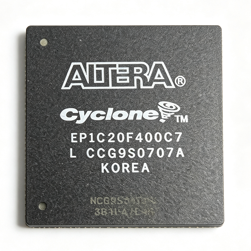
EP1C20F400C7 - Cyclone FPGA 20,060 LE 301 I/O 400-BGA | Intel
The Intel (Altera) EP1C20F400C7 is a member of the original Cyclone family of low-cost Field Programmable Gate Arrays (FPGAs), offering 20,060 logic elements, 294,912 bits of embedded RAM, 301 user I/O pins, and a 400-ball FineLine BGA package operating from a 1.5 V core supply. Built on a 0.13 µm SRAM process, it targets cost-sensitive high-volume applications where ASIC-class integration is unnecessary and time-to-market dominates. An FPGA (Field Programmable Gate Array) is a reprogrammable logic device whose internal architecture consists of configurable logic blocks (CLBs), programmable interconnects, embedded memory blocks, and a perimeter of user I/O cells. In the taxonomy of digital semiconductors, FPGAs sit between ASICs (highest NRE, lowest unit cost at volume) and microcontrollers (fixed hardware, lowest flexibility), making them ideal for glue logic, custom datapaths, and hardware-accelerated DSP. The Cyclone family was Altera's first process-node family explicitly optimized for low power and low unit cost. Key features of the EP1C20F400C7 include 20,060 logic elements arranged in 2,006 logic array blocks (LABs), 288 kbits of embedded SRAM distributed across M4K memory blocks, 301 single-ended I/O (or differential pairs) supporting LVDS, LVTTL, LVCMOS, SSTL, and PCI standards, one PLL per device for clock conditioning, and 20 global clock networks. The 400-ball FineLine BGA package measures 21 mm × 21 mm with a 1.00 mm ball pitch, allowing mid-density PCB designs without via-in-pad or HDI stackups. Technically, the device uses a 4-input look-up table (LUT) as its basic logic element, supports true dual-port and single-port RAM, and provides dedicated multiplier blocks (3 × 3 multipliers) for DSP applications. Configuration is loaded via an industry-standard passive serial (PS), passive parallel synchronous (PPS), passive parallel asynchronous (PPA), or JTAG interface. The Quartus II design software (legacy: 6.0 through 13.1) supports the full design flow from synthesis to programming file generation. Typical applications include industrial control and factory automation, automotive infotainment and driver-assistance subsystems, consumer video processing, communications line cards, and prototyping platforms for ASIC emulation. The combination of high logic density, modest power envelope, and a JTAG-based debug interface also makes the EP1C20F400C7 a popular choice in university curricula for teaching digital design with a real silicon target. When designing with this part, engineers should plan for 1.5 V core decoupling with multiple 0.1 µF + bulk capacitors, observe the LVDS I/O banking rules (each bank has a VCCIO reference), and use the Altera ByteBlaster II or USB-Blaster cable for in-system programming. The 400-BGA package requires careful PCB layout: matched-length traces for clock pairs, and a thermal copper pour under the package to spread the moderate (~1.5 W typical) dissipation. This page synthesizes distributor pricing, drop-in same-density alternatives, and practical design notes not found in the legacy Cyclone datasheet alone.
EP1C20F400C7N - Cyclone FPGA 20K LE 400-FBGA | Altera
The Altera (Intel) EP1C20F400C7N is a Cyclone-series Field-Programmable Gate Array (FPGA) with 20,060 logic elements, 294,912 bits of embedded RAM, and 301 user I/O pins, housed in a 400-ball FineLine BGA package. It is fabricated on a 130 nm CMOS process and operates at a core voltage of 1.5 V, with commercial temperature grade (0 °C to +85 °C) and a -7 speed grade targeting approximately 405 MHz internal operation. An FPGA (Field-Programmable Gate Array) is a type of programmable logic device (PLD) that allows engineers to implement custom digital logic through a sea of configurable logic blocks (CLBs), embedded multipliers, memory blocks, and programmable I/O. Within the broader semiconductor taxonomy, FPGAs sit under programmable logic -> logic ICs -> integrated circuits, and they bridge the gap between ASICs (high NRE, high volume) and discrete logic (low density, fixed function). The Cyclone family was Altera's low-cost, high-volume FPGA line, positioned against Xilinx Spartan-3 and later Spartan-6. Key features of the EP1C20F400C7N include 20,060 logic elements distributed across 2,006 logic array blocks (LABs), 288 Kbits of dedicated RAM organized as M4K memory blocks, up to 52 embedded 18 x 18 multipliers for DSP workloads, four phase-locked loops (PLLs) for clock management, and support for external memory interfaces including DDR SDRAM and QDR SRAM via dedicated DQS pins. Architecturally, the device uses an SRAM-based configuration cell, requiring an external configuration memory (typically EPCS or EPCQ serial flash) that loads the bitstream over an active serial (AS) or JTAG interface. The 400-ball FineLine BGA exposes up to 301 user I/Os (the remainder are power/ground/configuration), supporting multiple I/O standards such as LVTTL, LVCMOS, SSTL, HSTL, and LVDS through eight I/O banks. Typical applications include industrial control and motor drive logic, video processing pipelines, low-cost communications line cards, glue logic replacement on legacy systems, and educational/prototyping platforms. Its combination of DSP blocks and moderate logic density also suits cost-sensitive image preprocessing and software-defined radio front-end controllers. When designing with this part, note that the Cyclone I family is now in end-of-life status; engineers should plan for migration to Cyclone IV or Cyclone V equivalents for new designs. The 1.5 V core and PLL-based clock tree require careful power sequencing and decoupling per Altera's AN 224 application note. This page synthesizes distributor pricing, verified drop-in speed-grade and package alternatives, and practical design notes that go beyond the manufacturer datasheet to help procurement and FPGA engineers evaluate the EP1C20F400C7N for both new designs and legacy board replacements.
EP1C20F400C8 - Cyclone FPGA 20060 LE 400-BGA | Intel
The Intel (formerly Altera) EP1C20F400C8 is a member of the first-generation Cyclone FPGA family, delivering 20,060 logic elements, 294,912 bits of embedded RAM, and 301 user I/O pins in a 400-ball FineLine BGA package (21 × 21 mm, 1.0 mm pitch). Built on a 130 nm CMOS process and operating from a 1.5 V core supply, it targets cost-sensitive, high-volume designs that need programmable logic without the power and price of Stratix-class devices. An FPGA (Field Programmable Gate Array) is a programmable logic device that lets engineers implement arbitrary digital circuits using an array of configurable logic blocks (CLBs), programmable interconnect, dedicated memory blocks, and hardened I/O cells. FPGAs sit in the programmable logic hierarchy between fixed-function ASICs (high NRE, low unit cost at volume) and microcontrollers (software-defined, sequential); they win when parallelism, deterministic latency, or rapid design iteration is required. Cyclone is Intel's low-cost FPGA tier, above MAX CPLDs and below Cyclone II/III/IV/V in density and feature evolution. Key features include 20,060 logic elements organized as 2,006 logic array blocks (LABs), 64 M4K RAM blocks (128 × 36 bits each, totaling 294,912 bits), up to 301 single-ended or differential LVTTL/LVCMOS/pseudo-differential LVDS/LVDS/RSDS user I/Os, embedded 18 × 18 multipliers for DSP, and a phase-locked loop (PLL) per device quadrant for clock management. The device supports configuration via passive serial (PS), active serial (AS), and JTAG modes using Altera/Intel Quartus design software. Architecturally, the EP1C20F400C8 uses an SRAM-based configuration cell, meaning the bitstream must be loaded from an external configuration PROM or flash at every power-up. The 130 nm process, 1.5 V core, and 1.5 V/1.8 V/2.5 V/3.3 V multi-voltage I/O banks give it 275 MHz internal performance on typical designs. Embedded M4K memory blocks can be configured as RAM, ROM, FIFO, or shift registers; the 18 × 18 multipliers deliver up to 250 MHz DSP throughput suitable for video line buffers, motor control, and basic FIR filtering. Typical applications include digital video surveillance, industrial control planes (I/O expansion for PLCs), motor drive interface logic, consumer display controllers, software-defined radio (SDR) baseband pre-processing, and legacy glue logic replacement for systems that have outgrown 74-series or CPLD density. The 301 user I/Os and abundant M4K memory make it a strong fit for image-sensor bridging and bus-protocol bridging (PCI to local bus, async SRAM to DDR, etc.). When designing with this device, prefer 4-layer PCB stack-ups with continuous VCCINT and GND planes to keep core supply noise under 30 mV peak-to-peak; the exposed die paddle (if used) must be soldered for thermal relief. Designers should plan to migrate to Cyclone II (EP2C20) or Cyclone IV (EP4CE22) for new designs, because Cyclone I is mature/NRND and many configuration tools now warn about legacy device support. This page synthesizes distributor pricing, same-family drop-in alternatives, and practical design notes not found on the manufacturer datasheet.
EP1C20F400C8N - Cyclone FPGA, 20K LE, 301 I/O | Intel
The Intel (Altera) EP1C20F400C8N is a Cyclone-series field-programmable gate array (FPGA) with 20,060 logic elements, 294,912 RAM bits, and 301 user I/O pins in a 400-ball FineLine BGA (FBGA-400) package. The ordering code C8N identifies commercial-temperature grade C, speed grade 8, and an N lead-free finish, making the device suitable for RoHS-leaning production boards where an entry-level FPGA with high board-level I/O is required. What is an FPGA? A field-programmable gate array is an integrated circuit whose logic fabric, routing, and I/O behavior can be configured after manufacturing by loading a bitstream. FPGAs sit between fixed-function ASICs and generic processors: they provide parallel, deterministic custom hardware while allowing design changes without mask re-spin. In the silicon hierarchy, FPGAs are complex digital ICs supported by power supplies, clock oscillators, configuration memories, and level translators. The Cyclone family was Altera's low-cost FPGA line, and EP1C20 is one of its mid-capacity devices, intended for cost-sensitive applications that still need parallel I/O processing. The main design assets are its logic and I/O count. The 20,060 logic elements implement combinational and sequential logic with embedded registers, while the 294,912 RAM bits can be used as FIFOs, small buffers, or register files. The 301 user I/O pins across the 400-ball FBGA allow board designers to attach many peripherals directly to the FPGA, reducing glue logic. As a commercial-speed-grade-8 product, it balances price and timing for designs that do not require the fastest speed sorting. From an architectural standpoint, this Cyclone FPGA is SRAM-based, so an external configuration source must reload the bitstream at every power-up. The BGA package permits dense connectivity but requires a multi-layer PCB and proper decoupling. The C8N variant with N finish is intended for lead-free solder processes, aligning with modern assembly houses. Designers should use the manufacturer's pin planning and power estimator tools before layout. Typical uses include industrial control logic, video and image capture front ends, communication protocol bridging, ASIC prototyping, and distributed I/O controllers. For designs that fit inside 20,060 logic elements, this device can replace many fixed-function PLDs or CPLDs while offering a reprogrammable pin assignment and parallel datapath. During board design, budget for an external configuration source and use the FPGA vendor's power and pin planning tools to align I/O bank voltage assignments before layout. Because this is a mature component, use existing reference designs for the configuration interface and verify the exact OPN before purchasing. This page synthesizes verified distributor specifications, drop-in Cyclone-family alternatives, package and grade trade-offs, and practical design guidance not repeated in every supplier listing. It is intended to help engineers make a sourcing decision quickly and accurately for the EP1C20F400C8N.
EP1C20F400C8NAC - 20,060-Cell, 1.5V Cyclone FPGA | Intel | Embedded Logic
Intel EP1C20F400C8NAC is a Cyclone-family field-programmable gate array containing 20,060 logic cells, operating at a listed frequency of 275.03 MHz, and built using 130 nm technology. It uses a 1.5 V supply and is housed in a 400-pin FBGA package. The device provides 301 I/O according to distributor and technical-index listings, making it a high-I/O-density programmable logic option for embedded systems, industrial controls, communications equipment, and legacy digital designs. An FPGA, or field-programmable gate array, is a semiconductor device composed of configurable logic blocks, programmable interconnects, and programmable I/O resources. Unlike a fixed-function application-specific integrated circuit, an FPGA can be configured after manufacturing to implement combinational logic, sequential state machines, interface bridges, and digital signal-processing datapaths. Within the semiconductor hierarchy, EP1C20F400C8NAC belongs to the programmable-logic-device category and specifically the FPGA family. Its configurable architecture allows engineers to adapt hardware behavior without fabricating a new integrated circuit. The principal listed specifications are 20,060 cells, 275.03 MHz, and 130 nm process technology. The device is identified as a 1.5 V FPGA and is offered in a 400-pin FBGA package. The listed 301 I/O count provides substantial external connectivity for parallel buses, control interfaces, and data-acquisition systems. The Cyclone architecture is suited to designs that require programmable glue logic, protocol conversion, timing control, and configurable peripheral integration. EP1C20F400C8NAC is positioned for legacy and established programmable-logic platforms rather than modern high-performance FPGA implementations. The 130 nm process and 1.5 V supply indicate an older device generation, so designers should validate available design software, configuration memory requirements, timing constraints, and long-term lifecycle planning before starting a new production program. The large 400-pin package also requires careful PCB fan-out, controlled-impedance routing, and thorough power-distribution analysis. Typical applications include industrial automation controllers, embedded communications interfaces, test and measurement equipment, image or data-acquisition front ends, motor-control peripherals, and custom interface bridges. Its 301 listed I/O resources are useful where multiple digital buses, sensor interfaces, or control signals must be aggregated. In communications equipment, the FPGA can implement protocol adaptation, framing, error handling, or timing conversion. In industrial systems, it can combine control logic, status monitoring, and legacy bus interfaces in one configurable device. A key design consideration is software and toolchain compatibility. Because EP1C20F400C8NAC is an older Cyclone-family device, engineers should confirm the exact supported Intel or Altera Quartus software generation, device-fit status, configuration interface, and available intellectual-property cores. Verify pin assignments, bank voltages, clocking resources, I/O standards, and package thermal requirements directly from the manufacturer documentation before release to layout or production. This product page combines verified device specifications, package and supply context, sourcing observations, engineering applications, and strict drop-in-alternative screening. It is intended to help buyers and engineers distinguish electrically documented candidates from unverified substitutes while preserving the 400-pin FBGA footprint requirement.
EP1C20F400I-6 - Cyclone FPGA 20,060 LE BGA-400 | Intel / Altera
The Intel (formerly Altera) EP1C20F400I-6 is a member of the first-generation Cyclone FPGA family, delivering 20,060 logic elements in a 400-ball FineLine BGA package with industrial temperature grade (-40C to +85C) and a -6 speed grade. Built on a 1.5V core, 0.13um SRAM process, the device is positioned for cost-sensitive, high-volume designs that need true programmable logic without the power or cost penalty of higher-density FPGAs. A Field-Programmable Gate Array (FPGA) is a semiconductor integrated circuit whose digital logic function is defined by user-loaded configuration memory rather than fixed mask layers, sitting in the broader hierarchy: programmable logic -> logic IC -> integrated circuit -> semiconductor. Cyclone was Altera's first family to explicitly target ASIC replacement in consumer, communications, and industrial DSP, and the EP1C20 sits at the upper end of that first-generation family. Key features of the EP1C20F400I-6 include 20,060 logic elements, 294,912 bits of embedded RAM (M4K blocks), 244 embedded 18x18 multipliers (hard DSP blocks), up to 301 user I/O pins, four phase-locked loops for clock management, and support for LVDS, LVTTL, LVCMOS, SSTL, and PCI I/O standards. The -6 speed grade specifies the slowest of the Cyclone tiers, favoring power and yield over raw Fmax. Architecturally, the EP1C20 uses a four-input look-up table (LUT) fabric with embedded multiplier blocks, dedicated M4K RAM blocks (4 Kbits each, true dual-port capable), and global clock networks routed through the four PLLs. Configuration is loaded from passive serial (PS), active serial (AS), or JTAG, with bitstream encryption available on higher tiers but not on Cyclone. The 400-ball FineLine BGA (1.0 mm pitch) provides ample routing escape for high I/O counts while keeping board complexity manageable. Typical applications include digital signal processing for industrial control, glue logic and bus bridging in telecom line cards, video processing front-ends, low-cost automotive infotainment subsystems, and ASIC prototyping. The embedded 18x18 multipliers are particularly suited to FIR filters and FFT butterfly stages. Industrial-grade temperature range makes the device acceptable for factory automation and outdoor communications gear. When designing with the EP1C20F400I-6, careful attention to power sequencing and decoupling is critical: the 1.5V VCCINT must ramp monotonically before VCCIO to avoid I/O latch-up. Use the Quartus II design software (or its modern equivalent) for synthesis, placement, and timing closure. Note that the Cyclone family is end-of-life; new designs should evaluate Cyclone IV/V or MAX 10 for active production. This page synthesizes distributor stock data, parametric alternatives, and practical design notes that go beyond the original Altera Cyclone family datasheet, helping engineers determine whether to sustain an existing EP1C20 design or migrate to a modern equivalent.
EP1C20F400I6 - Cyclone FPGA, 20060 LEs, 400-FBGA | Altera
The Altera (now Intel) EP1C20F400I6 is a member of the original Cyclone FPGA family fabricated on a 1.5 V, 130 nm SRAM-based process, offering 20,060 logic elements in a 400-ball FineLine BGA package with industrial temperature grading. The device integrates 288 Kbits of embedded RAM organized as M4K blocks, supports up to 301 user I/O pins, and includes two PLL blocks for clock management. Typical core operating frequency reaches 405.2 MHz as listed in third-party parametric summaries. A Field-Programmable Gate Array (FPGA) is a reconfigurable semiconductor device in which the logic fabric, interconnect, and I/O cells can be programmed after manufacture using a hardware description language (HDL) such as Verilog or VHDL. FPGAs sit at the top of the digital logic hierarchy alongside ASICs and CPLDs, sitting above microcontrollers in performance-per-watt for highly parallel workloads. Within the broader taxonomy, the Cyclone family belongs to the low-cost, high-volume FPGA segment optimized for glue logic, bus bridging, and DSP pre-processing rather than the high-end transceiver-rich Stratix tier. Key features include support for LVDS, LVTTL, LVCMOS, SSTL-2, and SSTL-3 I/O standards; embedded multipliers for low-cost DSP; and a serial configuration interface compatible with EPCS serial configuration devices. The device operates from a 1.5 V core supply with separate VCCIO banks for flexible I/O voltage rails, and it supports passive or active serial configuration schemes plus JTAG boundary-scan testing per IEEE 1149.1. The Cyclone architecture uses a 2-D row-and-column interconnect with embedded M4K RAM blocks, LAB (Logic Array Block) clusters of 10 logic elements each, and dedicated multiplier blocks for DSP operations. Industrial-grade silicon rated from -40C to +100C ambient ensures reliable operation in factory automation, automotive test, and outdoor wireless backhaul equipment. Typical applications include industrial control and factory automation bridges, low-cost video processing pipelines, motor control and encoder interfaces, telecommunications line-card glue logic, and consumer electronics requiring parallel DSP pre-processing. The Cyclone family is widely used in education for HDL coursework and in prototype ASIC emulation because of its low non-recurring engineering cost. Designers should plan for separate analog and digital ground returns under the BGA, keep PLL analog supply pins LC-filtered, and reference the Quartus II (or the latest Intel Quartus Prime) device handbook for pin assignments and timing closure. The 400-ball FBGA requires 1.0 mm ball pitch, which dictates PCB stack-up and via-in-pad process selection.
EP1C20F400I7 - Cyclone FPGA 20K LE FBGA-400 | Intel
The Intel EP1C20F400I7 is a member of the first-generation Cyclone FPGA family, delivering 20,060 logic elements and 294,912 bits of embedded RAM in a 400-ball FineLine BGA (FBGA-400) package. Built on a 0.13 µm CMOS process, the Cyclone EP1C20 supports up to 301 user I/O pins with LVTTL, LVCMOS, SSTL, and LVDS I/O standards. The "I7" speed grade combined with the industrial temperature range (-40C to +100C junction) makes this variant suitable for industrial and telecom applications where the C-speed (commercial) parts cannot be used. An FPGA (Field Programmable Gate Array) is a programmable logic device that allows hardware designers to implement custom digital circuits after PCB fabrication. The hierarchy places FPGAs above CPLDs (smaller, non-volatile logic devices) and below ASICs (fixed-function Application-Specific Integrated Circuits) within the broader digital semiconductor category. Cyclone FPGAs target cost-sensitive, high-volume applications by trimming unused silicon (no transceivers, no hardware multipliers in the base Cyclone), keeping die area and unit price low compared to higher-tier Stratix parts. Key features of the EP1C20F400I7 include 20,060 logic elements, 64 embedded 18x18 multipliers (M4K blocks repurposed), a dedicated Double Data Rate (DDR) SDRAM interface supporting up to 133 MHz, and a Phase-Locked Loop (PLL) array for clock synthesis. The device is configured via active serial (AS), passive serial (PS), or JTAG modes using the dedicated configuration pins. The architecture is built around a four-input LUT (Look-Up Table) based logic element fabric with embedded M4K memory blocks (4 Kbit each, total 60 blocks). Distributed RAM and shift-register logic can be inferred from the LUTs themselves, providing flexible on-chip storage. Two PLLs and global clock networks handle clock distribution and frequency synthesis across the die. Typical applications for the EP1C20F400I7 include industrial control boards, video processing front-ends, low-end networking line cards, glue logic replacement, and DSP co-processing. The large logic capacity allows the device to host soft processor cores such as the Nios II, enabling full system-on-chip designs on a single programmable device. When designing with this device, ensure proper decoupling (0.1 µF per power pin plus bulk capacitors), follow Intel's configuration pin recommendations, and select the I7 speed grade carefully — it is the slowest industrial variant, so timing closure on 100 MHz+ designs may require extra pipelining. This page synthesizes distributor pricing, drop-in alternatives, and practical design notes not found in the manufacturer datasheet alone.
EP1C20F400I7N - Cyclone FPGA 20,060 LE 301 I/O 400-BGA | Intel
The Intel (formerly Altera) EP1C20F400I7N is a Cyclone-series Field-Programmable Gate Array (FPGA) featuring 20,060 logic elements, 294,912 bits of embedded RAM, and 301 user I/O pins, housed in a 400-ball FineLine BGA package (21 mm × 21 mm, 1 mm pitch). Built on a 1.5 V core, 0.13 µm SRAM process, the device integrates 2,006 Logic Array Blocks (LABs) and 20 embedded 4-Kbit memory blocks, with PLL-based clock management and dedicated DDR SDRAM interfaces. A Field-Programmable Gate Array (FPGA) is a type of integrated circuit that can be configured by the customer after manufacture using a hardware description language (HDL) such as Verilog or VHDL. FPGAs belong to the broader category of programmable logic devices (PLDs) within the semiconductor hierarchy: programmable logic device → FPGA → SRAM-based FPGA → low-cost FPGA (Cyclone class). They are widely used to implement custom digital logic, glue logic, DSP pipelines, and high-speed interface bridges. Key features of the EP1C20F400I7N include up to 20,060 logic elements, 244,800 typical gates, 294,912 RAM bits organized as M4K memory blocks, and 301 user I/O with support for multiple I/O standards including LVTTL, LVCMOS, SSTL, and LVDS. The device also provides up to two PLLs with four outputs each for clock synthesis and skew management, and dedicated hardware multipliers for low-cost DSP. The Cyclone architecture uses a 2-D row-and-column routing network driven by look-up tables (LUTs) with embedded carry chains for arithmetic. SRAM configuration cells store the user design and are loaded at power-up from external flash or a configuration device, supporting passive serial, active serial, and JTAG modes. Per-pin signal-integrity features such as slew-rate control and drive-strength programming simplify PCB design. Typical applications include industrial control and factory automation glue logic, low-cost video processing, communications protocol bridging (PCI, UART, SPI), and consumer-electronics controllers. The 400-BGA package supports high I/O count designs while maintaining a compact 21×21 mm footprint for moderate-density boards. When designing with the EP1C20F400I7N, ensure the power tree provides a clean 1.5 V core supply with adequate bulk and decoupling, and verify configuration mode selection against your chosen boot source. Industrial-grade (-40 °C to +100 °C junction) variants such as the I7N speed grade are required for environments beyond commercial temperature ranges. This page synthesizes drop-in alternatives, parametric comparisons, and practical design notes beyond the manufacturer datasheet to accelerate schematic entry, BOM selection, and supply-chain qualification.

EP1C3T10017N - 2,910 LEs Cyclone FPGA, TQFP-100 | Intel / Altera
The Intel (formerly Altera) EP1C3T10017N is a low-cost Cyclone FPGA from the first-generation Cyclone family, featuring 2,910 logic elements, 58,848 bits of embedded RAM, and a single global PLL in a 100-pin TQFP package. The "17" speed grade and "N" suffix indicate a commercial-temperature, lead-free, industrial-grade part with typical -7 speed characteristics, supporting clock rates suitable for glue-logic, custom peripheral bridging, and modest DSP pipelines. The Cyclone family is Intel's first SRAM-based, low-cost FPGA architecture, positioned in the broader taxonomy as FPGA -> programmable logic device -> logic IC -> integrated circuit. Cyclone devices were introduced in 2002 to address cost-sensitive ASIC replacement and are typically used where logic density in the 2K-20K LE range is sufficient but a microcontroller lacks flexibility. Cyclone FPGAs are fabricated on a 0.13-micron CMOS process with a 4-input look-up table (LUT) based logic element, embedded M4K RAM blocks, and dedicated I/O structures supporting LVTTL, LVCMOS, PCI, and other common single-ended standards. Key features of the EP1C3T10017N include 2,910 LEs, 13 embedded M4K RAM blocks (58,848 total RAM bits), one PLL providing clock multiplication, division, and phase shifting, and up to 65 user I/O pins across 4 I/O banks. The device supports configuration via passive serial (PS), active serial (AS) with an Altera configuration device, or JTAG. The TQFP-100 (1.0 mm pitch, 14x14 mm body) package enables low-cost PCB assembly on standard FR-4 substrates without the need for advanced HDI stack-ups. The Cyclone LE architecture combines a 4-input LUT with a configurable register, allowing each LE to implement either combinational logic or a flip-flop. Embedded multiplier blocks (in larger Cyclone variants) and the distributed M4K memory blocks provide on-chip storage for FIFO buffers, look-up tables, and small data caches. The single PLL block supports output frequencies up to several hundred MHz and can deskew external clocks, generate multiple phase-related domains, or compensate for board-level skew. Typical applications for the EP1C3T10017N include consumer-electronics glue logic, custom interface bridging (I2C/SPI/UART expansion, LCD/LED display controllers), industrial control and sensor aggregation, low-cost prototyping for ASIC replacement, education kits, and legacy system maintenance. Designers often select the EP1C3 for its combination of small footprint, low unit cost, and compatibility with the mature Quartus II design toolchain. When designing with the EP1C3T10017N, pay careful attention to I/O bank voltage compatibility - the device supports separate VREF and VCCIO rails per bank, but mixing 3.3V and 5V TTL inputs on the same bank without proper VCCIO selection can cause long-term reliability issues. Use Quartus II 13.0sp1 or earlier for legacy support, or migrate to a Cyclone IV or Cyclone 10 LP device for new designs. This page consolidates distributor pricing, drop-in same-family alternatives, and practical design notes that go beyond the manufacturer datasheet, helping procurement and FPGA engineers evaluate the EP1C3T10017N for both new and legacy designs.
EP1C3T100C6 - Cyclone FPGA 2910 LE 100-TQFP | Intel / Altera
The Intel / Altera EP1C3T100C6 is a Cyclone-family low-cost Field-Programmable Gate Array (FPGA) containing 2,910 logic elements across 65 LABs (Logic Array Blocks), packaged in a 100-pin TQFP (Thin Quad Flat Pack) and fabricated on a 130 nm CMOS process that operates from a 1.5 V core supply. It is one of the smallest members of the original Cyclone (Cyclone I) family, designed for high-volume, cost-sensitive digital logic applications such as glue logic, I/O expansion, bridging, and simple state-machine control. According to the Altera Cyclone Device Family datasheet (94 pages), the EP1C3T100C6 features a maximum internal operating frequency around 405.2 MHz, up to 59,904 RAM bits of embedded memory, and a single PLL with up to three output clocks for flexible clock management. A Field-Programmable Gate Array (FPGA) is a programmable logic device containing an array of configurable logic blocks (CLBs), programmable interconnect, and I/O cells, all of which can be reconfigured by the user after manufacture. Within the broader semiconductor taxonomy, an FPGA sits between a general-purpose microcontroller and a fixed-function ASIC: faster and more parallel than a microcontroller for parallel data-path tasks, yet cheaper and more flexible than an ASIC at low-to-medium volumes. The Cyclone I family was Altera's first low-cost FPGA line and is hierarchical under: FPGA -> programmable logic device -> logic IC -> integrated circuit -> semiconductor. Key features of the EP1C3T100C6 include 65 user I/O pins on the TQFP-100 package, 1.5 V core voltage with 3.3 V I/O tolerance, 130 nm process technology, JTAG-based in-system programming via the Altera ByteBlaster or USB-Blaster, support for LVTTL, LVCMOS, SSTL-2, and SSTL-3 I/O standards, and an operating junction temperature of 0 C to +85 C (commercial grade, indicated by the C6 speed-grade suffix meaning -6 speed grade, commercial temperature range). The exposed thermal pad on the bottom of the TQFP package helps dissipate the modest power dissipation typical of this small device. From an architectural perspective, the Cyclone I device uses 4-input look-up tables (4-LUTs) as its basic logic element, embedded M4K memory blocks of 4 Kbits each (delivering 13 M4K blocks / ~52 Kbits usable per block family-wide), and a unified interconnect fabric called MultiTrack that minimizes routing congestion. The single PLL provides clock multiplication, division, and phase shifting, which is sufficient for most glue-logic and protocol-bridge designs but limits the device compared to larger Cyclone variants with multiple PLLs. Typical applications include digital I/O expansion for microcontrollers, custom peripheral bridging (UART, SPI, I2C, or parallel bus glue logic), simple video or display timing controllers, low-cost industrial control boards, educational FPGA development platforms, and prototype ASIC replacement for designs later migrating to a structured ASIC or Cyclone II/III/IV. The combination of 100-pin TQFP (hand-solderable and breadboard-friendly via adapter) and Quartus II Web Edition software support makes it a popular choice in academic and maker communities. When designing with the EP1C3T100C6, observe the 1.5 V VCCINT supply and 3.3 V VCCIO I/O supply requirement with proper decoupling (100 nF and 10 uF bulk near each supply pin). Programming via JTAG requires a 10-pin header wired per the Altera ByteBlaster II / USB-Blaster pinout. Unused I/O pins should be left floating or configured as outputs driving low to minimize switching current. This page synthesizes distributor pricing, drop-in pin-compatible Cyclone I alternatives, and practical Quartus II design notes not collected in any single manufacturer document.
EP1C3T100C6N - Cyclone FPGA, 2,910 LEs, 100-TQFP | Altera
The Altera (Intel Programmable Solutions Group) EP1C3T100C6N is a low-cost Cyclone FPGA with 2,910 logic elements, 59,904 RAM bits, and 65 user I/O pins housed in a 100-pin TQFP package. Built on a 0.13 µm SRAM process, it operates from a 1.5 V core supply with separate VCCIO banks supporting multiple I/O standards including LVTTL, LVCMOS, PCI, and LVDS. A Field Programmable Gate Array (FPGA) is a semiconductor device built around an array of configurable logic blocks (CLBs), programmable interconnects, and I/O cells that can be re-programmed after manufacture to implement arbitrary digital logic. Within the broader taxonomy, an FPGA sits at the intersection of programmable logic devices (PLDs) and application-specific integrated circuits (ASICs), offering hardware-level parallelism, reconfigurability, and faster time-to-market than ASICs while delivering higher logic density than CPLDs. Cyclone family parts specifically target cost-sensitive, high-volume applications where ASIC NRE costs cannot be justified. Key features of the EP1C3T100C6N include 13 embedded 18x18 multipliers suited for DSP functions such as FIR filters and FFTs, one PLL providing clock multiplication, phase shifting, and duty-cycle control, and on-chip configuration memory with active serial (AS), passive serial (PS), and JTAG programming modes. The device supports up to 20 global clock networks and hardware multipliers that are essential for digital signal processing pipelines. The Cyclone architecture uses 4-input look-up tables (LUTs) as the fundamental logic element, paired with embedded M4K RAM blocks that can be configured as single-port, dual-port, or FIFO memory. Each M4K block provides 4,608 bits with parity support. The device interfaces with external configuration devices such as the EPCS1/EPCS4 serial flash for active serial configuration, supporting in-system programmability through JTAG. Typical applications include consumer video processing, industrial control logic, automotive infotainment prototypes, low-cost PCI bridging, and educational development platforms. The 100-TQFP package and commercial temperature grade make it especially suitable for prototype boards, evaluation kits, and university labs where through-hole-friendly footprints simplify bring-up. When designing with this part, pay close attention to I/O bank voltage compatibility, as mixing LVTTL and LVCMOS standards requires careful VCCIO assignment per bank. Decoupling requires at least 0.1 µF capacitors near every VCC pin plus bulk capacitors on each supply rail. Unused pins should be configured as inputs with weak pull-ups to reduce inrush current during configuration. This page synthesizes distributor pricing, drop-in Cyclone and competitor alternatives, and practical design notes not found in the manufacturer datasheet, with data verified against the latest web sources as of 2026-09-06.
EP1C3T100C7 - Cyclone 2910 LEs FPGA, 65 I/O, 100-TQFP | Intel
The Intel (formerly Altera) EP1C3T100C7 is a low-cost Cyclone FPGA from the original Cyclone family, delivering 2,910 logic elements and 59,904 RAM bits in a 100-pin TQFP (TQFP-100) package. Manufactured on a 130 nm process and built around a 1.5 V core supply, this Cyclone-I device targets high-volume, cost-sensitive glue-logic and control-plane applications where ASSPs and CPLDs run out of headroom. An FPGA (Field Programmable Gate Array) is a programmable logic device consisting of an array of configurable logic blocks (CLBs), programmable interconnect, and I/O cells, all controlled by a user-defined bitstream. FPGAs sit in the programmable logic hierarchy between simple PLDs/CPLDs (limited gates, fixed architecture) and ASICs (custom silicon, high NRE). Cyclone sits at the low-cost end of the FPGA family tree: SRAM-based look-up tables backed by embedded RAM blocks and PLL-based clock management. Because the bitstream is loaded from an external configuration flash, the same silicon can be re-used across product revisions - a key advantage over fixed-function ASICs. Key Cyclone features include 2,910 LEs, 13 embedded M4K RAM blocks (59,904 total RAM bits, 4 Kbits each), one PLL, and 65 user I/O pins brought out on the 100-TQFP. The device supports LVTTL, LVCMOS, SSTL, and LVDS I/O standards and exposes up to 320.1 MHz internal performance. Configuration is via Altera passive serial (AS), active serial, or JTAG. The part is specified over the commercial 0C to +85C junction range with the C7 speed grade. The Cyclone-I architecture uses 4-input LUTs for combinational logic, dedicated carry chains for fast adders, and LABs (Logic Array Blocks) grouping 10 LEs for efficient routing. Embedded M4K blocks double as true dual-port RAM, simple dual-port RAM, or ROM, enabling FIFOs, lookup tables, and small cache/line buffers inside the fabric. Typical applications include industrial control and machine I/O glue, motor-control co-processors, video format conversion bridges, low-cost display controllers, and replacement of multiple 74-series TTL packages on legacy boards. The 100-TQFP footprint is friendly for hand-prototyping and low-speed signal access on two-layer boards. When designing with Cyclone-I, observe the 1.5 V core rail sequencing (VCCINT must precede or track VCCIO within datasheet limits) and reserve a JTAG header for in-system programming. For new designs today, prefer Cyclone-IV or Cyclone-V, but the EP1C3T100C7 remains in service for long-lifecycle industrial and medical equipment.