Interface ICs
ژێرپۆلەکان
بەرهەمەکان (560+)

P82B96DP,118 - Dual I2C Bus Buffer 400kHz TSSOP-8 | NXP
The NXP Semiconductors P82B96DP,118 is a dual bidirectional bus buffer that creates a non-latching, bidirectional logic interface between the normal I2C-bus and a range of other bus configurations, supporting data rates up to 400 kHz, bus voltage levels from 2 V to 15 V, in an 8-pin TSSOP (DP) package. A bidirectional bus buffer, also called an I2C buffer or bus extender, sits between an I2C or SMBus controller and its remote peripherals to isolate capacitance, extend cable reach, and translate voltage levels. Within the interface IC hierarchy (bus buffer -> interface IC -> communication IC -> semiconductor), buffers like the P82B96 are essential whenever total bus capacitance exceeds the standard 400 pF limit of the I2C-bus specification (UM10204). Key features include two independent buffer channels, non-latching bidirectional signal transfer that preserves the wired-AND I2C arbitration scheme, and support for buffer outputs at higher voltage and current levels than standard I2C logic. Because the device is bipolar, its Tx/Rx and Ty/Ry pins use standard I2C logic levels while the Sx/Sy side can drive buses at different voltage and current levels, including long cables. Technically, the P82B96 splits each bidirectional line into an input (Tx/Ty), an open-drain buffer output (Rx/Ry), and a Schmitt-type connection (Sx/Sy) that can interface to other bus configurations or a second P82B96 for cascaded level translation. This architecture enables 40 m cable lengths at 400 kHz per NXP product data, far beyond native I2C limits. Typical applications include I2C bus extension over cables in industrial automation and process control, level translation between 3.3 V, 5 V and 12-15 V bus segments, and splitting a single master bus into isolated zones in sensing and instrumentation systems. A key design consideration: each buffer stage adds a small propagation delay and output low voltage offset, so pull-up resistor values on the buffered side should be recalculated to maintain noise margins. This page synthesizes distributor pricing, drop-in alternatives, and practical design notes not found in the manufacturer datasheet.

P82B96TD - Dual I2C Bus Buffer 2-15V 400kHz | NXP
The NXP Semiconductors P82B96TD is a dual bidirectional I2C bus buffer that creates a non-latching, bidirectional logic interface between a standard I2C-bus and bus configurations with different voltage and current levels, operating from 2 V to 15 V at up to 400 kHz in an 8-pin SOIC (SO8) package. An I2C bus buffer, also called a bus repeater or redriver, is an interface IC that sits between an I2C master and one or more slaves to isolate bus capacitance, translate logic levels, and extend cable length. Within the signal-integrity hierarchy (bus buffer -> line driver -> interface IC -> signal conditioning IC), buffers like the P82B96TD allow a small I2C segment to drive long or heavily loaded lines without violating the 400 pF bus capacitance limit of the standard I2C specification. Key features include two independent buffer channels handling both SCL and SDA, a wide supply range of 2 V to 15 V, support for 15 V bus levels and low-impedance lines, and low operating supply current of approximately 900 uA. The bipolar process is latch-up free and provides ESD protection exceeding 3500 V HBM per JESD22-A114, 250 V MM (DIP package) per JESD22-A115, and 1000 V CDM per JESD22-C101. The buffer splits each I2C signal into forward and reverse paths (Tx/Rx and Ty/Ry), using slightly different logic-low voltage levels at the Sx/Sy side to prevent latch-up without a direction-control pin. This architecture allows interfacing between standard 3.3 V or 5 V I2C logic, the 350 uA SMBus, and 15 V level systems on the same PCB. Typical applications include I2C bus extension over long cables, level shifting between 3.3 V microcontrollers and 5 V or 15 V peripherals, capacitive bus isolation for large multi-drop networks, and SMBus-to-I2C interfacing in industrial and telecom systems. Design consideration: two or more Sx or Sy pins must never be connected to the same node, as the architecture does not support this; when cascading buffers, connect Tx/Rx signals of one stage to Sx/Sy of the next. Pull-up resistor sizing must account for the offset logic-low levels at Sx/Sy. This page synthesizes distributor availability data, verified drop-in alternatives, and practical design notes not found in the manufacturer datasheet.
P82B96TD,112 - Dual I2C Bus Buffer 2-15V | NXP
The NXP P82B96TD,112 is a dual bidirectional bus buffer IC that creates a non-latching, bidirectional logic interface between the normal I2C-bus and a range of other bus configurations, housed in an 8-pin SOIC (SO8) package with a supply voltage range of 2 V to 15 V and bus speed support up to 400 kHz. A bus buffer is an interface IC that sits between an I2C-bus master or slave and the physical bus wiring, isolating bus capacitance and translating logic levels. In the power management and interface hierarchy, the P82B96 belongs to the I2C buffer and repeater family, a subset of interface ICs used to extend the length, loading, and voltage tolerance of two-wire serial buses while preserving open-drain bus semantics. Key features include interface capability between standard I2C-bus logic and buses operating at different voltage levels (for example the 350 uA SMBus, 3.3 V logic devices, and 15 V levels), low-impedance line driving for cable extension, and latch-up-free bipolar construction. ESD protection exceeds 3500 V HBM per JESD22-A114, 250 V MM (DIP package) and 400 V MM (SO package) per JESD22-A115, and 1000 V CDM per JESD22-C101. Technically, each buffer channel provides two separate signal paths: a Tx path driving the buffered bus from the I2C side and an Rx path sensing the buffered bus and pulling the I2C pin low. Because Tx and Rx are separate directional signals, they may be connected directly without causing bus latching, or used with optocouplers for galvanic isolation or with balanced twisted-pair transmission lines. Typical applications include extending I2C-bus reach across long cables, level-shifting between 3.3 V and 15 V bus domains, driving heavily loaded backplane buses, and isolating large-capacitance LED display clusters from a microcontroller I2C port. Design consideration: keep pull-up resistor values appropriate to each bus domain; the buffer does not create its own pull-up current, so each bus segment must be terminated to its own logic level. This page synthesizes distributor pricing, drop-in alternatives, comparison tables, and practical design notes not found in the manufacturer datasheet.
P82B96TD/S410,118 - Dual I2C Bus Buffer 400kHz | NXP
The NXP Semiconductors P82B96TD/S410,118 is a dual bidirectional bus buffer IC that creates a non-latching, bidirectional logic interface between the standard I2C-bus and a wide range of other bus configurations, housed in an 8-pin SOIC (SOT96-1) surface-mount package. It operates at data rates up to 400 kHz, supports bus voltage levels from 3 V up to 15 V, and enables reliable I2C communication over bus lines up to 40 m in length. A bus buffer (also called an I2C repeater, level shifter, or bus extender) is an interface IC that isolates and strengthens signal lines in a serial communication system. In the hierarchy of I2C system components, it sits between the I2C master/slave devices and the physical bus, solving problems such as bus capacitance limits, mixed-voltage domains, and long cable runs that a plain two-wire I2C-bus cannot tolerate. The P82B96 belongs to the broader family of interface ICs - signal buffers, repeaters, and redrivers. Key features of the P82B96 include two independent buffer channels that handle both SCL and SDA I2C signals, bidirectional data transfer without latching, and a unique split of each I2C signal into forward and reverse (Tx/Ty and Rx/Ry) signal paths. According to NXP product information, it can interface I2C-bus logic signals to 350 uA SMBus systems, to 3.3 V logic devices, and to 15 V levels and/or low-impedance lines. The bipolar (bipolar transistor) process technology gives it robust drive strength and wide supply tolerance compared with typical CMOS buffers. Technically, each channel presents three ports: a logic-level side for standard I2C systems, and two additional ports that allow level translation between different voltage domains and drive of low-impedance or heavily loaded lines. Because the device is non-latching, it does not suffer from the lock-up issues common to some I2C repeater designs during arbitration or clock stretching. Typical applications include I2C bus extension over long cables (up to 40 m), mixed-voltage interfacing between 3.3 V and 15 V bus segments, SMBus systems, and driving multiple heavily loaded I2C branches in industrial and automotive bodies-electronics environments. A key design consideration: because the buffer passes drive current, the pull-up resistor values on each bus segment must be calculated independently for each side of the buffer rather than for the whole bus. This page synthesizes distributor pricing, drop-in alternatives, pinout data, and practical design notes not found in the manufacturer datasheet.
P82B96TD/S900,118 - 400kHz Dual I2C Bus Buffer SOIC-8 | NXP
The NXP Semiconductors P82B96TD/S900,118 is a dual bidirectional I2C-bus buffer with 400 kHz operation, a 2 V to 15 V supply range, and a 900 uA supply current, housed in an 8-pin SOIC (SOT96-1, 3.90 mm body) package. As a bipolar IC, it creates a non-latching, bidirectional logic interface between the standard I2C-bus and a wide range of other bus configurations, including 3.3 V logic devices, 350 uA SMBus systems, and 15 V or low-impedance bus lines. An I2C bus buffer, also called a bus repeater or redriver, is an interface IC that sits between an I2C master and the bus load. Within the interface IC hierarchy (bus buffer -> signal buffer/repeater -> interface IC -> semiconductor), it solves the classic I2C scaling problems: total bus capacitance limits, cable length, and mixed-voltage interconnection. By splitting SCL and SDA into independent forward (Tx/Ty) and reverse (Rx/Ry) signal pairs, the P82B96 electrically isolates two bus segments while remaining fully non-latching, so lock-up conditions common in simpler repeaters are avoided. Key features include two independent buffer channels handling both SCL and SDA, bidirectional data transfer with a low 5.0 ns propagation delay, and a wide 2 V to 15 V operating supply that lets one side run at 3.3 V or 5 V I2C logic while the other side drives higher-voltage 9 V or 12 V bus lines. Input capacitance is only 7 pF, minimizing loading on the logic-side bus, and supply current is a low 900 uA. Architecturally, the bipolar process gives the P82B96 robust drive strength and high static noise immunity. The Ty/Ry pins can sink up to 30 mA equivalent bus current on the cable side, enabling long cables and heavily loaded backplanes that a standard open-drain I2C port cannot drive directly. Voltage levels on the Sx/Sy side follow normal I2C-bus logic, independent of VCC. Typical applications include mixed-voltage I2C level shifting (3.3 V to 12 V), driving I2C over long cables in industrial control, extending SMBus in servers, and isolating bus segments in telecom and consumer boards. Design tip: connect Tx and Rx pins together when a simple two-way repeater is needed, and keep pull-up resistor values matched to the 400 kHz timing budget. This page synthesizes distributor pricing, drop-in alternatives, and practical design notes not found in the manufacturer datasheet.

PC16550D - UART with 16-Byte FIFOs | Texas Instruments
The Texas Instruments PC16550D is a Universal Asynchronous Receiver/Transmitter (UART) with integrated 16-byte transmit and receive FIFOs, housed in a 40-pin DIP package (offered as PC16550DN from TI). It operates as a single-channel serial-to-parallel and parallel-to-serial converter for CPU-based systems, with the FIFO buffers relieving the processor of per-character interrupt overhead. A UART (Universal Asynchronous Receiver/Transmitter) is a serial communication IC that converts parallel data from a processor bus into asynchronous serial data streams, and back. It sits within the broader hierarchy of interface ICs under the serial communication device class, alongside synchronous counterparts such as USARTs and SPI interfaces. UARTs handle framing, start/stop bit generation, parity checking, and baud-rate generation without a shared clock between endpoints. The PC16550D is an improved version of the original 16450 UART. On power-up it is functionally identical to the 16450 in CHARACTER mode, and it can also be reset to 16450-mode behavior under software control, ensuring backward compatibility with legacy PC and embedded BIOS software. Entering FIFO mode enables the 16-byte buffers on both the transmit and receive paths, dramatically reducing CPU interrupt load compared with the 16450's single-character holding registers. Technical depth: the device includes a programmable baud-rate generator, a modem-control block (DTR, DSR, RTS, CTS, DCD, RI), full line-status reporting, and independently controllable transmit and receive FIFO triggers via its FIFO Control Register (FCR). The RXRDY and TXRDY DMA-handshake signals allow direct memory access transfers, further offloading the host processor in high-throughput serial links. Typical applications include legacy ISA/PCI-era PC COM ports, industrial automation equipment with RS-232/RS-485 links, terminal servers and console-management systems, and embedded processors that need an external memory-mapped UART with modem control. Design consideration: because PC16550D and PC16552D are discontinued by TI, new designs should evaluate the pin/function-compatible TL16C550 family, which TI explicitly discusses as a replacement path in its support forums; verify FIFO trigger behavior and maximum baud rate against the target application. This page synthesizes distributor availability data, the TI/National Semiconductor datasheet, and drop-in replacement analysis not found in the manufacturer datasheet alone.
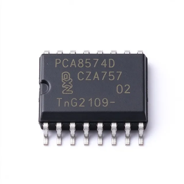
PCA8574D - 8-Bit I2C I/O Expander 400kHz SO16 | NXP
The NXP Semiconductors PCA8574D is a remote 8-bit I/O expander for the I2C-bus with interrupt output, housed in a 16-pin SO16 (SOIC) package. It operates from a 2.3 V to 5.5 V supply, supports a 400 kHz fast-mode I2C interface, and provides eight quasi-bidirectional GPIO ports with three hardware address pins (A0-A2) allowing up to eight devices on one bus. An I/O expander is a peripheral IC that increases the number of general-purpose input/output pins available to a microcontroller over a serial bus. In the power-management and interface hierarchy, the PCA8574D sits between the host MCU and external loads or switches: it belongs to the I2C GPIO expander family, which itself is part of the broader interface IC and remote peripheral category. Expanders save PCB traces, connector pins, and MCU pin budgets in pin-constrained designs. Key features include quasi-bidirectional I/O ports that can be independently assigned as inputs or outputs without a direction register, a latched interrupt output (INT) that flags any input change, totem-pole output capability via the open-drain INT pin, and direct LED driving with 25 mA sink capability per the datasheet family description. The three hardware address pins allow eight PCA8574 devices, or eight each of PCA8574 and PCA8574A, on the same I2C bus - up to 128 I/Os total. Architecturally, the PCA8574D uses a simple register-less command structure: the last written byte defines the port state, and a read returns port pin levels. Power-on reset initializes all ports high (quasi-bidirectional input mode), enabling simple push-button and key-matrix reads without software initialization. Typical applications include keypads and push-button interfaces, LED and backplane status indication, LCD bias and control lines in instrumentation, system monitoring for chassis and rack cards, and spare-I/O expansion in industrial controllers. Design tip: because quasi-bidirectional outputs source only a weak current (100 uA class), drive LEDs and relays by sinking current, and add pull-ups where input levels must be defined. Note: NXP lists the PCA8574D as End of Life. This page adds drop-in replacements, pricing tiers, and design notes beyond the manufacturer datasheet.

PCA8574D,518 - 8-Bit I2C I/O Expander 400kHz SO16 | NXP
The NXP PCA8574D,518 is a remote 8-bit I/O expander for the I2C-bus with interrupt output, operating from 2.3 V to 5.5 V at 400 kHz, housed in a 16-pin SOIC (SO16, 7.50 mm width) package. It provides eight quasi-bidirectional GPIOs, three hardware address pins (A0-A2) allowing eight devices on one bus, and an open-drain active-low interrupt output. An I2C I/O expander is an interface IC that lets a microcontroller add general-purpose input/output lines through the two-wire bidirectional serial bus (SCL, SDA). Within the system hierarchy, it sits in the interface-IC family between the MCU and peripheral loads such as LEDs, buttons, relays and sensors, offloading pin-count-limited controllers without adding parallel-bus complexity. Key features include quasi-bidirectional I/O that can be independently assigned as input or output without direction-control registers, a 400 kHz fast-mode I2C interface, and a latched interrupt output that alerts the host to any input change. The wide 2.3 V to 5.5 V supply range lets one part serve 2.5 V, 3.3 V and 5 V designs. Architecturally, the PCA8574D uses a pseudo-bidirectional port cell: writing a 1 to a bit lets it act as a high-impedance input; writing 0 drives a strong low with controlled sink current. The slave address is 0100 A2 A1 A0 (PCA8574 variant), and the PCA8574A sibling uses 0111, enabling up to 16 expanders (128 I/Os) on one bus. Typical applications include keypad scanning, LED and backlight control, push-button monitoring, relay driving in industrial panels, and sensor-board GPIO expansion where MCU pins are scarce. The interrupt output enables low-power polled designs instead of continuous bus polling. Design consideration: quasi-bidirectional outputs source limited current, so LED loads need the current-sinking wiring convention, and total package sink current must be respected per the datasheet. This page synthesizes distributor pricing, drop-in alternatives, pinout data, and practical design notes not found in the manufacturer datasheet.
PCA9306DCTR - Dual Bidirectional I2C Level Translator | TI
The Texas Instruments PCA9306DCTR is a dual bidirectional I2C-bus and SMBus voltage-level translator with an enable (EN) input, operational from 1.2V to 3.3V on VREF1 and 1.8V to 5.5V on VREF2, housed in an 8-pin SOIC (SM8) package. A voltage-level translator is an interface IC that connects two digital circuits operating at different supply voltages, such as a 1.8V microcontroller driving a 3.3V or 5V sensor bus. Within the interface-IC hierarchy (level translator -> bus switch -> interface IC -> mixed-signal semiconductor), the PCA9306 is a passive-switch architecture: it uses two N-channel pass transistors rather than active driven buffers, so it does not require a direction pin. Key features include bidirectional voltage translation between 1.2V and 5V rails with no direction-control signal, a low ON-state resistance (RON) pass-switch design that minimizes propagation delay and signal distortion, an active-high EN input that isolates both buses when low, and support for I2C, SMBus, PMBus, MDIO, UART, low-speed SDIO, and general two-signal GPIO interfaces. The dual-channel topology handles SCL/SDA or TX/RX pairs in a single package. Architecturally, the PCA9306 uses a gate-drive scheme derived from VREF2 to bias the pass transistors, so the low-side rail (VREF1, 1.2V to 3.3V) is translated up to the high-side rail (VREF2, 1.8V to 5.5V). Because the device is a switch rather than a driver, the open-drain I2C pull-up resistors on each side set the logic levels, preserving multi-master arbitration and clock stretching behavior. Operating temperature range is -40C to +85C. Typical applications include servers, routers and telecom switching equipment, personal computers, and industrial automation systems where a 1.8V/2.5V/3.3V MCU must communicate with 3.3V/5V I2C peripherals such as EEPROMs, sensors, and PMBus power supplies. Design consideration: because RON of the pass switch appears in series with the bus, size the pull-up resistors to account for the added voltage drop at low-side logic-high levels; typical RON values are a few ohms, which is negligible for standard 100kbit/s to 400kbit/s I2C but should be verified for heavily loaded buses. This page synthesizes distributor pricing data, verified drop-in alternatives, pinout details, and practical design notes not found in the manufacturer datasheet, giving engineers a single decision-ready reference.
PCA9507 - I2C Bus Extender 3.3V-5V Level Shift | NXP
The NXP Semiconductors PCA9507 is a 2-wire serial bus extender with integrated 3.3 V to 5 V level shift, supporting bus extension up to 18 meters for reliable HDMI DDC, I2C-bus, and SMBus applications. It is supplied in an 8-pin SOIC (SO) package and buffers one channel at data rates up to 400 kHz. A bus extender, also called an I2C buffer or bus repeater, is an interface IC that sits between a controller segment and a peripheral segment of a two-wire bus. Within the power-management-of-signals hierarchy (bus extender -> I2C buffer/repeater -> interface IC -> semiconductor), its role is to isolate bus capacitance and translate logic levels so that each segment can be optimized independently for drive strength and voltage. Key features include bidirectional buffering of both SDA and SCL, allowing total bus capacitance to exceed the standard 400 pF single-segment limit by splitting it across segments. The built-in level shift permits a 3.3 V controller to talk directly to a 5 V device rail without discrete MOSFET translators. Support for 18 m of cable is roughly 40x the typical practical I2C length, enabled by the accelerator (active pull-up) circuitry that sharpens rising edges. Architecturally, the PCA9507 uses a rise-time accelerator on both sides that sources current into the bus during low-to-high transitions, compensating for RC delay on long cables or heavy loads. This keeps duty cycle distortion low at the 400 kHz Fast-mode ceiling. Because it retains all I2C-bus operating modes during level shifts, multi-master and clock-stretching behavior is preserved. Typical applications include HDMI DDC channel extension between source and display, long-reach SMBus backplanes in servers and telecom racks, and I2C fan-out in industrial control cabinets where sensors sit meters from the master. Design consideration: allocate adequate pull-up resistance per segment - the accelerator assists edges but does not replace pull-ups; verify segment capacitance budget separately on each side of the buffer. This page synthesizes distributor pricing, drop-in alternatives, design notes, and application guidance not found in a single manufacturer datasheet.
PCA9508D,118 - Hot-Swap I2C Level Translating Repeater | NXP
The NXP PCA9508D,118 is a hot-swappable, level-translating I2C-bus repeater housed in an 8-pin SOIC (SO-8, SOT96-1) package, providing bidirectional level shifting between a low-voltage I2C side (down to 0.9 V) and a higher-voltage side (2.7 V to 5.5 V) at bus speeds up to 400 kHz for I2C-bus and SMBus applications. An I2C-bus repeater or bus buffer is an interface IC inserted into an I2C or SMBus segment to extend bus capacitance beyond the standard 400 pF limit, isolate bus segments, and translate between different logic voltage domains. In the power management hierarchy, it sits between the bus controller and peripherals as a signal-conditioning element, distinct from GPIO expanders or I2C switches, because it neither generates addresses nor gates channels - it simply repeats and strengthens bus signals. The PCA9508's headline feature is hot-swap support: the A-side drivers are disabled until the bus is idle and VCC(A) exceeds 0.8 V and VCC(B) exceeds 2.5 V, allowing boards to be inserted into or removed from a live backplane without corrupting bus transactions. Its zero static voltage offset preserves the I2C logic levels, unlike offset-based buffers, so full multi-master arbitration and clock stretching behave transparently across the repeater. Internally the CMOS device uses open-drain driver stages on both sides with rise-time acceleration to drive larger bus capacitance, retaining all I2C operating modes including standard-mode 100 kHz and fast-mode 400 kHz. The EN pin permits system-controlled enable and disable, and should only be toggled when the bus is idle, per the NXP datasheet. Typical applications include live-insertion server and telecom backplanes, mixed-voltage I2C systems bridging 1.2 V or 1.8 V controllers to 3.3 V or 5 V peripherals, and long or heavily loaded bus segments that need capacitive-drive boost. Design consideration: keep EN transitions to idle periods only, and provide pull-up resistors sized to each segment's capacitance, since the repeater does not replace segment pull-ups. This page adds distributor-style alternatives, cross-reference analysis, and design notes beyond what the NXP datasheet alone provides.
PCA9509DP,118 - I2C/SMBus Level Translating Repeater | NXP
The NXP Semiconductors PCA9509DP,118 is a dual-supply level translating I2C-bus/SMBus repeater that buffers both the SDA and SCL lines at up to 400 kHz, housed in an 8-pin TSSOP surface-mount package. It enables a processor-side low-voltage 2-wire serial bus to interface with standard I2C-bus or SMBus I/O while retaining all operating modes of the I2C-bus system during level translation. A level translating I2C buffer (also called an I2C repeater, bus buffer, or redriver) sits between two segments of an I2C or SMBus network. Its role in the signal-chain hierarchy is: bus buffer -> interface IC -> 2-wire serial interconnect. By isolating the two bus segments, it breaks the total bus capacitance into two independent segments, allowing longer trace lengths and more devices per bus than the raw I2C capacitance limit would otherwise permit, while simultaneously shifting logic levels between a lower core voltage domain and a higher peripheral voltage domain. Key features include bidirectional buffering of both SDA and SCL, dual supply pins supporting different voltage domains on each side, and support of the 400 kHz Fast-mode I2C timing class per DigiKey's product listing. Because the device actively drives both segments, rise and fall times are restored on each side, improving signal integrity in capacitive, fan-out-heavy systems. Technically, the repeater uses a rising-edge detector and output driver scheme on each channel so that a LOW on either segment is propagated as a LOW on the other, while allowing either side to pull LOW independently, preserving the wired-AND arbitration and clock-stretching behavior required by the I2C protocol. This makes it transparent to masters and slaves without software configuration. Typical applications include processor low-voltage I2C ports interfacing with standard 3.3V or 5V SMBus peripherals, telecom and server management buses (PMBus/SMBus), and extension of I2C reach in industrial control backplanes. The 8-TSSOP footprint suits dense board layouts where many bus segments must be buffered. Design consideration: keep pull-up resistor values on each segment sized independently for that segment's capacitance and supply, and respect supply sequencing guidance from the manufacturer datasheet for the VCC1/VCC2 domains. This page synthesizes distributor listings, pricing context, and sourcing information for the PCA9509DP,118 in one place, beyond the raw manufacturer datasheet content.

PCA9509GM,125 - I2C/SMBus Level Translating Repeater | NXP
The NXP PCA9509GM,125 is a dual-supply level translating I2C-bus/SMBus repeater in an 8-pin XQFN (SOT902-1, 1.6 x 1.6 mm) package, supporting bus speeds up to 400 kHz and operating from -40C to +85C. An I2C repeater (also called a bus buffer or bus extender) is an interface IC that regenerates the bidirectional SDA and SCL signals of a two-wire serial bus. In the system hierarchy, it sits between the processor I2C controller and the peripheral bus, separating bus capacitance into two isolated segments so more devices and longer traces can be driven than the 400 pF bus limit of a directly connected I2C bus allows. Key features include bidirectional level translation between a low-voltage processor bus (VCCA, for example 1.65 V to 3.6 V per the dual-supply architecture with a 5 V maximum supply rating) and a standard I2C-bus or SMBus at VCCB, 400 kHz fast-mode operation, and a tiny 1.6 x 1.6 mm XQFN-8 footprint with 0.5 mm height for space-constrained boards. The PCA9509 retains all operating modes and features of the I2C-bus system while shifting levels. It provides bidirectional buffering for both the data (SDA) and clock (SCL) lines, and the buffer function permits extension of the I2C bus by isolating the distributed capacitance on each side. The two channels (SDA and SCL) switch automatically with open-drain, direction-detecting buffer cells, so no direction-control signal is required from the host. Typical applications include level-shifting between 1.8 V or 2.5 V microcontroller I2C ports and 3.3 V or 5 V peripheral buses in embedded systems, isolating heavily loaded SMBus segments in servers and networking equipment, and extending I2C reach in industrial control and consumer electronics designs. When designing with the PCA9509, ensure that VCCA is the lower of the two supplies and observe pull-up resistor sizing on both bus segments, since the repeater inserts one buffer delay per transition that marginally affects rise/fall timing at 400 kHz. This page synthesizes distributor pricing, drop-in alternatives, and practical design notes not found in the manufacturer datasheet.
PCA9511A - Hot-Swappable I2C/SMBus Buffer 400kHz | NXP
The NXP PCA9511A is a hot-swappable I2C-bus and SMBus bus buffer that allows I/O card insertion into a live backplane without corrupting the data and clock buses, operating at up to 400 kHz from a 2.3 V to 3.6 V supply in an 8-pin SOIC package. An I2C bus buffer is a type of interface IC that sits between two segments of an I2C or SMBus serial bus, electrically isolating them while repeating logic levels bidirectionally. In the interface IC hierarchy (bus buffer -> I2C repeater/extender -> interface IC -> semiconductor), buffers solve capacitance and contention limits: I2C bus capacitance is limited to roughly 400 pF, and multi-card backplanes quickly exceed this. Buffers partition the bus so each segment sees only its own load, while hot-swap variants additionally prevent corrupt data during card insertion. Key features of the PCA9511A include hot-swap control circuitry that keeps the backplane disconnected until a stop command or bus idle occurs without bus contention on the card side; a rise-time accelerator (accelerator) that actively pulls SDA and SCL edges, allowing stronger pull-up current without violating the standard; and support for the full I2C-bus Standard-mode and Fast-mode rate of 400 kHz. According to the NXP datasheet, the control circuitry prevents connection until the backplane is idle, which is the defining hot-swap behavior of this family. The PCA9511A uses a bidirectional buffer architecture that does not require a direction pin: it senses the direction of data flow dynamically, so no software changes or configuration are needed. The rise-time accelerator sources current into the bus edges only during transitions, reducing RC rise-time constraints of long backplane traces. Typical applications include live-insertion I/O cards in telecom and server backplanes, CompactPCI and ATCA-style shelving systems, SMBus-based rack management, and any system where cards are added or removed while the chassis remains powered. Design considerations: because the buffer is powered from 2.3 V to 3.6 V, level shifting to 5 V buses requires a companion translator such as the PCA9306 or TCA9517; also respect maximum bus capacitance per segment. This page synthesizes distributor data, drop-in alternatives, and practical design notes not found in the manufacturer datasheet, as of 2026-10-20.
PCA9515APW - 2-Channel 400kHz I2C/SMBus Repeater | TI
The Texas Instruments PCA9515APW is a 2-channel bidirectional I2C bus and SMBus repeater with a 400 kHz operating speed, designed for extending or segmenting open-drain serial buses in a 2.3 V to 3.6 V supply range. It is packaged in an 8-pin TSSOP (PW) surface-mount package. The device uses two identical bidirectional open-drain buffer channels to preserve I2C-style wired-AND behavior while separating bus segments and reducing loading from cable capacitance or long interconnect paths. An I2C or SMBus repeater is a bus-interface IC that connects two sections of a serial bus while allowing signals to travel in both directions. Unlike a unidirectional level shifter or a directional transceiver, the PCA9515A provides independent bidirectional channels for SDA and SCL. It supports Standard Mode and Fast Mode devices, allowing a system to extend an I2C bus, isolate a problematic device during startup, or add another bus branch without loading the original bus directly. The PCA9515A includes an active-high enable input with an internal pullup. The enable function can be used to isolate a malfunctioning or poorly behaved slave during power-up reset, but the enable state should not change during an I2C operation because disabling the repeater during a bus cycle can hang the bus. Open-drain I2C I/O pins support mixed-mode operation and powered-off high-impedance behavior, helping the device remain compatible with system-level bus isolation requirements. With a 2.3 V to 3.6 V operating range and 400 kHz bus capability, the PCA9515APW is appropriate for embedded systems, sensor networks, industrial controllers, communication equipment, and compact consumer electronics. The 8-pin TSSOP package keeps the design compact while providing separate input and output-side connections for each bidirectional channel. A key design consideration is the enable pin. Its internal pullup defaults the repeater to the enabled state, but a system controller can use the input for reset sequencing or fault isolation. Review the datasheet pin descriptions and application examples before assigning tracks, especially when the two sides of the repeater use different pullup networks or bus voltage domains. This page combines manufacturer specifications, package and pinout information, drop-in replacement assessment, application guidance, and practical interface-design notes for engineers evaluating PCA9515APW implementations.
PCA9515APWR - 2-Channel 400kHz I2C/SMBus Repeater | TI (Tape & Reel)
The Texas Instruments PCA9515APWR is a 2-channel bidirectional I2C bus and SMBus repeater with a 400 kHz operating speed, designed for extending or segmenting open-drain serial buses in a 2.3 V to 3.6 V supply range. It is packaged in an 8-pin TSSOP (PW) surface-mount package. The device uses two identical bidirectional open-drain buffer channels to preserve I2C-style wired-AND behavior while separating bus segments and reducing loading from cable capacitance or long interconnect paths. An I2C or SMBus repeater is a bus-interface IC that connects two sections of a serial bus while allowing signals to travel in both directions. Unlike a unidirectional level shifter or a directional transceiver, the PCA9515A provides independent bidirectional channels for SDA and SCL. It supports Standard Mode and Fast Mode devices, allowing a system to extend an I2C bus, isolate a problematic device during startup, or add another bus branch without loading the original bus directly. The PCA9515A includes an active-high enable input with an internal pullup. The enable function can be used to isolate a malfunctioning or poorly behaved slave during power-up reset, but the enable state should not change during an I2C operation because disabling the repeater during a bus cycle can hang the bus. Open-drain I2C I/O pins support mixed-mode operation and powered-off high-impedance behavior, helping the device remain compatible with system-level bus isolation requirements. With a 2.3 V to 3.6 V operating range and 400 kHz bus capability, the PCA9515APWR is appropriate for embedded systems, sensor networks, industrial controllers, communication equipment, and compact consumer electronics. The 8-pin TSSOP package keeps the design compact while providing separate input and output-side connections for each bidirectional channel. A key design consideration is the enable pin. Its internal pullup defaults the repeater to the enabled state, but a system controller can use the input for reset sequencing or fault isolation. Review the datasheet pin descriptions and application examples before assigning tracks, especially when the two sides of the repeater use different pullup networks or bus voltage domains. This page combines manufacturer specifications, package and pinout information, drop-in replacement assessment, application guidance, and practical interface-design notes for engineers evaluating PCA9515APWR implementations.
PCA9517A - Level-Translating I2C-Bus Repeater | NXP Semiconductors
The NXP PCA9517A is a CMOS level-translating I2C-bus repeater that shifts between low voltages down to 0.9 V on the A-side and 2.7 V to 5.5 V on the B-side, housed in a standard 8-pin SOIC package. It provides two-channel bidirectional buffering for both SDA and SCL while retaining all operating modes and features of the I2C-bus system during level shifts. A level-translating I2C-bus repeater is an interface IC that sits between two segments of an I2C or SMBus network, allowing devices operating from different supply rails - for example a 1.8 V microcontroller and a 3.3 V or 5 V peripheral - to communicate on the same bus. As a member of the I2C buffer/repeater/extender family within NXP's interface portfolio, it solves both voltage-domain mismatch and bus-capacitance limits in a single surface-mount device. Key features include voltage-level translation from 0.9 V up to 5.5 V, open-drain I2C-compatible I/O configuration, an active-high repeater-enable (EN) input for bus segmentation and power sequencing, and drivers that stay disabled until both VCC(A) (above 0.8 V) and VCC(B) (above 2.5 V) are present, preventing bus lock-up during power-up. SMBus compatibility extends its use into system-management designs. Technically, the A-side I/O and logic are powered by VCC(A) while the B-side is powered by VCC(B); the internal driver applies a static offset on the B-side, which means port B must not be connected to another device with rise-time accelerators (such as PCA9510/9511/9512/9513/9514/9515A/9516A or PCA9518). Pull-up resistors on both segments provide the logic-high levels, as with any standard open-drain I2C bus. Typical applications include interfacing 1.2 V to 1.8 V low-voltage SoCs with 3.3 V or 5 V sensor and EEPROM buses, extending I2C reach in telecom and networking backplanes, and managing multi-rail power supplies in industrial systems. Designers should keep EN changes limited to bus-idle states to avoid corrupting in-progress transfers, and verify that chained buffer topologies follow the NXP datasheet restrictions. This page synthesizes verified datasheet facts, cross-brand drop-in options such as TI's TCA9517, and practical design notes not found in the manufacturer datasheet alone.

PCA9517ADMR2G - Level-Translating I2C Bus Repeater | onsemi
The onsemi PCA9517ADMR2G is a level-translating I2C-bus repeater (buffer/ReDriver) with two bidirectional channels, supporting level shifting between a low-voltage rail down to 0.9 V and a higher-voltage rail up to 5.5 V, housed in an 8-pin MSOP (DM) surface-mount package. An I2C-bus repeater is an interface IC that sits between two segments of an I2C or SMBus system and electrically isolates them while transparently passing serial data. In the bus hierarchy it belongs to the signal buffer/repeater family of interface ICs, below the broader classes of bus transceiver and level translator. Its core job is to refresh signal edges and isolate bus capacitance so that more devices, longer traces, and larger total capacitance can be supported than a single directly driven I2C segment allows. Key features of the PCA9517ADMR2G include two-channel bidirectional buffering that isolates capacitance between the two bus segments, integrated level translation between a low-voltage side (down to 0.9 V, for 1.0 V, 1.2 V, 1.8 V and 2.5 V logic rails) and a higher-voltage side up to 5.5 V, and support for standard and fast I2C/SMBus operating modes. An enable (EN) control allows the repeater section to be powered down or the bus to be isolated, and open-drain I2C architecture preserves wired-AND arbitration behavior on both sides. Technically, the device uses a rise-time accelerator (keeper) on the higher-voltage side to compensate the RC loading of heavily loaded bus segments, actively pulling edges high without driving against external pull-ups. Because both channels are bidirectional without a direction pin, the part automatically follows I2C arbitration and clock stretching, which direction-controlled translators cannot do. Typical applications include translating between a 1.8 V microcontroller I2C peripheral and a 3.3 V or 5 V sensor rail, driving long PCB traces or cable-backed bus segments in industrial control, and segmenting SMbus systems in servers and power supplies to isolate capacitance. Design consideration: place the part close to the low-voltage controller, and size separate pull-up resistors for each bus segment - the repeater does not replace pull-ups on either side. This page synthesizes distributor availability data, drop-in alternatives, pinout detail, and practical design notes not consolidated in the manufacturer datasheet. Pricing shown is indicative as of 2026-10-20 and should be confirmed with a quote.

PCA9519 - 4-Ch Level Translating I2C/SMBus Repeater | NXP
The NXP PCA9519PW is a 4-channel level translating I2C-bus/SMBus repeater with bidirectional buffering for SDA and SCL, translating from port A (1 V to VCC(B) 1.5 V) to port B (3.0 V to 5.5 V) in a 20-pin TSSOP (PW) package. An I2C-bus repeater/buffer is an interface IC that sits between a controller and a bus segment, isolating bus capacitance on each side while preserving the bidirectional, open-drain semantics of the two-wire protocol. In the power management IC and interface IC hierarchy, level-translating repeaters such as the PCA9519 belong to the I2C/SMBus buffer-and-extender family, alongside multipliers (PCA9518), hot-swap buffers, and dedicated translators (NVT2002, PCA9306). Key features include four independent SCL/SDA channel pairs, bidirectional buffering that isolates capacitance and allows up to 400 pF on port B, and voltage level translation between a low-voltage processor side (port A, 1 V to 1.5 V) and a standard I2C/SMBus side (port B, 3.0 V to 5.5 V). Notably, the PCA9519 requires no external pull-up resistors on the lower-voltage port A, reducing BOM count and board area. Architecturally, the PCA9519 uses rise-time accelerators on port B drivers and an open-drain detect scheme on port A, retaining all operating modes and features of the I2C-bus system - including clock stretching, arbitration, and multi-master operation - during level shifts. This allows a 1.2 V or 1.5 V microcontroller bus to directly drive standard 3.3 V or 5 V I2C peripherals without discrete MOSFET translator networks. Typical applications include connecting low-voltage processors to standard I2C/SMBus I/O, extending bus reach and fan-out in servers, telecom line cards, and industrial control backplanes where total bus capacitance would otherwise exceed the 400 pF I2C limit. Design consideration: because repeaters segment the bus, avoid lock-up-prone topologies by never creating a loop between port B segments and keep each segment within its capacitance budget. This page synthesizes distributor sourcing data, drop-in alternatives, and practical design notes not found in the manufacturer datasheet.

PCA9538PW/Q900 - 8-bit I2C GPIO Expander 400kHz | NXP
The NXP PCA9538PW/Q900,118 is an 8-bit I2C-bus/SMBus low-power GPIO expander with interrupt and reset, operating at up to 400 kHz from a 3.0 V to 5.5 V supply, housed in a 16-pin TSSOP (PW) package. The Q900 variant is NXP's automotive-qualified flow version of the standard PCA9538PW, targeting extended-reliability industrial and automotive body-electronics applications. An I/O expander (also called a GPIO expander or parallel input/output port) is a peripheral IC that adds general-purpose digital inputs and outputs to a host controller through a serial bus such as I2C or SMBus. Within the power-management and interface hierarchy, it sits alongside RTCs, supervisors, and port controllers as a low-cost solution when a microcontroller, chipset, or FPGA runs out of GPIO pins but retains an unused two-wire bus. NXP's PCA9538 belongs to the widely used PCF/PCA I2C port-expander family. Key features include 8 quasi-bidirectional, 5 V tolerant I/O pins, an active-LOW open-drain interrupt output that flags any input-state change, and an active-LOW RESET input that restores the power-up default register set without a full power cycle. A polarity-inversion register lets software invert the read value of each I/O without external inverter logic. Three hardware address pins (A0-A2) allow up to eight PCA9538 devices on one 400 kHz I2C bus, expanding to 64 GPIOs. Technically, the device is a CMOS slave with eight internal registers: input port, output port, polarity inversion, and configuration (direction) registers, mirrored into two banks. Writes and reads are simple two-byte transactions of command byte plus data byte, so integration requires no firmware libraries beyond a standard I2C master driver. Low standby current suits battery-powered and always-on designs. Typical applications include ACPI power-switch control in servers and notebooks, push-button and switch monitoring, LED and relay control, sensor-board I/O fan-out, and backplane status-line aggregation in automotive gateways. Design consideration: on the Q900 variant the supply range is 3.0 V to 5.5 V (versus 2.3 V to 5.5 V for the standard PCA9538PW), so verify rail tolerance before substituting between variants; keep the RESET pin biased high via a pull-up to avoid random resets. This page synthesizes distributor pricing, drop-in alternatives, pinout detail, and practical design notes not found in the manufacturer datasheet alone.
PCA9538PW/Q900,118 - 8-bit I2C GPIO Expander 400kHz | NXP
The NXP PCA9538PW/Q900,118 is an 8-bit I2C-bus/SMBus GPIO expander with interrupt and reset functions, operating at up to 400 kHz from a 2.3 V to 5.5 V supply, housed in a 16-pin TSSOP (PW) package. This automotive-grade variant (Q900 suffix) is qualified for automotive applications per NXP's automotive quality flow. An I/O expander is an interface IC that adds general-purpose input/output pins to a microcontroller or chipset over a serial bus such as I2C or SMBus. In the system hierarchy, it sits between the serial bus master (MCU, CPU, or chipset) and the discrete peripherals it controls, letting designers add push-buttons, sensors, LEDs, and power switches without consuming scarce MCU GPIO pins. Key features include 8 quasi-bidirectional GPIOs with configurable input/output direction via an 8-bit Configuration register, an active-low open-drain INT output that alerts the host to input changes, and an active-low RESET input that restores the power-up default state without a bus cycle. Four hardware address pins (supporting the PCA9538's address scheme) allow multiple expanders on one bus, and registers cover Input Port, Output Port, Polarity Inversion, and Configuration functions. Technically, the PCA9538 is a CMOS device using a simple register-file architecture addressed over the 7-bit I2C protocol. The open-drain interrupt output requires an external pull-up resistor, and the RESET input permits recovery from bus lock-up conditions - valuable in automotive and industrial environments where electrical noise can corrupt serial communication. Typical applications include ACPI power-switch control in servers and notebooks, push-button and key switches, sensor status monitoring, LED and relay control, and fan/thermal monitoring in automotive body electronics and industrial control panels. Design consideration: keep the total bus capacitance below 400 pF to sustain 400 kHz Fast-mode operation, and always fit pull-up resistors on SDA, SCL, and INT; a typical value of 4.7 kilohm at 3.3 V balances speed and power. This page synthesizes distributor pricing, drop-in alternatives, and practical design notes not found in the manufacturer datasheet.

PCA9539PW/Q900 - 16-bit I2C GPIO Expander | NXP
The NXP PCA9539PW/Q900 is a 16-bit I2C-bus and SMBus GPIO expander with interrupt output and active-LOW reset, operating from a 3.0 V to 5.5 V supply (the automotive Q900 variant restricts the standard 2.3 V to 5.5 V range), housed in a 24-pin TSSOP (SOT361-1) package. It communicates at up to 400 kHz and provides 16 quasi-bidirectional, 5 V tolerant I/O pins. An I/O expander is an interface IC that adds general-purpose input/output pins to a microcontroller or system controller through a serial bus such as I2C or SMBus. In the system hierarchy it sits between the host processor and discrete signals: I/O expander to GPIO controller to interface IC. Expanders are used when pin count on the host MCU is exhausted or when remote, board-edge I/O must be controlled over a two-wire bus, reducing wiring harness complexity. Key features include 16 GPIO with configuration registers that set each pin individually as input or output, a polarity inversion register that inverts the read value of any pin, an active-LOW interrupt output that flags any input change, and a RESET input that restores the default register state without a power cycle. The 5 V tolerant I/Os allow direct interface with both 3.3 V and 5 V logic domains. Architecturally, the PCA9539 is a CMOS slave device with six registers (input, output, polarity inversion, and configuration pairs) addressed through four hardware address pins A0 and A1 plus fixed bits, allowing multiple devices on one bus. Compared with the earlier PCA9555, the PCA9539 removes the internal I/O pull-up resistors, greatly reducing standby current when I/Os are held low, and replaces address pin A2 with the RESET input. Typical applications include automotive body electronics and door modules (the /Q900 variant is targeted at automotive platforms), industrial automation backplanes, keypad scanning, LED and relay control, fan monitoring, and sensor status readout in servers and telecom equipment. A key design consideration is that, without internal pull-ups, unused or floating inputs should be driven or externally biased to avoid undefined logic levels. The 400 kHz bus speed suits configuration and status polling rather than high-rate data streaming. This page synthesizes distributor pricing, drop-in alternatives, automotive-grade variant comparison, and practical design notes not found in the manufacturer datasheet.

PCA9544ARGYR - 4-Ch I2C/SMBus Multiplexer | TI
The Texas Instruments PCA9544ARGYR is a 4-channel I2C and SMBus multiplexer with interrupt logic, operating from a 2.3V to 5.5V supply and housed in a 20-pin VQFN (RGY) package measuring 3.5 x 4.5 mm. It provides 1-of-4 bidirectional translating switches and is rated from -40C to +85C. An I2C multiplexer is an interface IC that lets a single master bus control multiple downstream I2C buses, resolving address conflicts between identical slave devices and isolating capacitive loading on long or heavily populated bus segments. Within the signal-chain hierarchy, the PCA9544A sits in the I2C switch family of interface ICs, bridging bus management and voltage-level translation in system control architectures. Key features include four active-low interrupt inputs with a single active-low open-drain interrupt output, three hardware address pins (A0, A1, A2) allowing up to eight PCA9544A devices on one I2C bus, and voltage translation so buses on either side can operate at different logic levels. Channel selection is performed entirely via the I2C bus through an internal control register, and the device includes a power-on reset that deselects all channels at startup. Architecturally, the PCA9544A passes gate signals bidirectionally without direction control, so any downstream device can also act as a master. The pass-gate translation structure means the device does not latch up when one side is powered while the other side is not, an important behavior in multi-rail systems. Typical applications include server and storage backplane sensor aggregation, battery-management and power-supply I2C fan-out, and any design where two devices share the same I2C address or where bus capacitance must be partitioned. Design consideration: because the pass-gate adds series resistance, verify total bus capacitance and pull-up sizing on long segments to keep rise times within the I2C specification. This page synthesizes distributor pricing, drop-in alternatives, pinout data, and practical design notes not found in the manufacturer datasheet.
PCA9545ADGVRG4 - 4-Ch I2C/SMBus Mux, 20-TVSOP | Texas Instruments
The Texas Instruments PCA9545ADGVRG4 is a quad bidirectional translating I2C and SMBus multiplexer/switch with interrupt logic and reset functions, housed in a 20-pin TVSOP (DGV) package with 0.4 mm pitch and 4.4 mm body width. It operates from a 2.5 V nominal supply and passes voltages up to 2.5 V with all I/O pins rated 5.5 V tolerant, enabling 1.8 V to 5 V bus-domain isolation in mixed-voltage systems. An I2C multiplexer is a form of bus switch IC within the broader interface IC family. It sits between a master controller and multiple I2C segments, allowing one SDA/SCL pair to be time-multiplexed onto up to four downstream channels. This solves address conflicts between identical slave devices, reduces bus capacitance, and isolates fault domains such as a shorted downstream device. Key features include four selectable bidirectional channels controlled by a 2-wire register write, hardware reset (/RESET) that recovers a hung downstream bus without a full system power cycle, and four open-drain interrupt inputs (/INT0-/INT3) that are logically OR-ed onto a single master interrupt line. Passive pull-up compatible operation means no external level translation is required for pass-gate switching. The pass-gate (transmission-gate) architecture makes the switch bidirectional and voltage-translating: the downstream voltage level is determined by VCC and the pass-gate limiting. Propagation delay through the switch is minimal because data is not buffered or re-timed, preserving I2C multi-master arbitration and clock stretching behavior across all channels. Typical applications include server and telecom chassis management (multiple FRU EEPROMs and sensors on isolated segments), automotive body modules, and any system where I2C address space is exhausted or a hung slave must be quarantined. Design tip: always connect /RESET to a supervisor or host GPIO - it is the fastest recovery path when a slave holds SDA low. Keep total downstream bus capacitance within I2C limits per selected channel. This page synthesizes distributor pricing, drop-in alternatives, pinout, and practical design notes not consolidated in the manufacturer datasheet.