Die Speicherpreise ändern sich täglich – die Preise auf der Website können hinter dem Markt zurückbleiben. Bitte senden Sie eine RFQ für das aktuellste Angebot.
Aktuellen Preis anfragen →
SK hynix

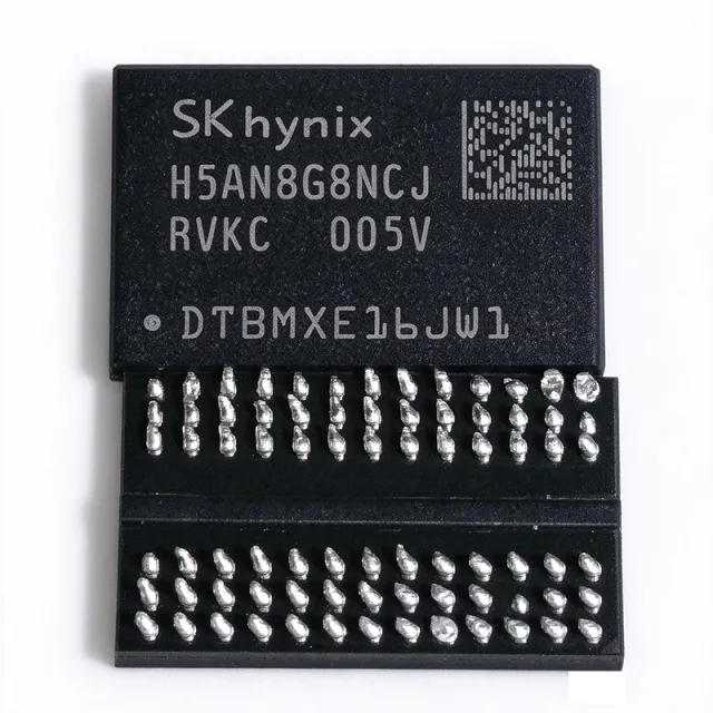
H5ANAG8NCJR-XNC - 16Gb DDR4-3200 SDRAM 2Gx8 | SK Hynix

Teilenummer: H5ANAG8NCJR-XNC ✓ Aktiv
Auf Lager Versand in 1–3 Werktagen
1.2 V Vdss FBGA-78 (7.5 x 11 mm) Package -XNC (0~95C commercial) Speed DDR4 SDRAM Memory
Ab $65.625 USD / Stück
MOQ: 1 |
Preis aktualisiert: 2026-10-13
Mengenpreise
Menge Stückpreis Gesamt
1 $112.5 $112,50
10 $81.25 $812,50
100 $71.875 $7.187,50
500 $68.75 $34.375,00
1.000 $65.625 $65.625,00
ℹ️ Alle Preise sind in USD

H5ANAG8NCJR-XNC Übersicht

The SK Hynix H5ANAG8NCJR-XNC is a 16Gb (2G x 8) DDR4 SDRAM rated for DDR4-3200 data rates, operating from a 1.2 V supply in a 78-ball FBGA (7.5 x 11 mm) package qualified for the 0C to +95C commercial temperature range.

A DDR4 SDRAM (Double Data Rate Fourth Generation Synchronous Dynamic Random Access Memory) is the mainstream volatile main-memory technology for computing systems. In the memory hierarchy, DRAM sits between CPU caches (SRAM) and persistent storage (NAND flash / SSDs), providing high-bandwidth working memory. DDR4 doubled the internal bank count of DDR3 (16 banks in 4 bank groups) and lowered the I/O voltage from 1.5 V to 1.2 V, improving bandwidth per watt. A DRAM controller inside the host SoC or memory controller manages refresh, bank interleaving, and DDR4 protocol timing, so this chip is never used standalone - it is soldered to a memory bus alongside a processor, FPGA with hard memory controller, or memory-companion chip.

Key features include 16 Gbit density per monolithic die, an x8 organization (2G addressable words x 8 bits), and DDR4-3200 operation (3200 MT/s), yielding up to 25.6 GB/s of peak bandwidth per 64-bit channel when populated 8-deep. The XNC speed grade is specified over 0C to +95C. Per TechInsights teardown analysis, the H5ANAG8NCJR-XNC contains the H5ANAG6NC die, SK hynix's first 1z nm node DRAM, offering the smallest 16Gb DDR4 die size and highest bit density (0.296 Gb/mm2) of its generation, built on non-EUV lithography.

Architecturally, DDR4 devices use a multi-bank-group array with bank-group-wise row activation, a DLL for output timing, and on-die VDDQ termination (ODT) to preserve signal integrity at 3200 MT/s. The 1z nm process shrinks the cell transistor and capacitor, reducing standby and active current versus earlier 1x/1y nm parts.

Typical applications include industrial controllers and computing modules requiring large memory density, firmware boot and embedded logging buffers, SSD controller write caches, and replacement sourcing for DDR4-based main memory on servers, workstations, and networking line cards.

Design consideration: DDR4-3200 routing requires length-matched fly-by termination and careful DQS/DQ skew budgeting; always tie CA parity and alert pins per the JEDEC DDR4 convention and your memory controller's compatibility guide.

This page synthesizes distributor pricing and stock, drop-in same-family alternatives, and practical design notes not found in the manufacturer datasheet.

Drop-in-Alternativen für H5ANAG8NCJR-XNC – gleiches Gehäuse, Pin-kompatibel. Bauteile mit anderem Gehäuse, die eine PCB-Überarbeitung erfordern, sind ausgeschlossen.

Varianten dieser Serie

Modelle derselben Serie, die drop-in-kompatibel sind mit H5ANAG8NCJR-XNC (gleiche Bauform und Footprint) – abweichend in Package, Data Rate, Interface, Organization, RoHS Status.

SK hynix
Package: FBGA-96 (96-ball)
Data Rate: 3200 Mbps/pin (DDR4-3200)
Organization: 1G x 16
Vergleichen mit H5ANAG8NCJR-XNC →
SK hynix
Package: FBGA-96
Data Rate: 3200 Mbps/pin
Interface: Parallel
Vergleichen mit H5ANAG8NCJR-XNC →
SK hynix
Package: 96-ball FBGA
Data Rate: 3200 Mbps (PC4-25600 class)
Organization: 1G x 16
Vergleichen mit H5ANAG8NCJR-XNC →
SK hynix
Package: FBGA-78
Data Rate: DDR4-2400 (2400 MT/s)
Interface: Parallel, DDR4
Vergleichen mit H5ANAG8NCJR-XNC →
SK hynix
Package: FBGA-78
Data Rate: 2666 Mbps/pin (DDR4-2666)
Vergleichen mit H5ANAG8NCJR-XNC →
SK hynix
Package: FBGA-78
Data Rate: 3200 Mbps (DDR4-3200)
Interface: Parallel
Vergleichen mit H5ANAG8NCJR-XNC →
SK hynix
Package: FBGA-78 (approximately 7.5 x 11 mm)
Organization: x8
RoHS Status: Compliant (Lead-Free & Halogen-Free per SK hynix family datasheet)
Vergleichen mit H5ANAG8NCJR-XNC →
SK hynix
Package: 78-ball FBGA
Interface: DDR4 (fully synchronous, both clock edges)
Vergleichen mit H5ANAG8NCJR-XNC →
SK hynix
Package: FBGA-78
Interface: DDR4 (JEDEC-compatible)
Vergleichen mit H5ANAG8NCJR-XNC →

Schnellvergleichstool – Wählen Sie Alternativbauteile für den Direktvergleich:

H5ANAG8NBJR-VKC

SK hynix
DDR4 SDRAM · 16 Gbit · 2G x 8 · DDR4-2666 (2666 Mbps/pin) · 1.14 V to 1.26 V (VDDQ) · 1.6 GHz (internal interface per distributor data) · 0C to +85C · FBGA-78

✓ Auf Lager

$8.6 / Stück

Datenblatt ansehen →

H5ANAG8NBJR-RDC

SK hynix
DDR4 SDRAM · 16 Gbit · 2G x 8 · 1.2 V · 1.2 V · SSTL12 · DDR4-2666 class · 78-ball FBGA

✓ Auf Lager

$3.55 / Stück

Datenblatt ansehen →

H5ANAG8NBJR-PBC

SK hynix
DDR4 SDRAM · 16 Gbit (2 GB) · x8 · 1.2 V · PBC suffix, DDR4-2666 class · FBGA-78 (7.5 mm x 11 mm) · Surface Mount · 16 banks in 4 bank groups (DDR4 standard)

✓ Auf Lager

$31.5 / Stück

Datenblatt ansehen →

H5AN8G8NCJR-XNC

SK hynix
DDR4 SDRAM · 8 Gbit · 1 Gb x 8 · 3200 Mbps (DDR4-3200) · 1.6 GHz · 1.14 V to 1.26 V (1.2 V nominal) · 78-ball FBGA, 7.5 mm x 11 mm · 0 C to +85 C

✓ Auf Lager

$30.6923 / Stück

Datenblatt ansehen →

H5ANAG8NCJR-XNC Grenzwerte & elektrische Eigenschaften

Speichertyp DDR4 SDRAM
Density 16 Gbit
Speicherorganisation 2G x 8
Datenrate 3200 MT/s (DDR4-3200)
Supply Voltage (VDD) 1.2 V
Gehäuse FBGA-78 (7.5 x 11 mm)
Betriebstemperatur 0C to +95C
Montageart Surface Mount
Process Node 1z nm (non-EUV)
Die Bit Density 0.296 Gb/mm2
Peak Bandwidth (per 64-bit channel) 25.6 GB/s at DDR4-3200
RoHS-Status Compliant
Base Part Number Family H5ANAG8NCJR (16Gb DDR4 CMOS SDRAM)
Speed Grade Suffix -XNC (0~95C commercial)

H5ANAG8NCJR-XNC fbga-78 (7.5 x 11 mm) Pinbelegungsleitfaden

Pinbelegung für H5ANAG8NCJR-XNC (fbga-78 (7.5 x 11 mm)-Gehäuse). Dieser digitale IC umfasst GPIO, Kommunikationsschnittstellen (UART, SPI, I2C) und Versorgungspins. Alternative Pin-Funktionen und Konfigurationsoptionen entnehmen Sie dem Herstellerdatenblatt. Unverzichtbar für Embedded-System-Design und PCB-Layout.

Pinbelegungsdiagramm für H5ANAG8NCJR-XNC im fbga-78 (7.5 x 11 mm)-Gehäuse

Keine detaillierten Pinbelegungsdaten verfügbar für H5ANAG8NCJR-XNC.

Siehe die Datenblatt für die vollständige Pin-Konfiguration.

Typische Anwendungen

H5ANAG8NCJR-XNC ist geeignet für 6 Anwendungs: Industrial Computing Modules, Server and Workstation Main Memory, SSD Controller Write Cache, FPGA-Based Data Acquisition and Logging, Networking Line Cards, DDR4 Replacement Sourcing and Repair.

🏭

Industrial Computing Modules

The H5ANAG8NCJR-XNC fits industrial computing modules and embedded controllers that need main memory density without DIMM sockets. Its 16Gb monolithic die in a 7.5 x 11 mm FBGA-78 delivers 2 GB per x8 device, so a 64-bit channel of eight devices reaches 16 GB while conserving board area on COM Express or SMARC carriers. DDR4-3200 operation supplies up to 25.6 GB/s per channel, sufficient for industrial vision, motion control, and protocol processing. The 0C to +95C rating covers typical enclosed industrial environments; design for the 1.2 V rail with ODT tuning per the memory controller's compatibility guide, and qualify same-family NBJR alternates for supply-chain resilience.

🖥️

Server and Workstation Main Memory

In server DIMM and memory-down designs, the H5ANAG8NCJR-XNC provides 16Gb DDR4-3200 devices for high-bandwidth main memory. A 64-bit rank of eight devices achieves 16 GB per rank at 25.6 GB/s peak bandwidth; multi-rank boards stack chip-selects for capacity scaling. The 1z nm die's 0.296 Gb/mm2 density lowers per-bit power versus 1x/1y nm predecessors, helping TDM (thermal design margins) in dense 1U servers. DDR4's bank-group architecture sustains 3200 MT/s with fly-by termination, but PCB designers must length-match DQ byte lanes within +/-25 mil class rules and follow the controller's write-leveling procedure.

💾

SSD Controller Write Cache

Enterprise and industrial SSD controllers use DDR4 DRAM as mapping-table (FTL) memory and write cache. The H5ANAG8NCJR-XNC's 2 GB per device supports large-capacity NVMe drives with multi-terabyte LBA maps, while DDR4-3200 bandwidth keeps random-write latency low. Because the FBGA-78 footprint is identical across SK hynix 8Gb/16Gb x8 family members, a single PCB layout can be populated for 4 GB (two devices) or 8 GB (four devices) cache tiers, simplifying SKU management. Ensure the SSD controller supports DDR4-3200 training, or clock down to a common speed bin; the -XNC part is backward-compatible with lower DDR4 data rates per the JEDEC DDR4 protocol.

🔧

FPGA-Based Data Acquisition and Logging

High-speed data acquisition systems built on SoC FPGAs use the H5ANAG8NCJR-XNC as streaming buffer memory for embedded logging. A 16Gb x8 device buffers gigabytes of ADC samples between bursts, and DDR4-3200 transfers clear FIFO backlogs at up to 3.2 GB/s per x8 device. Intel Arria 10-class devices (e.g., 10AS032 series) integrate hard DDR4 memory controllers that interface directly with the 1.2 V FBGA-78 device. Design attention should focus on address/command fly-by topology, ODT calibration during memory training, and refresh-borrow-aware buffering so refresh cycles do not overflow capture FIFOs at maximum sustained sample rates.

🌐

Networking Line Cards

Switch, router, and firewall line cards employ DDR4 for packet buffering, flow tables, and deep-packet-inspection state. The H5ANAG8NCJR-XNC's 2 GB density per FBGA-78 device lets designers populate 8-16 GB per card without high-layer-count memory buses, and the 1z nm process reduces standby current for always-on networking equipment. DDR4-3200 supports line-rate small-packet forwarding when paired with efficient QoS schedulers. Thermal design matters in 1U chassis: with limited airflow, derate the junction temperature using the family datasheet thermal resistance data and consider spread-spectrum clocking to manage EMI on high-speed DQ buses.

🎥

DDR4 Replacement Sourcing and Repair

For board-level repair, replacement sourcing, and shortage mitigation, the H5ANAG8NCJR-XNC serves as a direct-fit 16Gb DDR4-3200 x8 component for memory-down PCBs originally built with SK hynix FBGA-78 DDR4. Buyers should match the exact suffix (-XNC, 0-95C, DDR4-3200) where timing tables are controller-qualified, or qualify NBJR-family alternates from the same footprint for second-sourcing. The 2026 DRAM market has tightened DDR4 supply as HBM capacity expands, so replacement buyers are advised to hold buffer stock and register with multiple distributors for allocation alerts rather than sourcing single-lot spot buys.

What is the H5ANAG8NCJR-XNC?
The H5ANAG8NCJR-XNC is a SK Hynix 16Gb DDR4 SDRAM organized as 2G x 8, rated for DDR4-3200 (3200 MT/s) operation at 1.2 V in a 78-ball FBGA (7.5 x 11 mm) package over 0C to +95C. According to SK hynix family documentation, the H5ANAG4/8/6NCJR series is a monolithic 16Gb CMOS DDR4 SDRAM intended for main-memory applications requiring large density and high bandwidth.
What are the key specifications of H5ANAG8NCJR-XNC that engineers should know?
The essential facts: 16 Gbit DDR4 SDRAM, 2G x 8 organization, DDR4-3200 data rate, 1.2 V VDD, FBGA-78 package (7.5 x 11 mm), 0C to +95C commercial temperature, 1z nm process node with 0.296 Gb/mm2 die density per TechInsights. At DDR4-3200 a 64-bit channel of eight such devices delivers 25.6 GB/s peak bandwidth.
Where can I buy H5ANAG8NCJR-XNC and what is the price?
H5ANAG8NCJR-XNC is available from distributors including LCSC (in stock, from $49.12 per unit as of 2026-09-04), JLCPCB, Ampheo, and Win Source. XAIPART lists quantity pricing starting at $49.12 (qty 1), with breaks at 10, 100, 500, and 1000 pieces as of 2026-09-04. Note that 2026 DDR4 pricing is volatile due to AI-driven HBM capacity shifts, so confirm real-time quotes before ordering volume.
Is H5ANAG8NCJR-XNC in stock and what is the lead time?
Yes - LCSC lists H5ANAG8NCJR-XNC in stock, Wolfchip reported approximately 34,230 pcs as of September 2, 2026, and Octopart showed roughly 28,700 pcs as of June 15, 2026 across 9 distributors. In-stock parts typically ship within days; however, the 2026 DDR4 supply crunch means lead times for volume orders can stretch, so verify current allocation with your distributor.
What is the best drop-in replacement for H5ANAG8NCJR-XNC?
The closest same-brand drop-ins are SK hynix H5ANAG8NBJR-VKC, H5ANAG8NBJR-RDC, and H5ANAG8NBJR-PBC - all 16Gb 2G x 8 DDR4 parts in the same FBGA-78 footprint; differences are die revision and speed-bin qualification, so confirm the speed grade meets your DDR4-3200 timing budget. Note that H5AN8G8NCJR family parts are 8Gb (half density) - same package, but you need two per 16Gb position, so they are not true drop-ins.
Can a Samsung or Micron DDR4 chip replace H5ANAG8NCJR-XNC?
Cross-brand equivalents (e.g., Samsung or Micron 16Gb DDR4-3200, x8, FBGA) can be electrically compatible because all DDR4 SDRAM follow the JEDEC DDR4 standard, but you must verify three items before swapping: the exact package (78-ball FBGA land pattern match), the speed grade and its AC timing table, and your memory controller's supported SPD/DIMM validation list. Distributor cross-reference tools such as DigiKey's can shortlist candidates, but datasheet-level timing comparison remains mandatory.
H5ANAG8NCJR-XNC vs H5AN8G8NCJR-XNC - which should I choose?
They are not interchangeable: H5ANAG8NCJR-XNC is 16Gb (2G x 8) while H5AN8G8NCJR-XNC is 8Gb (1G x 8) in the same FBGA-78 package. For a new 16Gb-position design, use the AG (16Gb) part. For an 8Gb design or if you want finer granularity per chip-select, the 8Gb part works - but substituting one for the other halves or doubles your memory per rank and changes the address map.
When should I choose H5ANAG8NCJR-XNC over a lower-density DDR4 part?
Choose the 16Gb H5ANAG8NCJR-XNC when board area and component count are constrained but total memory demand is high - one 16Gb device replaces two 8Gb FBGA-78 footprints per 8-bit slice. It suits industrial computing modules, network line cards, and SSD controller buffers needing 2 GB per x8 device. If your controller supports only 8Gb ranks or you need redundant chip-selects at low density, lower-density parts are simpler to qualify.
Is H5ANAG8NCJR-XNC suitable for industrial controllers and embedded systems?
Yes. Distributor product listings explicitly position it for data storage, firmware boot, embedded logging, industrial controllers, and computing modules. The 0C to +95C commercial range covers most industrial enclosures; however, for extended -40C environments you would need an industrial grade suffix (check SK hynix grade codes) rather than the XNC commercial grade.
Where can I download the H5ANAG8NCJR-XNC datasheet PDF?
The datasheet PDF is freely available from LCSC at https://www.lcsc.com/datasheet/C22412254.pdf, and the H5ANAG8NCJR family datasheet is also listed on datasheet aggregator sites (datasheet4u, GlobalSpec). The manufacturer-family document covers H5ANAG4NCJR-xxC, H5ANAG8NCJR-xxC, and H5ANAG6NCJR-xxC 16Gb DDR4 SDRAM electrical characteristics, AC timing, and package drawings.
Where can I find the H5ANAG8NCJR-XNC pinout / ball map?
The 78-ball FBGA ball map for the x8 configuration is defined in the SK hynix H5ANAG8NCJR family datasheet package section, following the JEDEC DDR4 x8 FBGA ball assignment (DQ0-DQ7 with DQS_t/DQS_c, address/command bus, bank group inputs, power/ground balls, and VPP). Because a detailed ball-by-ball table is not reproduced in this page's verified data, download the datasheet PDF from LCSC for the authoritative ball map.
What does the -XNC speed suffix mean on SK hynix DDR4 parts?
The -XNC suffix encodes the speed grade and temperature range: XNC corresponds to DDR4-3200 class operation specified over 0C to +95C (commercial). SK hynix suffix letters differentiate speed bins and operating ranges within the same die family, so an -XNC part is not interchangeable in timing-critical designs with slower bins unless your controller de-rates the clock. Always match the suffix when qualifying alternates.
What power supply and thermal design does H5ANAG8NCJR-XNC require?
The device operates from a 1.2 V core supply per the DDR4 standard, with separate VPP and VDDQ domains defined in the family datasheet. Power scales with utilization and refresh rate; at DDR4-3200 with full bus utilization, per-device dissipation is on the order of hundreds of milliwatts, manageable with standard PCB copper pours. Follow SK hynix application guidance on VDDQ termination (ODT) settings and decoupling to keep supply ripple within DDR4 limits.
Is H5ANAG8NCJR-XNC RoHS compliant?
Yes - the JLCPCB part listing identifies H5ANAG8NCJR-XNC as RoHS compliant. Detailed REACH, halogen-free, and conflict-minerals declarations are not included in this page's verified data and should be confirmed via SK hynix product environmental documents or your distributor's compliance portal before export-controlled or consumer-regulated production.
Is H5ANAG8NCJR-XNC still in production, or should I plan a last-time buy?
The part is listed as active/in stock at multiple distributors as of September 2026. However, the broader DDR4 market is contracting as SK hynix and peers shift wafer capacity toward HBM for AI, as reported in 2026 DRAM market analyses. If this DDR4 part is on a long-lifecycle BOM, secure a multi-year supply agreement or qualified second source now rather than waiting for an official EOL notice.

Technische Referenzdaten für H5ANAG8NCJR-XNC – Vergleich, Designhinweise und Compliance-Informationen.

Auswahlhilfe

Choose the H5ANAG8NCJR-XNC when you need maximum density per 78-ball footprint: 16Gb (2 GB) per x8 device at DDR4-3200 with 0C to +95C coverage - ideal for memory-down server, industrial-module, and SSD-cache designs. Choose H5ANAG8NBJR-VKC/RDC if 16Gb density is required but NCJR stock is constrained; verify speed-bin parity first, since NBJR is an earlier die generation. Avoid H5ANAG8NBJR-PBC on DDR4-3200-qualified platforms because its suffix indicates a slower bin. Use H5AN8G8NCJR-XNC only when 8Gb granularity or lower cost per chip matters and your controller address map tolerates the halved density. For new low-power designs, LPDDR4 parts (e.g., MT53E series) offer better power efficiency but a different interface and footprint - a redesign, not a swap. Finally, in the 2026 DDR4-constrained market, dual-source across at least two of these footprints before production release.

Vergleich mit Alternativen

Parameter Dieses Produkt H5ANAG8NBJR-VKC H5ANAG8NBJR-RDC H5ANAG8NBJR-PBC H5AN8G8NCJR-XNC
Package FBGA-78 (7.5 x 11 mm) FBGA-78 (7.5 x 11 mm) - same FBGA-78 (7.5 x 11 mm) - same FBGA-78 (7.5 x 11 mm) - same FBGA-78 (7.5 x 11 mm) - same
Brand SK Hynix SK Hynix SK Hynix SK Hynix SK Hynix
Density 16 Gbit 16 Gbit 16 Gbit 16 Gbit 8 Gbit
Organization 2G x 8 2G x 8 2G x 8 2G x 8 1G x 8
Supply Voltage 1.2 V 1.2 V 1.2 V 1.2 V 1.2 V
RoHS Compliant Compliant Compliant Compliant Compliant

Wichtigste Unterscheidungsmerkmale

  • Full 16Gb density per FBGA-78 footprint (vs. H5AN8G8NCJR-XNC)
  • 1z nm node die (H5ANAG6NC) with 0.296 Gb/mm2 density (vs. H5ANAG8NBJR-VKC)
  • DDR4-3200 speed class (vs. H5ANAG8NBJR-PBC)

Designhinweise

At DDR4-3200 (3200 MT/s), signal integrity dominates the design. Use fly-by routing for address/command with per-DIMM/per-rank termination, and length-match DQ byte lanes to their DQS strobes. Set on-die termination (ODT) values during memory training rather than hard-coding, and confirm the host controller's qualified speed bin includes DDR4-3200 for the -XNC grade; otherwise clock down to a common bin.

The device runs from a 1.2 V DDR4 rail with separate VPP and VDDQ domains per the family datasheet. Estimated: at full DDR4-3200 bus utilization with 8 devices on a channel, per-device dissipation is typically on the order of 0.3-0.6 W (exact values depend on read/write mix and refresh rate - consult the datasheet IDD tables for your operating condition). Provide bulk plus per-device 0.1 uF/0.01 uF decoupling close to VDD/VDDQ balls and a solid power plane.

Do not assume all SK hynix FBGA-78 DDR4 suffixes are interchangeable: -XNC denotes DDR4-3200 class over 0C to +95C, while PBC/RDC suffixes may be slower bins. Also beware density confusion - H5AN8G8NCJR (8Gb) shares the footprint with H5ANAG8NCJR (16Gb) but halves capacity. During supply shortage, qualify alternates by datasheet AC timing comparison, not package appearance alone.

Compliance-Informationen

RoHS
Compliant
REACH
Unknown
AEC-Q100
Bleifrei
Unknown
Halogenfrei
Unknown
Konfliktmineralien
Unknown

RoHS compliance per JLCPCB part listing. REACH, halogen-free, lead-free, and conflict-minerals declarations not present in provided data - confirm via SK hynix environmental documentation.


Daten verifiziert am: 2026-09-04 – Daten geprüft und kuratiert vom Bauteil-Engineering-Team von XAIPART

Ähnliche Suchanfragen

H5ANAG8NCJR-XNC datasheet H5ANAG8NCJR-XNC price SK hynix H5ANAG8NCJR-XNC 16Gb DDR4 H5ANAG8NCJR-XNC equivalent substitute 16Gb DDR4 3200 2Gx8 FBGA-78 SDRAM H5ANAG8NCJR-XNC vs H5AN8G8NCJR-XNC H5ANAG8NCJR-XNC drop-in replacement buy H5ANAG8NCJR-XNC in stock H5ANAG8NCJR-XNC FBGA-78 pinout ball map H5ANAG8NCJR-XNC industrial controller memory Samsung Micron equivalent for H5ANAG8NCJR-XNC DDR4 3200 memory chip 0 to 95C

Verwandte Bauteile & Begriffe

SK Hynix H5ANAG8NCJR-XNC H5AN8G8NCJR-XNC H5ANAG8NBJR-VKC DDR4 SDRAM Double Data Rate 4 DRAM SDRAM FBGA-78 fine-pitch ball grid array surface mount DDR4-3200 1.2 V VDD RoHS JEDEC DDR4 standard 1z nm process node memory controller SSD write cache industrial computing module server main memory on-die termination (ODT) bank group architecture HBM capacity shift TechInsights
Schnellangebot-RFQ
Geben Sie alle Details an – unser Vertriebsteam antwortet innerhalb von 24 Stunden
Teilenummer Hersteller Gehäuse QTY Zielpreis Gesamt
Gesamt: $0.00 USD
✓
Angebotsanfrage gesendet!

Wir antworten innerhalb von 24 Stunden auf Ihre E-Mail

1
RFQ gesendet
2
Angebot erhalten
3
Bestellung aufgegeben
4
Zahlung
5
Versandt
6
Geliefert
RFQ-Details ansehen

