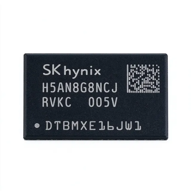
H5AN8G8NCJR-XNC - 8Gb DDR4-3200 SDRAM, x8, FBGA-78 | SK hynix
MPN: H5AN8G8NCJR-XNC ✓ Active| Qty | Unit Price | Extended |
|---|---|---|
| 1 | $52.6154 | $52.62 |
| 10 | $38 | $380.00 |
| 100 | $33.6154 | $3,361.54 |
| 500 | $32.1538 | $16,076.90 |
| 1,000 | $30.6923 | $30,692.30 |
H5AN8G8NCJR-XNC Overview
DDR4 SDRAM (Double Data Rate 4 Synchronous Dynamic Random Access Memory) is the fourth generation of the JEDEC DDR memory family. It transfers data on both rising and falling clock edges and introduces a bank-group architecture with multiple internal banks per group, allowing higher effective bandwidth than DDR3 at lower operating voltage. In the system hierarchy, it sits as main-system memory below CPU cache and above storage such as NAND flash and eMMC.
Key features of this device include fully synchronous operation referenced to both clock edges, auto self-refresh, auto precharge, an asynchronous reset function, dynamic on-chip termination (ODT), ZQ calibration, write leveling, CRC and CA parity support, and a data mask function. These capabilities simplify high-speed board design and maintain signal integrity at 3200 Mbps rates.
The XNC speed grade and its bank-group architecture allow the memory controller to issue commands to different bank groups back-to-back, maximizing effective bandwidth in mainstream DDR4-3200 channels. Low 1.2 V operation reduces power versus DDR3 at equivalent bandwidth, while per-ball power figures of approximately 30 mA and 39 mA (per LCSC/JLCPCB listing) reflect efficient dynamic and standby behavior.
Typical applications include desktop and embedded computing main memory, networking equipment line-card memory, industrial controllers, data-storage and logging subsystems, and replacement sourcing for end-of-life DRAM lines in servers and telecom platforms.
Design considerations: at DDR4-3200, fly-by routing with per-DIMM or per-component ODT calibration is essential; verify ZQ resistor placement and controller ODT settings, and confirm that the operating temperature stays within the 0 C to +85 C range or enable auto self-refresh derating above 85 C.
This page synthesizes distributor pricing, drop-in alternatives, and practical design notes not found in the manufacturer datasheet.
Drop-in alternatives for H5AN8G8NCJR-XNC — same package, pin-to-pin compatible. Different-package parts requiring PCB rework are excluded.
Variants in this series
Same-series models that are drop-in compatible with H5AN8G8NCJR-XNC (same form factor and footprint) — differing in Package, Data Rate, Interface, Organization, Supply Voltage (VDD).
Quick Comparison Tool — Select alternative parts for side-by-side comparison:
H5AN8G8NDJR-XNC
✓ In Stock
$24.5 / Unit
View Datasheet →H5AN8G8NCJR-VKC
✓ In Stock
$28.13 / Unit
View Datasheet →H5AN8G8NCJR-UHC
✓ In Stock
$2.88 / Unit
View Datasheet →H5AN8G8NCJR-RDC
✓ In Stock
$2.7 / Unit
View Datasheet →H5AN8G8NCJR-PBC
✓ In Stock
$2.4 / Unit
View Datasheet →H5AN8G8NCJR-VKI
✓ In Stock
$4.85 / Unit
View Datasheet →H5AN8G8NCJR-XNC Maximum Ratings & Electrical Characteristics
| Memory Type | DDR4 SDRAM |
| Memory Size | 8 Gbit |
| Organization | 1 Gb x 8 |
| Data Rate | 3200 Mbps (DDR4-3200) |
| Clock Frequency | 1.6 GHz |
| Supply Voltage | 1.14 V to 1.26 V (1.2 V nominal) |
| Package | 78-ball FBGA, 7.5 mm x 11 mm |
| Operating Temperature | 0 C to +85 C |
| Mounting Type | Surface Mount |
| Interface | DDR4 (8-bit data interface) |
| Architecture | Bank-group based DDR4 |
| Refresh | Auto self-refresh |
| Precharge | Auto precharge |
| On-Chip Termination | Dynamic ODT |
| Calibration | ZQ calibration, write leveling |
| Error Handling | CRC function |
| Reset | Asynchronous reset |
| Data Mask | Data mask function |
| Current - Operating | 39 mA |
| Current - Standby | 30 mA |
| RoHS Status | Compliant |
| Lead-Free / Halogen-Free | Yes |
H5AN8G8NCJR-XNC 78-ball fbga, 7.5 mm x 11 mm Pin Configuration Guide
Pin configuration for H5AN8G8NCJR-XNC (78-ball fbga, 7.5 mm x 11 mm package). This digital IC includes GPIO, communication interfaces (UART, SPI, I2C), and power pins. Refer to the manufacturer datasheet for alternate pin functions and configuration options. Essential for embedded system design and PCB layout.

No detailed pinout data available for H5AN8G8NCJR-XNC.
Refer to the datasheet for full pin configuration.
Typical Applications
H5AN8G8NCJR-XNC is suitable for 6 applications: Desktop and Embedded Computing Main Memory, Networking Equipment Line-Card Memory, Industrial Controllers and Automation Systems, Data Storage, Logging, and Firmware Boot Systems, Replacement Sourcing for DDR4 End-of-Life Lines, Embedded Vision and Display Processing Boards.
Desktop and Embedded Computing Main Memory
The H5AN8G8NCJR-XNC serves as main-system memory in desktop motherboards, mini-PCs, and embedded computing modules, where its 8 Gb density and DDR4-3200 data rate provide 3200 Mbps per-pin bandwidth over an 8-bit data interface. Connected in a fly-by or point-to-point topology to a memory controller supporting DDR4-3200, it delivers high bandwidth at a low 1.2 V supply. Features like write leveling, ZQ calibration, and dynamic ODT maintain signal integrity across DDR4-3200 speeds, while auto self-refresh preserves memory content during low-power idle states. Component-level (non-DIMM) DDR4 designs benefit from the compact 7.5 mm x 11 mm FBGA-78 footprint that fits dense CPU-adjacent layouts.
Recommended
Networking Equipment Line-Card Memory
Routers, switches, and network appliances use the H5AN8G8NCJR-XNC as packet-buffer and control-plane memory. Its DDR4-3200 throughput supplies the bandwidth needed to service multi-gigabit packet streams, and the CRC function plus CA parity help detect bus errors in electrically noisy chassis environments. The asynchronous reset function allows the system controller to re-initialize the DRAM quickly after a fault, and auto precharge reduces command overhead in random-access buffer patterns. The 0 C to +85 C range and dynamic ODT termination support central-office and enterprise equipment temperature profiles without external termination complexity.
Recommended
Industrial Controllers and Automation Systems
Industrial PLCs, motion controllers, and machine-vision hosts deploy the H5AN8G8NCJR-XNC for program and data memory. The 8 Gb x8 organization simplifies error-correcting code design with a single device per byte lane, while ZQ calibration and on-chip termination keep DDR4-3200 signaling robust across factory temperature swings within the 0 C to +85 C range. Auto self-refresh protects data during controller-initiated low-power windows, and the CRC function improves data-path reliability in EMI-rich environments near drives and inverters. Sourcing stability matters in industrial platforms with long service lives, so the VKI industrial-grade sibling offers an extended-lifecycle drop-in on the same FBGA-78 footprint.
Recommended
Data Storage, Logging, and Firmware Boot Systems
Storage controllers, SSD bridge boards, and embedded logging devices use the H5AN8G8NCJR-XNC as working memory for caching, wear-leveling tables, and firmware execution. Per the datasheet family overview (DigChip), the NCJR series is suited to main-memory applications requiring large density and high bandwidth; in storage, the 8 Gb capacity comfortably holds multi-gigabyte logical-to-physical mapping caches. DDR4-3200 operation shortens cache lookup and RAID XOR computation times, while auto self-refresh preserves mapping metadata through power-loss-event handling sequences. The compact 78-ball FBGA-78 package allows multiple devices to be placed around a storage ASIC with fly-by routing.
Recommended
Replacement Sourcing for DDR4 End-of-Life Lines
As DRAM vendors consolidate DDR4 production toward newer nodes, system builders maintaining legacy servers, telecom platforms, and test equipment need assured replacement sources. The H5AN8G8NCJR-XNC retains strong channel stock (28,100-30,520 pcs reported as of Aug 31, 2026) and offers same-footprint family alternatives (NDJR die revision, VK/UH/RD/PB speed grades) that drop onto the identical FBGA-78 land pattern, simplifying BOM continuity. Cross-brand JEDEC-standard DDR4 x8 devices such as the Micron MT40A1G8 series implement the same ballout for qualified second sourcing. Procurement teams should pair channel stock checks with a validated second source before the final-time-buy window.
Recommended
Embedded Vision and Display Processing Boards
Camera modules, video analytics nodes, and display processors require frame-buffer bandwidth that scales with resolution. The H5AN8G8NCJR-XNC provides 3200 Mbps x 8-bit data transfer per device, enabling sustained 4K frame buffering and concurrent processing workloads when multiple devices form a 32-bit or 64-bit DDR4 channel. Write leveling and dynamic ODT simplify high-speed routing across the board, and the 1.2 V operation helps meet thermal budgets in fanless vision systems within the 0 C to +85 C envelope. For space-constrained module designs, the AFR-package siblings in the same 8 Gb family offer a more compact footprint with the same DDR4-3200 capability.
Recommended
Recommended Products Summary
Engineering reference data for H5AN8G8NCJR-XNC — comparison, design guidance, and compliance information.
Selection Guide
Comparison with Alternatives
| Parameter | This Product | H5AN8G8NDJR-XNC | H5AN8G8NCJR-VKC | H5AN8G8NCJR-UHC |
|---|---|---|---|---|
| Package | 78-ball FBGA (7.5 x 11 mm) | 78-ball FBGA - same | 78-ball FBGA - same | 78-ball FBGA - same |
| Brand | SK Hynix | SK Hynix | SK Hynix | SK Hynix |
| Density / Organization | 8 Gb, 1 Gb x 8 | 8 Gb, 1 Gb x 8 | 8 Gb, 1 Gb x 8 | 8 Gb, 1 Gb x 8 |
| Data Rate | 3200 Mbps (DDR4-3200) | 3200 Mbps (DDR4-3200) | DDR4-2666 class (VK) | DDR4-2400 class (UH) |
| Supply Voltage | 1.14 V - 1.26 V | 1.14 V - 1.26 V | 1.14 V - 1.26 V | 1.14 V - 1.26 V |
| Operating Temperature | 0 C to +85 C | 0 C to +85 C | 0 C to +85 C | Industrial grade (VKI) |
| Die Generation | NCJR (CJR die) | NDJR (DJR die) - newer revision | NCJR (CJR die) | NCJR (CJR die) |
| Key Features | Auto self-refresh, dynamic ODT, ZQ cal, write leveling, CRC, async reset | Same JEDEC DDR4 feature set | Same JEDEC DDR4 feature set | Same JEDEC DDR4 feature set |
| RoHS / Lead-Free | Compliant / Yes | Compliant / Yes | Compliant / Yes | Compliant / Yes |
Key Differentiators
- Full DDR4-3200 bandwidth in the CJR family (vs H5AN8G8NCJR-VKC)
- Same-footprint die-revision migration path (vs H5AN8G8NDJR-XNC)
- Industrial screening option in family (vs H5AN8G8NCJR-VKI)
- Trade-off: speed over cost and margin (vs H5AN8G8NCJR-UHC)
Design Notes
At DDR4-3200, signal integrity dominates success or failure. Route address/command as a fly-by (daisy-chain) topology with on-chip termination, and match DQS/DQS# pair skew within the datasheet timing windows. Use dynamic ODT and ZQ calibration via the dedicated ZQ ball with an external precision resistor (typically 240 ohm, per JEDEC DDR4 practice) placed within millimeters of the ball. Simulate SI at 1.6 GHz with IBIS models from SK hynix before fabrication, and budget for controller write-leveling to compensate flight-time skew across multiple devices.
Design the VDD/VDDQ rails for 1.2 V nominal (1.14 V - 1.26 V tolerance) with low-ESR bulk and per-ball ceramic decoupling (e.g., multiple 0.1 uF plus 1 uF capacitors adjacent to the FBGA). Listed dynamic current is approximately 39 mA with 30 mA standby per device, but simultaneous switching of 8 DQ lines at 3200 Mbps creates high di/dt transients; a solid power plane and local decoupling are mandatory to avoid core-noise-induced refresh errors.
The commercial 0 C to +85 C operating range requires derating above 85 C ambient: per standard DDR4 practice, extend refresh rate (auto self-refresh with 2x refresh) above the normal-temperature limit. Estimated: at 8 DQ lines switching at 3200 Mbps, dynamic power in the hundreds of milliwatts range per device can raise FBGA junction temperature several tens of degrees above ambient in sealed enclosures - verify with thermal simulation and consider copper pours under the package.
Do not interchange 8 Gb and 16 Gb devices (e.g., H5ANAG8NCJR-XNC) without updating the controller address map - the density difference changes bank/row addressing even though the FBGA-78 footprint is shared. Always re-run memory training (write leveling, read training, ODT re-tuning) after any second-source swap, and confirm the exact speed-grade suffix (XN vs VK vs UH) matches controller timing registers; a VK-grade part will not reliably run 3200 Mbps timings.
Compliance Information
RoHS compliant and Lead-Free & Halogen-Free per JLCPCB listing and Alldatasheet family document (H5AN8G8NCJR-XXC). REACH and conflict-minerals declarations not present in verified data.



