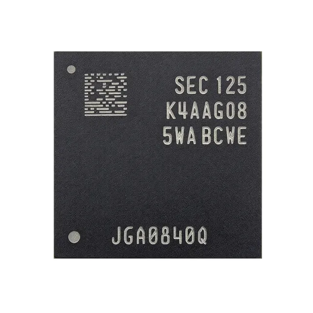
K4A8G085WB-BCWE - 8Gb DDR4 SDRAM 3200Mbps | Samsung
Référence : K4A8G085WB-BCWE ✓ Actif| Qté | Prix unitaire | Total |
|---|---|---|
| 1 | $21.0938 | $21,09 |
| 10 | $15.2344 | $152,34 |
| 100 | $13.4766 | $1 347,66 |
| 500 | $12.8906 | $6 445,30 |
| 1 000 | $12.3047 | $12 304,70 |
K4A8G085WB-BCWE Présentation
DDR4 SDRAM (Double Data Rate 4 Synchronous Dynamic Random Access Memory) is the fourth generation of DDR memory technology, sitting within the broader memory hierarchy of volatile semiconductor memory (DRAM -> DDR SDRAM -> DDR4 -> GDDR/LPDDR variants). Compared with DDR3, DDR4 reduces operating voltage from 1.5V to 1.2V (roughly 25% lower power per Samsung) and increases bank groups, prefetch efficiency, and per-pin data rates up to 3200 Mbps.
Key features include the 1G x 8 organization suited to single-rank and multi-rank DIMM or on-board memory designs, 3200 Mbps maximum data rate for high-bandwidth applications, a low 1.2V core supply for reduced power consumption, and the compact 78-ball FBGA surface-mount package for space-constrained embedded designs. Samsung's B-die devices are also noted for their tight timing characteristics.
Technically, the device uses an 8n prefetch architecture with bank groups, on-die termination (ODT), and DLL-based timing control. Setup/hold specifications include VREF AC-noise derating of up to +/-1% of VDD, per the Samsung datasheet, ensuring signal integrity at high data rates on fly-by or pointed-topology DDR4 buses.
Typical applications include servers and data-center memory modules, industrial controllers, network communication equipment, embedded computing modules, firmware boot and data-logging subsystems, and high-performance desktop memory upgrades.
Design consideration: the BCWE grade is specified for 0C to +85C; industrial-temperature designs should verify the BI-grade variants, and controller timing registers must be programmed for the exact speed bin.
This page synthesizes distributor pricing, drop-in alternatives, procurement notes, and practical design guidance not found in the manufacturer datasheet.
Alternatives de remplacement direct pour K4A8G085WB-BCWE — même boîtier, compatible broche à broche. Les références à boîtier différent nécessitant une retouche du PCB sont exclues.
Variantes de cette série
Modèles de la même série directement compatibles avec K4A8G085WB-BCWE (même facteur de forme et même empreinte) — différant par Package, Density, Mounting Type, Organization, Data Rate.
Outil de comparaison rapide — sélectionnez des références alternatives pour une comparaison côte à côte :
K4A8G085WB-BCTD
✓ En stock
$7.5 / unité
Voir la fiche technique →K4A8G085WB-BCRC
✓ En stock
$6.8 / unité
Voir la fiche technique →K4A8G085WB-BCPB
✓ En stock
$13.7813 / unité
Voir la fiche technique →K4A8G085WC-BCWE
✓ En stock
$7.3828 / unité
Voir la fiche technique →K4A8G085WC-BIWE
✓ En stock
$6.29 / unité
Voir la fiche technique →K4A8G085WB-BCWE Valeurs maximales et caractéristiques électriques
| Type de mémoire | DDR4 SDRAM |
| Density | 8 Gb |
| Organisation de la mémoire | 1G x 8 |
| Débit de données | 3200 Mbps |
| Supply Voltage (VDD) | 1.2 V |
| Température de fonctionnement | 0C to +85C |
| Boîtier | 78-ball FBGA |
| Type de montage | Surface Mount |
| Die Classification | B-die |
| Interface | DDR4 (SSTL12) |
| Application Domain | Server, industrial control, networking, embedded systems |
| VREF AC-Noise Derating | +/-1% of VDD included in timing deratings |
Guide de configuration des broches du K4A8G085WB-BCWE 78-ball fbga
Configuration des broches du K4A8G085WB-BCWE (boîtier 78-ball fbga). Ce circuit intégré numérique comprend des GPIO, des interfaces de communication (UART, SPI, I2C) et des broches d'alimentation. Consultez la fiche technique du fabricant pour les fonctions alternatives des broches et les options de configuration. Indispensable pour la conception de systèmes embarqués et la conception de circuits imprimés.

Aucune donnée de brochage détaillée disponible pour K4A8G085WB-BCWE.
Consultez la fiche technique pour la configuration complète des broches.
Applications typiques
K4A8G085WB-BCWE convient pour 6 applications: Server Memory Subsystems, Industrial Controllers, Network Communication Equipment, Embedded Computing Modules, Firmware Boot and Data Logging, High-Performance Desktop Memory.
Server Memory Subsystems
The K4A8G085WB-BCWE's 8Gb density and 3200 Mbps data rate make it well suited to server DRAM subsystems, whether assembled into RDIMM/LRDIMM modules or soldered directly on server boards. The 1G x 8 organization allows wide 64-bit or 72-bit ECC bus construction with 8 or 9 devices per rank, and 1.2V operation reduces per-rank power compared with DDR3, cutting thermal load in dense chassis. Samsung's DDR4 bank-group architecture sustains high sequential bandwidth for virtualization and database workloads. Designers should configure the memory controller's timing registers for the WE 3200 Mbps speed bin and apply fly-by routing with per-DIMM termination. As of 2026-09-04, verify availability since DDR4 is in market end-of-cycle.
Recommandé
Industrial Controllers
Industrial PLCs, motion controllers, and edge gateways benefit from the K4A8G085WB-BCWE's 8Gb capacity for buffering sensor data, running local control loops, and hosting embedded Linux images. The 0C to +85C commercial range suits indoor cabinets and enclosed controllers; for extended-temperature deployments, the pin-compatible K4A8G085WC-BIWE industrial grade drops into the same 78-ball FBGA footprint with zero PCB redesign. The 1.2V rail simplifies integration with standard industrial power trees, and the x8 organization keeps DRAM controller routing simple on 4-6 layer boards. Memory training should be rerun after any die-revision substitution to validate timing margins across the full temperature range.
Recommandé
Network Communication Equipment
Routers, switches, and 5G network appliances use DDR4 for packet buffering, route tables, and control-plane software. The K4A8G085WB-BCWE provides 3200 Mbps per pin, and a 32-bit bus of four devices delivers 12.8 GB/s peak bandwidth, enough for line-rate buffering in access and aggregation equipment. The compact 78-ball FBGA allows dense DRAM placement next to network processors on space-constrained line cards. Samsung's VREF AC-noise derating methodology (up to +/-1% of VDD) guides signal-integrity budgeting for the multi-drop DDR4 bus. Always confirm the speed bin against the network processor's supported DDR4 rate list before design freeze.
Recommandé
Embedded Computing Modules
COMs (computer-on-modules) and SBCs solder the K4A8G085WB-BCWE directly to the carrier to avoid SO-DIMM connectors, saving height and improving vibration reliability. One or two 8Gb devices give 1-2 GB of system RAM, sufficient for real-time Linux, HMI stacks, and edge inference frameworks. The x8 organization matches the 16/32-bit DDR controllers common in embedded SoCs, and 3200 Mbps operation supports bandwidth-hungry graphics and vision pipelines. Because the B-die device was widely qualified across embedded SoC platforms, BSP timing tables are broadly available. For wide-temperature modules, substitute the BI-grade pin-compatible part during the design phase rather than after qualification.
Recommandé
Firmware Boot and Data Logging
The K4A8G085WB-BCWE serves as execution memory for bootloader decompression, kernel staging, and high-rate data-logging buffers in test instruments and telemetry recorders. Its 3200 Mbps rate sustains sustained write streams from high-speed ADCs or camera interfaces, and the 8Gb depth allows long capture windows before offload. Typical architectures boot from SPI NOR (e.g., Macronix or Winbond serial flash) into DDR4, then run the application entirely from DRAM. Designers should enable controller ECC where supported to protect long-duration logging sessions against soft errors, and should verify refresh configuration (including temperature-compensated refresh) matches Samsung datasheet recommendations for the operating environment.
Recommandé
High-Performance Desktop Memory
Enthusiast and workstation UDIMMs built on Samsung B-die components such as the K4A8G085WB-BCWE are prized for tight timing headroom at and above the DDR4-3200 JEDEC bin. Eight x8 devices populate a 64-bit unbuffered DIMM for 8 GB capacity, and B-die's known characteristics make it a predictable choice for custom timing profiles. For consumer designs, the 0C to +85C range and 1.2V standard supply align with desktop platform requirements. Note that B-die supply is tightening as the industry transitions to DDR5; procurement teams designing replacement modules should qualify the WC-die BCWE as a second source and validate memory training profiles on both die revisions before release.
Recommandé
Récapitulatif des produits recommandés
Données de référence d'ingénierie pour K4A8G085WB-BCWE — comparaison, recommandations de conception et informations de conformité.
Guide de sélection
Comparaison avec les alternatives
| Paramètre | Ce produit | K4A8G085WB-BCTD | K4A8G085WB-BCRC | K4A8G085WB-BCPB | K4A8G085WC-BCWE | K4A8G085WC-BIWE |
|---|---|---|---|---|---|---|
| Package | 78-ball FBGA | 78-ball FBGA - same | 78-ball FBGA - same | 78-ball FBGA - same | 78-ball FBGA - same | 78-ball FBGA - same |
| Brand | Samsung Electronics | Samsung Electronics | Samsung Electronics | Samsung Electronics | Samsung Electronics | Samsung Electronics |
| Density | 8 Gb | 8 Gb | 8 Gb | 8 Gb | 8 Gb | 8 Gb |
| Organization | 1G x 8 | 1G x 8 | 1G x 8 | 1G x 8 | 1G x 8 | 1G x 8 |
| Die Revision | B-die | B-die | B-die | B-die | C-die | C-die |
| Supply Voltage | 1.2 V | 1.2 V | 1.2 V | 1.2 V | 1.2 V | 1.2 V |
| Substitution Risk | Reference part | Low (same die) | Low (same die, verify speed) | Low (same die, verify speed) | Medium (timing differences reported) | Medium (C-die timing, industrial temp benefit) |
Principaux différenciateurs
- Native DDR4-3200 WE speed bin (vs K4A8G085WB-BCPB)
- B-die characterization depth (vs K4A8G085WC-BCWE)
- Commercial temperature optimization (vs K4A8G085WC-BIWE)
Notes de conception
Route the DDR4 bus using fly-by topology for address/command with on-die termination (ODT) enabled, and length-match data groups per Samsung's layout guidelines. Samsung's datasheet explicitly includes VREF AC-noise of up to +/-1% of VDD within timing deratings, so keep VREF decoupling close to the FBGA balls and isolate VREF planes from high-di/dt return paths. At 3200 Mbps, target controlled impedance and simulate eye margins on the longest DQS/DQ nets before fab.
Provide a dedicated 1.2V rail for VDD with bulk capacitance at the point of load plus high-frequency ceramic decoupling at each FBGA power ball pair. Estimated: a single 8Gb device at 3200 Mbps draws on the order of several hundred milliamps during active bursts; size the regulator for the full rank's simultaneous switching rather than a single device. Do not share the VDD rail with noisy switching loads; VREF sensitivity to AC noise is explicitly captured in Samsung's timing derating model.
Do not assume suffix equivalence within the K4A8G085W family. The B-to-C die change (WB to WC) introduces timing differences per published compatibility reviews, and TD/RC/PB suffixes denote different speed bins. Always decode the full ordering code against Samsung's ordering-information table, reconfigure controller timing registers for the installed bin, and rerun memory training and stress tests after any second-source substitution. For 0-85C designs, do not substitute industrial BI parts without updating qualification documentation.
Informations de conformité
Compliance statements were not present in the retrieved web data; consult the official Samsung product page or environmental data sheet for RoHS/REACH status.