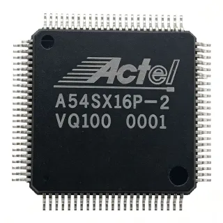
A54SX16-2VQG100I - 24K Gate SX FPGA, 81 I/O | Microsemi
MPN: A54SX16-2VQG100I ✓ Active| Qty | Unit Price | Extended |
|---|---|---|
| 1 | $42.5 | $42.50 |
| 10 | $39.2 | $392.00 |
| 100 | $35.8 | $3,580.00 |
| 500 | $32.4 | $16,200.00 |
| 1,000 | $29.9 | $29,900.00 |
A54SX16-2VQG100I Overview
An FPGA (Field-Programmable Gate Array) is a semiconductor device containing programmable logic blocks and interconnects that designers configure after manufacturing. Within the programmable logic hierarchy, the device-level path runs: FPGA -> programmable logic device -> digital IC -> semiconductor. The Actel SX family uses a sea-of-modules architecture with a fine-grained logic module array, which delivers ASIC-like gate efficiency and high system clock rates (up to 320 MHz toggle frequency per distributor data) without the configuration memory of SRAM FPGAs.
Key features include 0.35 um CMOS antifuse technology that is non-volatile and live-at-power-up, 1452 logic array blocks (LABs), dual 3.3 V / 5 V supply operation for mixed-voltage system integration, and 81 configurable I/O supporting common single-ended standards. The antifuse programming method produces no configuration bitstream to load, reducing boot complexity and offering inherent resistance to configuration readback.
Architecturally, the SX sea-of-modules structure places combinational and sequential logic modules in a dense regular array, minimizing routing delays and enabling deterministic, performance-intensive designs at low power compared to SRAM-based alternatives.
Typical applications include industrial control and automation logic, communications and networking glue logic, aerospace and defense system controllers, and bridge/sequencing functions in embedded systems where instant-on behavior matters.
Design consideration: because antifuse devices are one-time programmable, verify the design thoroughly in simulation before programming; also budget for the dual supply rails required by this part.
This page consolidates distributor pricing tiers, drop-in same-package alternatives, design notes, and FAQ content not found together on the manufacturer datasheet page.
Drop-in alternatives for A54SX16-2VQG100I — same package, pin-to-pin compatible. Different-package parts requiring PCB rework are excluded.
Variants in this series
Same-series models that are drop-in compatible with A54SX16-2VQG100I (same form factor and footprint) — differing in Family, Operating Temperature, System Gates, Process Technology, Speed Grade.
Quick Comparison Tool — Select alternative parts for side-by-side comparison:
A54SX16-1VQG100I
✅ Drop-In✓ In Stock
$31.9 / Unit
View Datasheet →A54SX16-1VQG100
✅ Drop-In✓ In Stock
$31.5 / Unit
View Datasheet →A54SX16-2VQG100
✅ Drop-In✓ In Stock
$48.9 / Unit
View Datasheet →A54SX16-VQG100I
✅ Drop-In✓ In Stock
Contact for price
View Datasheet →A54SX16P-1VQG100I
✅ Drop-In✓ In Stock
$1870.24 / Unit
View Datasheet →A54SX16-2VQG100I Maximum Ratings & Electrical Characteristics
| Series | SX (Actel SX family) |
| Number of Gates | 24000 |
| Number of Logic Cells | 924 |
| Number of LABs/CLBs | 1452 |
| Number of I/O | 81 |
| Supply Voltage - Core | 3 V ~ 3.6 V |
| Supply Voltage - I/O | 4.75 V ~ 5.25 V |
| Maximum Frequency | 320 MHz |
| Process Technology | 0.35 um CMOS |
| Programmable Type | Antifuse (one-time programmable) |
| Speed Grade | -2 |
| Package / Case | 100-TQFP (VQFP, 14x14 mm) |
| Mounting Type | Surface Mount |
| Operating Temperature | -40C to +85C (Industrial, I suffix) |
A54SX16-2VQG100I 100-tqfp (vqfp, 14x14 mm) Pin Configuration Guide
Pin configuration for A54SX16-2VQG100I (100-tqfp (vqfp, 14x14 mm) package). This digital IC includes GPIO, communication interfaces (UART, SPI, I2C), and power pins. Refer to the manufacturer datasheet for alternate pin functions and configuration options. Essential for embedded system design and PCB layout.

No detailed pinout data available for A54SX16-2VQG100I.
Refer to the datasheet for full pin configuration.
Typical Applications
A54SX16-2VQG100I is suitable for 6 applications: Industrial Control and Automation Logic, Communications and Networking Glue Logic, Aerospace and Defense Ground Systems, ASIC Prototyping and Bridge Logic, Mixed-Voltage System Power Sequencing and Supervision, Test and Measurement Instrumentation.
Industrial Control and Automation Logic
The A54SX16-2VQG100I fits industrial control because its 24,000 antifuse gates and 81 I/O integrate sequencers, address decoders, and bus interfaces that previously required multiple 5 V TTL devices. Its dual supply architecture (3.0-3.6 V core, 4.75-5.25 V I/O) lets it sit directly on legacy 5 V industrial backplanes while running 3.3 V internal logic. The industrial -40C to +85C rating covers unconditioned factory-floor enclosures, and instant-on antifuse configuration means PLC I/O modules are active the moment power is applied, with no configuration load time. Deterministic -2 speed-grade timing simplifies worst-case response analysis for safety-adjacent interlock logic.
Recommended
Communications and Networking Glue Logic
In telecom and networking line cards, the A54SX16-2VQG100I consolidates address decoding, interrupt control, and data-path multiplexing into one 24,000-gate device. The SX family's sea-of-modules architecture delivers the fine-grained, ASIC-like routing density that bus-arbitration and framing logic needs, and distributor data quotes operation up to 320 MHz in the -2 grade, sufficient for high-throughput state machines. Because antifuse configuration is non-volatile, line cards initialize instantly after hot-swap power events, avoiding SRAM FPGA configuration-fetch delays. The 100-TQFP with 81 I/O provides ample pin count for 8/16-bit peripheral buses while keeping board area at the 14x14 mm footprint.
Recommended
Aerospace and Defense Ground Systems
Defense ground equipment and avionics support racks benefit from the A54SX16-2VQG100I's antifuse technology: the programmed configuration contains no SRAM bits to upset, corrupt, or read back, reducing configuration-integrity concerns in secure systems. The device powers up functional immediately, which matters for watchdog and power-sequencing controllers that must supervise other rails from the first milliseconds. With 24,000 gates and 81 industrial-rated I/O, it implements MIL-STD-style discrete I/O conditioning, PWM generators, and voter logic. Note that this specific I-grade part is commercial-industrial, not radiation-tolerant; space programs should use the RTAX family.
Recommended
ASIC Prototyping and Bridge Logic
The SX16's sea-of-modules architecture was widely used to prototype and substitute small gate arrays: 24,000 gates of fine-grained combinational and sequential modules map ASIC-style netlists with predictable utilization. Engineers use the A54SX16-2VQG100I as a bridge device between microprocessors and custom peripherals during ASIC development, exploiting the 0.35 um process's 5 V-tolerant I/O to match legacy chip sets. Because antifuse parts are one-time programmable, teams typically validate on the -1 grade or in simulation before committing -2 parts. The 100-TQFP package allows quick-turn test boards with standard surface-mount assembly.
Recommended
Mixed-Voltage System Power Sequencing and Supervision
Systems combining 5 V and 3.3 V domains use the A54SX16-2VQG100I as a sequencing supervisor: the 5 V I/O rail (4.75-5.25 V) monitors and controls 5 V devices while the 3.3 V core tracks the low-voltage domain. Antifuse instant-on behavior is the decisive parameter here - the logic is valid within microseconds of power application, before SRAM FPGAs can even load configuration, so reset distribution and enable sequencing are guaranteed from the first cycle. The 81 I/O provide fanout for multiple enable lines, power-good monitors, and fault latches, and deterministic -2 timing supports precise interlock timing analysis across the -40C to +85C industrial range.
Recommended
Test and Measurement Instrumentation
Bench and automated test instruments use the A54SX16-2VQG100I for timing generation, counter/timer arrays, and stimulus formatting. The fine-grained SX architecture builds ripple-carry counters and shift registers with ASIC-like density, and the -2 speed grade's delay cells support precise edge placement for stimulus hardware. The 81 I/O drive relay matrices, level shifters, and front-panel interfaces, mixing 5 V legacy instrument buses with 3.3 V controller domains thanks to the dual supply specification. Non-volatile antifuse configuration means an instrument is functional at power-up for calibration-critical warm-up sequences, with no configuration image stored in external flash to verify.
Recommended
Recommended Products Summary
Engineering reference data for A54SX16-2VQG100I — comparison, design guidance, and compliance information.
Selection Guide
Comparison with Alternatives
| Parameter | This Product | A54SX16-1VQG100I | A54SX16-2VQG100 | A54SX16-VQG100I | A54SX16P-1VQG100I |
|---|---|---|---|---|---|
| Package | 100-TQFP (VQFP, 14x14 mm) | 100-TQFP (VQFP, 14x14 mm) - same | 100-TQFP (VQFP, 14x14 mm) - same | 100-TQFP (VQFP, 14x14 mm) - same | 100-TQFP (VQFP, 14x14 mm) - same |
| Brand | Microsemi (Microchip) | Microsemi (Microchip) | Microsemi (Microchip) | Microsemi (Microchip) | Microsemi (Microchip) |
| Number of Gates | 24000 | 24000 | 24000 | 24000 | 24000 (SX16P die) |
| Number of I/O | 81 | 81 | 81 | 81 | 83 |
| Speed Grade | -2 | -1 (slower) | -2 (same) | standard | -1 (SX16P timing) |
| Operating Temperature | -40C to +85C (Industrial) | -40C to +85C (Industrial) | 0C to +70C (Commercial) | -40C to +85C (Industrial) | -40C to +85C (Industrial) |
| Programmable Technology | Antifuse (0.35 um CMOS) | Antifuse (0.35 um CMOS) | Antifuse (0.35 um CMOS) | Antifuse (0.35 um CMOS) | Antifuse (SX-A family) |
Key Differentiators
- Faster -2 speed grade (vs A54SX16-1VQG100I)
- Industrial temperature range (vs A54SX16-2VQG100)
- Instant-on non-volatile antifuse configuration (vs SRAM FPGAs (e.g., A3PE600 requires reprogramming flow differences))
Design Notes
The A54SX16-2VQG100I requires two independent supply rails: 3.3 V (3.0-3.6 V) for core logic and 5 V (4.75-5.25 V) for I/O. Estimated: at typical SX16 operating currents (tens of mA core), a small LDO or buck converter per rail suffices, but decouple each rail at the package with at least 0.1 uF ceramic plus 10 uF bulk. Verify rail sequencing requirements in the 54SX family datasheet before applying both supplies, and ensure the 5 V rail never back-powers the 3.3 V domain through I/O structures.
Antifuse FPGAs are one-time programmable - an incorrect or marginal design cannot be reworked on the same device. Complete full functional simulation and post-layout timing simulation with -2 speed-grade libraries in the Microchip Libero/Designer flow before releasing devices to programming. Budget programming yield: order extra blank devices (typically 5-10%) because a programming failure renders the part scrap. Never substitute commercial-grade (no I suffix) parts into industrial assemblies without requalifying timing across the full -40C to +85C range.
The 14x14 mm 100-TQFP has 0.5 mm pin pitch; design land patterns to the manufacturer mechanical drawing in the 54SX datasheet, with slightly elongated pads to aid solder inspection. Keep unused I/O configured per the datasheet recommendation (inputs with pull-up/down or tied levels) to avoid floating-node noise. Route high-fanout clocks on inner layers with short stubs; the sea-of-modules architecture allows multiple clock resources, so assign clocks deliberately in the place-and-route constraints rather than leaving default routing.
Estimated: at moderate core current (tens of mA from 3.3 V, under 200 mW typical for SX16 designs), junction temperature rise in the 100-TQFP remains well within the industrial rating even at +85C ambient. However, designs heavily populating 81 I/O with 5 V loads can push total dissipation toward several hundred milliwatts; compute actual I/O current per pin against datasheet limits and verify theta_JA from the package drawing section of the family datasheet before finalizing enclosure derating.
Compliance Information
Compliance status not stated in provided web data for this legacy Microsemi SX device; confirm with Microchip product compliance documentation before export-controlled or RoHS-restricted builds.