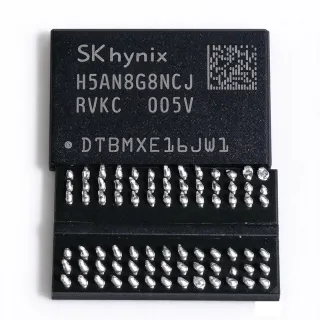
H5AN8G8NDJR-XNC - 8Gb DDR4-3200 SDRAM | SK Hynix
MPN: H5AN8G8NDJR-XNC ✓ Active| Qty | Unit Price | Extended |
|---|---|---|
| 1 | $31.28 | $31.28 |
| 10 | $29.5 | $295.00 |
| 100 | $27.8 | $2,780.00 |
| 500 | $26.1 | $13,050.00 |
| 1,000 | $24.5 | $24,500.00 |
H5AN8G8NDJR-XNC Overview
DDR4 SDRAM (Double Data Rate 4 Synchronous Dynamic Random-Access Memory) is a type of volatile memory that transfers data on both rising and falling edges of the clock signal, effectively doubling the data rate. It is the successor to DDR3 and offers higher speed, lower power consumption, and increased density. DDR4 operates at a lower voltage (1.2V) compared to DDR3 (1.5V), reducing power consumption by up to 40%. It is a critical component in modern computing systems, serving as the main memory for CPUs, GPUs, and SoCs, and is part of the memory hierarchy that includes cache, main memory, and storage.
Key features of the H5AN8G8NDJR-XNC include a bank group-based internal architecture that enhances performance, support for standard DDR4 features such as auto self-refresh, auto precharge, asynchronous reset, data mask, dynamic on-chip termination (DTC), ZQ calibration, write leveling, and CRC (Cyclic Redundancy Check) for data integrity. The device also supports on-die ECC (Error Correction Code) in some configurations, though this specific part is a standard non-ECC variant. The 78-ball FBGA package is optimized for high-density PCB layouts, and the device is available in tray packaging.
Technically, the H5AN8G8NDJR-XNC implements a 16n prefetch architecture, which is standard for DDR4, allowing it to achieve high bandwidth with a relatively low clock frequency. The device supports a burst length of 8 (BL8) and can be configured for burst chop (BC4). It also supports various power-saving modes, including active power-down, precharge power-down, and self-refresh, which are essential for mobile and embedded applications where power efficiency is critical. The device is designed to operate with a 1.2V supply, and it integrates a temperature sensor for thermal management.
Typical applications for the H5AN8G8NDJR-XNC include personal computers, servers, networking equipment, and embedded systems. Its high density and speed make it ideal for main memory in laptops and desktops, while its low power consumption is beneficial for battery-powered devices. In networking, it is used in routers and switches for packet buffering and routing tables. In embedded systems, it is used in industrial controllers, medical devices, and automotive infotainment systems. The device's wide temperature range and reliability make it suitable for industrial applications.
When designing with this component, ensure proper decoupling capacitors are placed close to the VDD and VDDQ pins to minimize power supply noise. The device requires a stable 1.2V supply and a reference voltage (VREF) for the I/O. Follow the PCB layout guidelines in the datasheet to maintain signal integrity at 3200MT/s, including controlled impedance traces and proper termination. Also, consider the thermal environment, as the device is rated for up to 95°C case temperature.
Drop-in alternatives for H5AN8G8NDJR-XNC — same package, pin-to-pin compatible. Different-package parts requiring PCB rework are excluded.
Variants in this series
Same-series models that are drop-in compatible with H5AN8G8NDJR-XNC (same form factor and footprint) — differing in Data Rate, Package, Organization, Burst Length, Density.
Quick Comparison Tool — Select alternative parts for side-by-side comparison:
H5AN8G6NDJR-XNC
⚡ Same Package✓ In Stock
$55.6818 / Unit
View Datasheet →H5AN8G8NCJR-XNC
✅ Drop-In✓ In Stock
$30.6923 / Unit
View Datasheet →K4A8G085WB-BCRC
✅ Drop-In✓ In Stock
$6.8 / Unit
View Datasheet →MT40A1G8SA-062E
✅ Drop-In✓ In Stock
$6.05 / Unit
View Datasheet →NT5AD1024M8A3-GK
✅ Drop-In📋 Reference alternative (not in catalog)
H5AN8G8NDJR-XNC Maximum Ratings & Electrical Characteristics
| Memory Type | DDR4 SDRAM |
| Memory Size | 8 Gbit (1 G x 8) |
| Data Rate | 3200 MT/s (DDR4-3200) |
| Supply Voltage (VDD) | 1.14 V to 1.26 V (nominal 1.2 V) |
| I/O Voltage (VDDQ) | 1.14 V to 1.26 V (nominal 1.2 V) |
| Operating Temperature (TC) | 0°C to +95°C |
| Package | FBGA-78 (7.5 x 11 mm) |
| Mounting Type | Surface Mount |
| Memory Organization | 1G x 8 |
| Interface | Parallel |
| Clock Frequency | 1.6 GHz (I/O clock) |
| RoHS | Compliant |
| Lead-Free | Yes |
| Packaging | Tray |
| Status | Active |
H5AN8G8NDJR-XNC Pin Configuration
| Pin A1 | VDD — Power supply |
| Pin A2 | DQ0 — Data input/output 0 |
| Pin A3 | DQ1 — Data input/output 1 |
| Pin A4 | VSS — Ground |
| Pin A5 | DQ2 — Data input/output 2 |
| Pin A6 | DQ3 — Data input/output 3 |
| Pin A7 | VDDQ — I/O power supply |
| Pin A8 | DQ4 — Data input/output 4 |
| Pin A9 | DQ5 — Data input/output 5 |
| Pin A10 | VSS — Ground |
| Pin A11 | DQ6 — Data input/output 6 |
| Pin A12 | DQ7 — Data input/output 7 |
| Pin A13 | VDD — Power supply |
| Pin B1 | VSS — Ground |
| Pin B2 | DQS_t — Data strobe (true) |
| Pin B3 | DQS_c — Data strobe (complement) |
| Pin B4 | VDDQ — I/O power supply |
| Pin B5 | DM_n — Data mask (active low) |
| Pin B6 | VSS — Ground |
| Pin B7 | VDDQ — I/O power supply |
| Pin B8 | DQS_t — Data strobe (true) |
| Pin B9 | DQS_c — Data strobe (complement) |
| Pin B10 | VSS — Ground |
| Pin B11 | DM_n — Data mask (active low) |
| Pin B12 | VDDQ — I/O power supply |
| Pin B13 | VSS — Ground |
Typical Applications
H5AN8G8NDJR-XNC is suitable for 6 applications: Personal Computers, Servers, Networking Equipment, Embedded Systems, Automotive Infotainment, Data Storage.
Personal Computers
The H5AN8G8NDJR-XNC is ideal for PC main memory, providing 8Gb density and 3200MT/s speed for smooth multitasking and gaming. Its 1.2V operation reduces power consumption, extending battery life in laptops. The x8 organization allows for flexible memory module designs, and the FBGA-78 package enables compact PCB layouts. With a wide temperature range, it is reliable for consumer electronics.
Recommended
Servers
In servers, the H5AN8G8NDJR-XNC provides high-density, high-bandwidth memory for data-intensive applications. Its 3200MT/s data rate and 8Gb capacity support virtualization, cloud computing, and big data analytics. The device's low power consumption helps reduce total system power, and its reliability ensures 24/7 operation. The x8 organization is commonly used in server memory modules (RDIMMs, LRDIMMs).
Recommended
Networking Equipment
The H5AN8G8NDJR-XNC is used in routers, switches, and firewalls for packet buffering and routing tables. Its high speed and low latency are critical for network throughput. The 8Gb density allows for large forwarding tables, and the 1.2V operation reduces power in always-on equipment. The FBGA-78 package is suitable for space-constrained network line cards.
Recommended
Embedded Systems
For embedded systems like industrial controllers and medical devices, the H5AN8G8NDJR-XNC offers reliable, high-speed memory. Its wide temperature range (0-95°C) suits industrial environments. The 8Gb density supports complex applications, and the low power consumption is ideal for battery-powered devices. The x8 interface simplifies connection to embedded processors.
Recommended
Automotive Infotainment
The H5AN8G8NDJR-XNC is suitable for automotive infotainment systems, providing high-speed memory for navigation, multimedia, and connectivity. Its 3200MT/s data rate ensures smooth performance, and the 1.2V operation reduces power in vehicles. The device's reliability and temperature range make it suitable for automotive environments, though AEC-Q100 qualification should be verified.
Recommended
Data Storage
In data storage systems like SSDs and NAS, the H5AN8G8NDJR-XNC is used for caching and buffering. Its high speed and low latency improve data access times. The 8Gb density provides ample cache capacity, and the low power consumption is beneficial for always-on storage devices. The FBGA-78 package is suitable for compact storage controllers.
Recommended
Engineering reference data for H5AN8G8NDJR-XNC — comparison, design guidance, and compliance information.
Selection Guide
Comparison with Alternatives
| Parameter | This Product | H5AN8G6NDJR-XNC | H5AN8G8NCJR-XNC | K4A8G085WB-BCRC | MT40A1G8SA-062E | NT5AD1024M8A3-GK |
|---|---|---|---|---|---|---|
| Package | FBGA-78 | FBGA-78 | FBGA-78 | FBGA-78 | FBGA-78 | FBGA-78 |
| Brand | SK Hynix | SK Hynix | SK Hynix | Samsung | Micron | Nanya |
| Memory Size | 8 Gb | 8 Gb | 8 Gb | 8 Gb | 8 Gb | 8 Gb |
| Supply Voltage | 1.2 V | 1.2 V | 1.2 V | 1.2 V | 1.2 V | 1.2 V |
| Memory Organization | 1G x 8 | 1G x 16 | 1G x 8 | 1G x 8 | 1G x 8 | 1G x 8 |
| RoHS | Compliant | Compliant | Compliant | Compliant | Compliant | Compliant |
Key Differentiators
- Wide temperature range (0-95°C) (vs H5AN8G8NCJR-XNC)
- x8 organization for flexible design (vs H5AN8G6NDJR-XNC)
- Proven SK Hynix reliability (vs K4A8G085WB-BCRC)
Design Notes
For DDR4-3200 operation, ensure controlled impedance traces (typically 40-50 ohms) for DQ, DQS, and address/command lines. Keep trace lengths matched within 50 mils to minimize skew. Place decoupling capacitors (0.1uF and 1uF) close to VDD and VDDQ pins to reduce power supply noise.
The H5AN8G8NDJR-XNC is rated for 0-95°C case temperature. Ensure adequate airflow or heatsinking in high-ambient environments. Monitor the case temperature during operation to avoid exceeding the maximum rating, which could cause data corruption or device failure.
Use proper termination (e.g., ODT) and reference voltage (VREF) generation for the I/O. Follow the datasheet's recommended VREF training sequence. For high-speed signals, use via stitching and ground planes to reduce EMI and crosstalk.
Compliance Information
RoHS compliant per datasheet and distributor listings. AEC-Q100 qualification not specified.