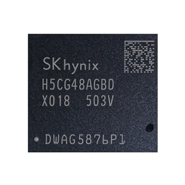
H5CG48AGBDX018 - 16Gb DDR5-5600 DRAM, 1.1V | SK hynix
MPN: H5CG48AGBDX018 ✓ Active| Qty | Unit Price | Extended |
|---|---|---|
| 1 | $109.6875 | $109.69 |
| 10 | $79.2188 | $792.19 |
| 100 | $70.0781 | $7,007.81 |
| 500 | $67.0313 | $33,515.65 |
| 1,000 | $63.9844 | $63,984.40 |
H5CG48AGBDX018 Overview
DDR5 SDRAM (Double Data Rate 5 synchronous dynamic random access memory) is the fifth generation of DDR memory standards, succeeding DDR4 with higher transfer rates, lower operating voltage, on-die ECC, and bank-group architecture improvements. In the memory hierarchy, DRAM sits as the primary volatile working memory between CPU caches and non-volatile storage such as NAND flash, making DDR5 devices core components of power management and compute subsystems in servers, PCs, and embedded modules.
Key features of the H5CG48AGBDX018 include its 16Gb density per die in a x8 organization, a 5600 Mbps data rate (DDR5-5600 speed grade, corresponding to a 2800 MHz clock), and a reduced 1.1V core supply compared with 1.2V for DDR4. DDR5 architecture splits each rank into two independent channels, improving effective bandwidth and channel efficiency. On-die ECC improves data reliability without host-side overhead, and the FBGA-82 fine-pitch ball grid array package supports high-density module assembly.
Technically, the device operates from a 1.1V VDD supply with a separate supply domain, uses bank-group structure for faster random access, and implements DDR5 timing parameters such as tCK, tRAS, and tRP per the SK hynix DDR5 datasheet. Termination and power management are handled in-system by PMICs on registered DIMMs (RDIMM) or by host power rails on soldered-down designs.
Typical applications include client and server computing modules, industrial controllers requiring high-bandwidth memory, networking equipment, and replacement sourcing for DDR5-based systems.
Design consideration: DDR5 devices require careful trace-length matching, on-die termination calibration (ZQ calibration), and verification of platform memory-controller support for the DDR5-5600 speed grade; substituting parts may require BIOS or firmware timing adjustments.
This page synthesizes distributor pricing, stock data, drop-in alternatives, and practical design notes not found in the manufacturer datasheet.
Drop-in alternatives for H5CG48AGBDX018 — same package, pin-to-pin compatible. Different-package parts requiring PCB rework are excluded.
Variants in this series
Same-series models that are drop-in compatible with H5CG48AGBDX018 (same form factor and footprint) — differing in Interface, Package, Organization, Density, Data Rate.
Quick Comparison Tool — Select alternative parts for side-by-side comparison:
H5CG48AGBDX018N
✓ In Stock
$87.42 / Unit
View Datasheet →H5CG48AGBDX014
✓ In Stock
$86 / Unit
View Datasheet →H5CGD8AGBDX018
📋 Reference alternative (not in catalog)
H5CG48AGBDX018 Maximum Ratings & Electrical Characteristics
| Memory Type | DDR5 SDRAM |
| Density | 16 Gbit |
| Organization | 2G x 8 |
| Data Rate | 5600 Mbps/pin (DDR5-5600) |
| Clock Frequency | 2800 MHz |
| Supply Voltage (VDD) | 1.1 V |
| Package | FBGA-82 |
| Mounting Type | Surface Mount |
| Interface | DDR5 (Double Data Rate 5) |
| ECC | On-die ECC (DDR5 standard feature) |
| Application Class | Computing, mobile, consumer, industrial memory |
H5CG48AGBDX018 fbga-82 Pin Configuration Guide
Pin configuration for H5CG48AGBDX018 (fbga-82 package). This digital IC includes GPIO, communication interfaces (UART, SPI, I2C), and power pins. Refer to the manufacturer datasheet for alternate pin functions and configuration options. Essential for embedded system design and PCB layout.

No detailed pinout data available for H5CG48AGBDX018.
Refer to the datasheet for full pin configuration.
Typical Applications
H5CG48AGBDX018 is suitable for 6 applications: Server and Data Center Memory Modules, Client PCs and Workstations, Industrial Controllers and Edge Computing, Networking Equipment, Test and Measurement Instrumentation, Replacement Sourcing and BOM Continuity.
Server and Data Center Memory Modules
The H5CG48AGBDX018 fits server RDIMM and soldered-down memory designs where its 16Gb density and 5600 Mbps/pin data rate maximize per-channel bandwidth. DDR5's dual 32-bit sub-channel architecture improves effective utilization, and on-die ECC raises reliability for data-center workloads. With 1.1 V operation, per-bit power drops versus DDR4, reducing thermal load in dense 1U/2U servers. On RDIMMs, an on-module PMIC supplies the 1.1 V rail, while signal integrity depends on trace matching and termination calibration per the SK hynix datasheet.
Recommended
Client PCs and Workstations
Desktop and mobile platforms with Intel or AMD DDR5 memory controllers support 5600 Mbps speed grades, making the H5CG48AGBDX018 a fit for UDIMM and SODIMM module builds. The 16Gb density enables 16 GB single-rank modules and higher-capacity configurations with fewer dies. On-die ECC improves stability for long-running client workloads without host overhead. Designers should confirm platform QVL approval and memory training compatibility, since swapping DDR5 dies can require BIOS reference-code updates; the 1.1 V supply simplifies shared-rail power designs on compact boards.
Recommended
Industrial Controllers and Edge Computing
Per the Datasheet Directory overview, the H5CG48AGBDX018N is explicitly positioned for industrial controllers and embedded logging. Its 16Gb density supports memory-hungry edge-AI inference and data buffering, while the 5600 Mbps data rate keeps DRAM from bottlenecking modern SoCs and FPGAs. Soldered-down FBGA-82 mounting avoids socket contact degradation under vibration and thermal cycling common in factory environments. Designers must verify the extended temperature range in the SK hynix datasheet and provide clean 1.1 V power with local decoupling, since industrial supplies are noisier than client platforms.
Recommended
Networking Equipment
Switches, routers, and network appliances use high-bandwidth DRAM for packet buffering, flow tables, and control-plane memory. The H5CG48AGBDX018's 5600 Mbps rate and 2Gx8 organization provide the random-access throughput needed when packet rates spike, and bank-group architecture reduces effective access latency versus flat-bank DDR4. Its 1.1 V rail lowers operating power in always-on network hardware where energy budgets matter. Layout should prioritize short, matched DQS/DQ routing and reference-plane continuity; networking boards often run DDR5 at reduced speeds to relax timing margins, which the 5600-grade die accommodates with headroom.
Recommended
Test and Measurement Instrumentation
Oscilloscopes, logic analyzers, and signal generators require deep capture memory with sustained write bandwidth. The H5CG48AGBDX018's 16Gb capacity supports long acquisition records, while the 5600 Mbps data rate sustains streaming of high-sample-rate ADC data into memory. DDR5's on-die ECC reduces silent data corruption in instruments whose measurements must be traceable and repeatable. Instruments typically run soldered-down DDR5 with conservative speed derating to guarantee operation across the full temperature range; confirm thermal and timing derating guidance in the SK hynix datasheet before locking the design.
Recommended
Replacement Sourcing and BOM Continuity
As DDR5 becomes the mainstream DRAM generation through 2026, the H5CG48AGBDX018 serves as a replacement source for DDR5-based computing modules, storage appliances, and embedded boards needing a specific density and speed grade. Multi-distributor stock (over 25,000 pcs reported across icDirectory and Octopart India as of late August 2026) supports both spot buys and scheduled orders. Buyers should verify date codes, compare the exact ordering suffix against the original BOM line, and confirm platform memory-training compatibility, since cross-reference guides warn that DDR5 substitutions may require firmware adjustments for timing parameters such as tCK, tRAS, and tRP.
Recommended
Recommended Products Summary
Engineering reference data for H5CG48AGBDX018 — comparison, design guidance, and compliance information.
Selection Guide
Comparison with Alternatives
| Parameter | This Product | H5CG48AGBDX018N | H5CGD8AGBDX018 | H5CG48AGBDX014 |
|---|---|---|---|---|
| Package | FBGA-82 | FBGA-82 - same | FBGA-82 - same | FBGA-82 - same |
| Brand | SK hynix | SK hynix | SK hynix | SK hynix |
| Density | 16 Gbit | 16 Gbit | 16 Gbit | 16 Gbit |
| Organization | 2G x 8 | 2G x 8 | 2G x 8 | 2G x 8 |
| Data Rate | 5600 Mbps/pin | 5600 Mbps/pin | 5600 Mbps/pin | 4800 Mbps/pin |
| Supply Voltage | 1.1 V | 1.1 V | 1.1 V | 1.1 V |
| Memory Type | DDR5 SDRAM | DDR5 SDRAM | DDR5 SDRAM | DDR5 SDRAM |
Key Differentiators
- Highest mainstream DDR5 speed grade (vs H5CG48AGBDX014)
- Catalog-listed availability with published pricing (vs H5CGD8AGBDX018)
- Lower per-bit power than DDR4 predecessors (vs H5ANAG6NCMR-XNC (DDR4 16Gb))
Design Notes
DDR5 at 5600 Mbps demands strict fly-by command/address routing and length-matched DQ/DQS pairs within each nibble group. Keep trace skew within the limits defined in the SK hynix datasheet, maintain solid reference planes under all high-speed nets, and avoid splitting DQ pairs across plane voids. On soldered-down designs, run full memory training during firmware bring-up; on modules, rely on the on-DIMM PMIC and register clock driver topology. Verify ZQ calibration resistor placement close to the ZQ ball with a precision 240-ohm-class reference resistor per the datasheet.
The H5CG48AGBDX018 operates from a 1.1 V core supply. Estimated: at full 5600 Mbps read/write activity a single 16Gb die draws on the order of hundreds of milliwatts; size the 1.1 V rail per the datasheet IDD/IDDQ tables for your actual utilization pattern rather than estimates. On registered DIMMs, use a DDR5-compliant on-module PMIC; on soldered-down boards, provide bulk plus high-frequency decoupling (10 uF bulk per die group plus 0.1 uF ceramics at each power ball) and sequence rails per the DDR5 power-up procedure in the datasheet.
Do not assume cross-vendor DDR5 interchangeability. DDR5 FBGA ballouts, addressing schemes, and training features are not pin-to-pin standardized across manufacturers, and timing parameters (tCK, tRAS, tRP) can differ even at the same speed grade; cross-reference guides explicitly warn that substitution may require BIOS or memory reference code changes. Also confirm the exact ordering suffix (e.g., H5CG48AGBDX018 vs H5CG48AGBDX018N) with your distributor, and verify temperature-grade markings on received date codes before production assembly.
Place the FBGA-82 die to minimize overall flight-time skew across the channel. Use via-in-pad or short dog-bone escapes to keep stubs under a few mils at 5600 Mbps. Estimated: at 2800 MHz fundamental clock, even a 1 mm unterminated stub is electrically significant, so back-drill or blind via techniques may be needed on thick server boards. Follow the PCB routing topology (write leveling, read training nodes) shown in the SK hynix DDR5 design guide and platform vendor reference layouts.
Compliance Information
Compliance data not present in verified web data; confirm RoHS/REACH status on the SK hynix product page or datasheet before procurement.