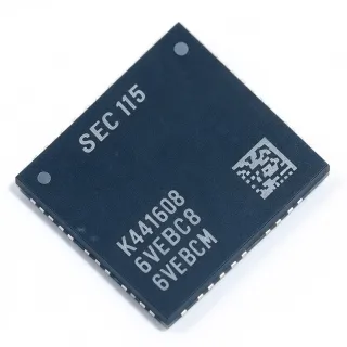
H5CG48AGBDX014 - 16Gb DDR5 SDRAM 4800Mbps | SK hynix | Server Memory
MPN: H5CG48AGBDX014 ✓ Active| Qty | Unit Price | Extended |
|---|---|---|
| 1 | $92.5 | $92.50 |
| 10 | $90.1 | $901.00 |
| 100 | $88.4 | $8,840.00 |
| 500 | $87.42 | $43,710.00 |
| 1,000 | $86 | $86,000.00 |
H5CG48AGBDX014 Overview
DDR5 SDRAM is the fifth generation of double-data-rate synchronous DRAM, the memory technology at the base of the DRAM -> memory IC -> semiconductor hierarchy. Compared with DDR4, DDR5 improves speed, density, and power efficiency, and standardizes on-die ECC so that server-class data reliability can be maintained even in mainstream form factors. The JEDEC-standard DDR5 interface moves to two independent 32-bit sub-channels per DIMM, improving effective bandwidth and channel utilization.
The H5CG48AGBDX014 delivers 16Gb of density in a single x8 component, enabling high-capacity UDIMM, RDIMM, and soldered-down memory solutions. Its 1.1V VDD reduces per-bit energy versus 1.2V DDR4, while the 4800 Mbps speed grade supports mainstream server and desktop platforms. On-die ECC detects and corrects single-bit internal DRAM errors, reducing system-level soft-error exposure.
According to the SK hynix DDR5 e-Catalogue, SK hynix shipped the world's first DDR5 in a server solution, positioning this family for AI, big data, and cloud workloads. Typical applications include server main memory modules, high-performance desktops, embedded computing, networking appliances, and industrial systems migrating from DDR4.
Designers should note that DDR5 components require PMIC-managed power rails (on-module for DIMMs), on-die termination (ODT), and decision-feedback equalization (DFE) support at the memory controller, so BIOS/MRC and controller training sequences must be validated for the exact component speed bin.
This page adds value beyond the datasheet by consolidating drop-in cross-reference candidates, distributor pricing context, and sourcing guidance for the allocation-constrained DDR5 component market.
Drop-in alternatives for H5CG48AGBDX014 — same package, pin-to-pin compatible. Different-package parts requiring PCB rework are excluded.
Variants in this series
Same-series models that are drop-in compatible with H5CG48AGBDX014 (same form factor and footprint) — differing in Package, Density, Interface, Data Rate, RoHS Status.
Quick Comparison Tool — Select alternative parts for side-by-side comparison:
H5CG48AGBDX018N
✅ Drop-In✓ In Stock
$87.42 / Unit
View Datasheet →H5CG48AGBDX018
✅ Drop-In✓ In Stock
$63.9844 / Unit
View Datasheet →H5CG48MEBDX014N
✅ Drop-In✓ In Stock
$41.68 / Unit
View Datasheet →H5CG48MEBDX018N
✅ Drop-In✓ In Stock
$1 / Unit
View Datasheet →H5CG48AGBDX014 Maximum Ratings & Electrical Characteristics
| Manufacturer | SK hynix |
| Product Type | DDR5 SDRAM Component |
| Density | 16Gb (2Gx8) |
| Organization | 2G x 8 |
| Data Rate | 4800 Mbps |
| Supply Voltage (VDD) | 1.1 V |
| Error Correction | On-die ECC (ODECC) |
| Package | 82-ball FBGA |
| Interface Type | DDR5 (double data rate, 5th generation) |
| Application Segment | Server, mainstream PC, industrial |
| Configuration Target | UDIMM / RDIMM / soldered-down |
| Termination | On-die termination (ODT) |
| Mounting Type | Surface Mount |
H5CG48AGBDX014 82-ball fbga Pin Configuration Guide
Pin configuration for H5CG48AGBDX014 (82-ball fbga package). This digital IC includes GPIO, communication interfaces (UART, SPI, I2C), and power pins. Refer to the manufacturer datasheet for alternate pin functions and configuration options. Essential for embedded system design and PCB layout.

No detailed pinout data available for H5CG48AGBDX014.
Refer to the datasheet for full pin configuration.
Typical Applications
H5CG48AGBDX014 is suitable for 6 applications: Server Main Memory (RDIMM), High-Performance Desktop UDIMM, AI and Big Data Compute Nodes, Networking Appliances, Industrial Embedded Computing, Test and Measurement Systems.
Server Main Memory (RDIMM)
The H5CG48AGBDX014 fits server main memory modules where per-bit power and error resilience dominate the design. Its 16Gb 2Gx8 organization lets one RDIMM rank reach 32GB with sixteen components, while DDR5-4800 at 1.1V cuts memory power versus comparable DDR4-3200 solutions. On-die ECC corrects internal single-bit errors, complementing RDIMM side-band ECC for full server reliability coverage. In the module, the component's 4800 Mbps bus connects through the registered clock driver and data buffers; the trade-off versus faster bins is lower peak bandwidth but better channel-margin and lower cost at scale. SK hynix positioned its DDR5 family for the AI and big-data era with the world's first DDR5 server solution.
Recommended
High-Performance Desktop UDIMM
For enthusiast and workstation desktops, the H5CG48AGBDX014 provides 16Gb per component, enabling 32GB single-rank UDIMMs with only sixteen chips and clean signal routing. The 2Gx8 organization with DDR5-4800 matches the JEDEC default speed support of mainstream desktop CPU memory controllers, guaranteeing out-of-the-box compatibility without overclocking profiles. Its 1.1V supply and ODECC reduce thermal load inside cramped desktop chassis, improving long-term retention reliability. In a UDIMM, the components connect directly to the 288-pin DDR5 edge connector; unlike RDIMMs there is no register, so trace-length matching and ODT settings from the memory controller directly govern achievable bus speed. Higher 5600 bins can be substituted where the platform supports them.
Recommended
AI and Big Data Compute Nodes
SK hynix introduced its DDR5 family explicitly to enable the era of AI and big data, and the H5CG48AGBDX014 contributes the memory capacity those workloads demand. Dense 16Gb components let 2U servers carry terabytes of main memory for in-memory analytics, model training data staging, and caching tiers between HBM/accelerator memory and storage. The DDR5 two-sub-channel architecture raises effective bandwidth utilization for the bursty access patterns typical of data pipelines, while 4800 Mbps per pin at 1.1V balances throughput against the aggressive power budgets of dense compute racks. On-die ECC keeps silent data corruption risk low across the large component counts such systems require.
Recommended
Networking Appliances
Routers, switches, and security gateways need large packet buffers and flow tables that exceed what SRAM or embedded memory can economically provide. The H5CG48AGBDX014 supplies 16Gb of DDR5 per component with 4800 Mbps bandwidth, supporting line-rate processing in aggregation platforms while its 1.1V operation eases thermal design in fanless or constrained enclosures. In soldered-down configurations, two components provide 4GB of buffering directly on the control card, and the FBGA footprint keeps routing short between the network processor and memory. On-die ECC protects against soft errors during long-duty-cycle operation, an important consideration for telecom infrastructure targeting high availability service levels.
Recommended
Industrial Embedded Computing
Industrial PCs, machine-vision controllers, and edge AI gateways migrating from DDR4 to DDR5 platforms use the H5CG48AGBDX014 for main memory. Its 16Gb density allows compact COM Express or SMARC carrier designs to reach 8-16GB with only four to eight components soldered directly on the module, improving vibration tolerance versus SO-DIMM sockets. DDR5-4800 at 1.1V delivers the bandwidth needed for multi-camera vision pipelines and local inference while lowering memory-rail power in passively cooled enclosures. Designers must confirm the component temperature grade matches the industrial ambient range and validate DDR5 controller training across the full temperature span, since training margins differ from DDR4 platforms.
Recommended
Test and Measurement Systems
High-speed oscilloscopes, logic analyzers, and protocol testers require deep capture memory to retain long acquisitions at full sample rate. The H5CG48AGBDX014 provides 16Gb per component at DDR5-4800, giving instrument designers substantially more streaming depth per chip than DDR4-class parts, with on-die ECC safeguarding measurement record integrity during extended thermal soak. Banks of these components, organized across 64-bit or 128-bit buses, feed acquisition ASICs and FPGAs; the 82-ball FBGA supports the dense multichip layouts typical of acquisition memory boards. Because instrument platforms have long service lives, qualifying both the A-die and M-die (H5CG48MEBDX014N) variants protects against future allocation gaps.
Recommended
Recommended Products Summary
Engineering reference data for H5CG48AGBDX014 — comparison, design guidance, and compliance information.
Selection Guide
Comparison with Alternatives
| Parameter | This Product | H5CG48AGBDX018N | H5CG48MEBDX014N | H5CG48MEBDX018N |
|---|---|---|---|---|
| Brand | SK hynix | SK hynix | SK hynix | SK hynix |
| Package | 82-ball FBGA | 82-ball FBGA - same | 82-ball FBGA - same | 82-ball FBGA - same |
| Density | 16Gb | 16Gb | 16Gb | 16Gb |
| Organization | 2G x 8 | 2G x 8 | 2G x 8 | 2G x 8 |
| Data Rate | 4800 Mbps | 5600 Mbps | 4800 Mbps | 5600 Mbps |
| Supply Voltage | 1.1 V | 1.1 V | 1.1 V | 1.1 V |
| On-die ECC | Yes (ODECC) | Yes (ODECC) | Yes (ODECC) | Yes (ODECC) |
| Die Generation | A-die | A-die | M-die (newer process) | M-die (newer process) |
| Primary Segments | Server, mainstream PC, industrial | Server, PC, industrial | Server, PC, industrial | Server, PC, industrial |
Key Differentiators
- Lower platform power at DDR5 standard voltage (vs H5ANAG6NCMR-XNI (DDR4))
- Cost-effective entry speed bin (vs H5CG48AGBDX018N)
- A-die channel stock availability (vs H5CG48MEBDX014N)
Design Notes
DDR5-4800 operation requires careful fly-by command/address routing with per-byte data-mask (DBI) and DQS differential pairs length-matched within tight tolerances. On UDIMM and soldered-down designs, follow the SK hynix DDR5 device operation documentation for ODT and write-levelization settings. The DDR5 DFE (decision feedback equalization) on the DRAM side must be enabled and trained by the controller - do not assume DDR4 training routines port over; budget firmware bring-up time for DDR5 memory-training validation across process, voltage, and temperature corners.
The H5CG48AGBDX014 runs on the DDR5-standard 1.1V VDD rail, but DDR5 systems also require VDDQ (1.1V) and VPP (1.8V) rails. On DIMM designs, DDR5 moves the PMIC onto the module itself, so select a module PMIC rated for the total load of sixteen 16Gb components. On soldered-down boards, provide clean 1.1V rails with bulk and high-frequency decoupling close to each component, and verify rail sequencing per the DDR5 specification before releasing power-tree design.
The '014' suffix in the MPN encodes the 4800 Mbps speed bin - substituting an 018N (5600) part is footprint-compatible but changes SPD content and controller training targets, while substituting a slower bin is not possible. Also verify die revision (A-die vs M-die) acceptance in platform qualified-vendor lists, since some server BIOS/MRC releases whitelist specific die revisions. Obtain the official SK hynix part number decoder from the downloads portal to decode the full ordering code including temperature grade before committing a BOM.
Compliance Information
Compliance data not present in the provided verified web data; consult the official SK hynix datasheet and product compliance documentation.