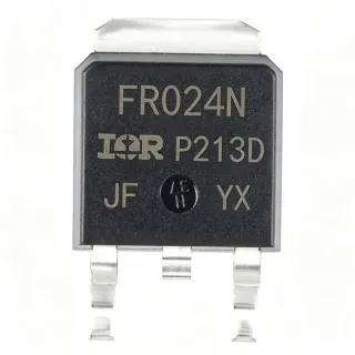
IRLR7843TRPBF - 30V 161A N-Ch HEXFET MOSFET | Infineon
MPN: IRLR7843TRPBF ✓ Active| Qty | Unit Price | Extended |
|---|---|---|
| 1 | $0.97 | $0.97 |
| 10 | $0.84 | $8.40 |
| 100 | $0.72 | $72.00 |
| 500 | $0.61 | $305.00 |
| 1,000 | $0.54 | $540.00 |
| 2,500 | $0.48 | $1,200.00 |
IRLR7843TRPBF Overview
A power MOSFET (Metal-Oxide-Semiconductor Field-Effect Transistor) is a voltage-controlled switch used for power conversion and switching applications. As a member of the discrete semiconductor hierarchy, MOSFETs sit beneath the broader category of transistors and are the workhorse of modern switch-mode power supplies (SMPS), motor drives, and load switches. N-channel enhancement-mode MOSFETs like the IRLR7843TRPBF are the dominant topology for low-voltage, high-current rails because their lower on-resistance per unit silicon area minimizes conduction loss.
Key differentiating features include a logic-level-compatible gate drive, fully characterized avalanche energy and current, and an ultra-low gate impedance that supports fast switching edges. The TO-252AA (DPAK) surface-mount package delivers a low thermal resistance path when soldered to a copper pad area of approximately 1 square inch, making it suitable for both hand-soldered prototypes and high-volume SMT assembly lines.
Architecturally, the IRLR7843TRPBF uses a planar HEXFET cell structure with a vertical current flow that maximizes die area utilization. The combination of 30V drain-source breakdown voltage, sub-4 mOhm Rds(on), and 34 nC gate charge makes it well-balanced for synchronous rectification in 12V-input buck converters and for OR-ing/low-side switch roles in telecom and industrial power systems.
Typical applications include high-frequency synchronous buck converters for computer processor power, isolated DC-DC converters with synchronous rectification for telecom and industrial use, and OR-ing/low-side switches in multi-rail systems. The part is lead-free (Pb-free suffix) and RoHS compliant per Infineon's product page.
When designing with this device, prioritize gate-drive strength - a 1A peak gate driver is recommended for fast turn-on/off, and the source connection should be Kelvin-connected to the gate driver return to avoid source-inductance-induced turn-off transients. Estimate junction temperature under worst-case conduction and switching conditions before finalizing PCB copper area.
This page synthesizes distributor pricing, drop-in alternatives, and practical design notes not found in the manufacturer datasheet.
Drop-in alternatives for IRLR7843TRPBF — same package, pin-to-pin compatible. Different-package parts requiring PCB rework are excluded.
Variants in this series
Same-series models that are drop-in compatible with IRLR7843TRPBF (same form factor and footprint) — differing in Technology, Package, Operating Temperature Range, FET Type, On-Resistance RDS(on) max @ VGS=10V.
Quick Comparison Tool — Select alternative parts for side-by-side comparison:
IRLR3636TRPBF
✅ Drop-In✓ In Stock
$2.38 / Unit
View Datasheet →IRLR2905TRPBF
✅ Drop-In✓ In Stock
$0.61 / Unit
View Datasheet →IRLR3114ZTRPBF
✅ Drop-In✓ In Stock
$0.46 / Unit
View Datasheet →BSC050NE2LSATMA1
✅ Drop-In✓ In Stock
$0.36 / Unit
View Datasheet →BSC016N06NSATMA1
✅ Drop-In✓ In Stock
$0.65 / Unit
View Datasheet →VBE1303
✅ Drop-In📋 Reference alternative (not in catalog)
IRLR7843TRPBF Maximum Ratings & Electrical Characteristics
| Polarity | N-Channel |
| Drain-Source Voltage (Vdss) | 30 V |
| Continuous Drain Current (Id) @ Tc=25C | 161 A |
| Power Dissipation (Pd) @ Tc=25C | 140 W |
| On-Resistance Rds(on) Max @ Vgs=10V | 3.3 mOhm |
| On-Resistance Rds(on) Max @ Vgs=4.5V | 4.5 mOhm (typ) |
| Total Gate Charge (Qg) | 34 nC |
| Gate-to-Source Voltage Max | ±20 V |
| Avalanche Energy (Eas) | Fully characterized |
| Operating Temperature Range | -55C to +175C |
| Package | TO-252AA (DPAK) |
| Mounting Type | Surface Mount |
| Technology | HEXFET |
| Lead-Free / RoHS | Yes (PBF suffix = lead-free) |
IRLR7843TRPBF Pin Configuration
| Pin 1 | Gate — Gate drive input; connect to gate-driver output |
| Pin 2 | Drain — Drain terminal; electrically continuous with the mounting tab |
| Pin 3 | Source — Source terminal; reference for gate drive |
| Pin TAB | Drain (Tab) — Mounting tab - electrically tied to pin 2 (Drain); primary thermal path |
Safe Operating Area - IRLR7843TRPBF
Typical Applications
IRLR7843TRPBF is suitable for 6 applications: 12V Synchronous Buck Converter for Processor Power, Isolated DC-DC Converter with Synchronous Rectification, Battery Protection and OR-ing Switch (12V Systems), Motor Drive H-Bridge (Low-Side Position), Hot-Swap / Load Switch Controller, LED Driver High-Side Switch.
12V Synchronous Buck Converter for Processor Power
The IRLR7843TRPBF is well-matched to the low-side synchronous FET position in a 12V-input, multi-phase buck converter for server or workstation processor VRMs. Its 30V Vdss rating provides 18V of headroom above a 12V bus with margin for transients, while the 3.3 mOhm Rds(on) at Vgs=10V keeps conduction loss below 3W at 30A per phase. The 34 nC total gate charge supports 500 kHz+ switching frequencies when paired with a 1A peak gate driver, reducing output inductor size. Designers should verify avalanche energy and thermal resistance under hard-switching conditions during worst-case load transients.
Recommended
Isolated DC-DC Converter with Synchronous Rectification
The IRLR7843TRPBF functions as a self-driven or controller-driven synchronous rectifier on the secondary side of telecom and industrial isolated DC-DC converters. Its ultra-low 3.3 mOhm Rds(on) directly improves rectifier efficiency by replacing Schottky diode forward-voltage drops (typically 0.4-0.5V) with milliohm-level resistive drops. Per Infineon's datasheet, the device's fully characterized avalanche rating provides robustness during transformer reset transients common in forward and active-clamp topologies. Use a digital isolator or pulse transformer for gate drive synchronization with the primary-side controller.
Recommended
Battery Protection and OR-ing Switch (12V Systems)
The IRLR7843TRPBF serves as a low-side OR-ing switch or reverse-battery protection MOSFET in 12V battery-backed systems such as UPS modules, e-bike controllers, and industrial telemetry. Its 161A continuous rating handles inrush currents during battery paralleling, and the 3.3 mOhm Rds(on) limits continuous conduction loss to ~5W at 40A. The ±20V Vgs rating provides ample margin against gate-drive transients. Designers should use a dedicated gate driver IC rather than pulling the gate high directly from the battery rail to ensure controlled turn-on/off and avoid body-diode shoot-through.
Recommended
Motor Drive H-Bridge (Low-Side Position)
The IRLR7843TRPBF occupies the low-side positions of a brushed DC or PMSM H-bridge motor driver where its 30V Vdss and 161A rating handle the inductive kickback from 12-24V motors. The ultra-low gate impedance enables fast switching edges, reducing switching losses at 20-50 kHz PWM frequencies typical of small motor drives. For higher-voltage motor systems, consider the IRLR3114ZTRPBF (40V) or BSC016N06NSATMA1 (60V) drop-in alternatives. Always add flyback diodes or use the body diode's avalanche rating to manage inductive energy during PWM commutation.
Recommended
Hot-Swap / Load Switch Controller
The IRLR7843TRPBF functions as the main pass element in a -48V telecom or 12V distributed-architecture hot-swap controller, leveraging its 161A inrush capability to charge bulk output capacitors during board insertion. The TO-252AA DPAK package dissipates initial inrush losses effectively when soldered to adequate copper. A dedicated hot-swap controller IC (e.g., current-limited gate driver) is recommended to manage inrush dV/dt and provide fault isolation. Verify SOA during the inrush transient using the datasheet's pulsed-current curves.
Recommended
LED Driver High-Side Switch
The IRLR7843TRPBF operates as a high-side PWM switch for high-brightness LED strings in automotive, architectural, and stage-lighting applications. Its fast switching capability supports PWM dimming frequencies above 1 kHz without visible flicker, while the 3.3 mOhm Rds(on) limits steady-state conduction loss. The 30V Vdss rating suits 12V-24V LED bus architectures. For high-side switching, ensure the gate driver provides a voltage reference above the LED string's top rail - a bootstrap or charge-pump driver is typically required.
Recommended
Recommended Products Summary
Engineering reference data for IRLR7843TRPBF — comparison, design guidance, and compliance information.
Selection Guide
Comparison with Alternatives
| Parameter | This Product | IRLR3636TRPBF | IRLR2905TRPBF | IRLR3114ZTRPBF | BSC050NE2LSATMA1 | BSC016N06NSATMA1 | VBE1303 |
|---|---|---|---|---|---|---|---|
| Brand | Infineon | Infineon | Infineon | Infineon | Infineon | Infineon | VBsemi |
| Package | TO-252AA (DPAK) | TO-252AA (DPAK) - same | TO-252AA (DPAK) - same | TO-252AA (DPAK) - same | TO-252AA (DPAK) - same | TO-252AA (DPAK) - same | TO-252AA (DPAK) - same |
| Drain-Source Voltage (Vdss) | 30 V | 30 V | 55 V | 40 V | 25 V | 60 V | 30 V |
| Technology | HEXFET | HEXFET | HEXFET | HEXFET | OptiMOS | OptiMOS | Trench MOSFET |
| Lead-Free / RoHS | Yes (PBF) | Yes (PBF) | Yes (PBF) | Yes (PBF) | Yes | Yes | Yes |
Key Differentiators
- Ultra-low 3.3 mOhm Rds(on) in DPAK package for 30V-class designs (vs IRLR2905TRPBF)
- Lower Rds(on) than earlier-generation 30V HEXFETs (vs BSC050NE2LSATMA1)
- Established HEXFET technology base with broad second-source availability (vs VBE1303)
Design Notes
Estimated: at 30A continuous load with Rds(on)=3.3 mOhm, conduction loss is approximately P=I²R = 30² × 0.0033 = ~3W. With a TO-252AA junction-to-ambient thermal resistance of ~50C/W on a 1 sq inch copper pad, junction temperature rise is ~150C above ambient - exceeding safe limits. For continuous operation above 15A, a larger copper area (4+ sq inches), forced airflow, or a D2PAK-packaged part (IRFS4321TRLPBF family) is required. Always cross-check with the datasheet's thermal derating curves and measure Tj under worst-case load.
Use a Kelvin-source connection when driving the gate - return the gate-driver ground to the source pin directly, not via the power ground plane, to avoid source-inductance-induced turn-off transients that can overstress Vgs. Keep the gate-drive loop area minimal (<1 sq cm) and route gate traces away from drain switching nodes. Place input bypass capacitors (1uF X7R) directly at the drain pin when used in buck topologies. The DPAK tab must be soldered to a continuous copper pour to meet the 140W dissipation rating.
Do not exceed ±20V on the gate - the thin gate oxide is vulnerable to overvoltage. Use a gate-source Zener clamp (15V) when inductive transients are possible. For synchronous rectification, add sufficient dead-time (typically 30-100 ns) to prevent body-diode shoot-through during controller transitions. The 30V Vdss rating is absolute maximum - derate to 80% (24V) for reliable continuous operation per industry best practice.
The TO-252AA (DPAK) package requires a minimum land pattern per IPC-7351: drain pad ~6.5mm × 7.4mm, gate and source pads ~1.0mm × 1.0mm. Stencil aperture for the drain pad should be 1:1 to maximize solder joint thermal conductivity. For lead-free reflow (SAC305), follow JEDEC J-STD-020 profile with peak temperature 245-260C. Avoid placing thermal reliefs on the drain pad - they significantly increase thermal resistance.
Compliance Information
PBF suffix indicates lead-free, RoHS-compliant construction per Infineon product page. AEC-Q100 status not specified in retrieved web data - assume not qualified for automotive unless explicitly verified. REACH compliance is implied by EU distribution via DigiKey/Mouser but not separately certified in retrieved data.