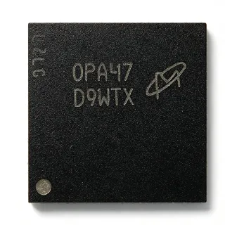
MT42L32M32D1HE-18 - 1Gbit LPDDR2 SDRAM 533MHz | Micron
MPN: MT42L32M32D1HE-18 IT:D ✓ Active| Qty | Unit Price | Extended |
|---|---|---|
| 1 | $0 | $0.00 |
| 10 | $0 | $0.00 |
| 100 | $0 | $0.00 |
| 500 | $0 | $0.00 |
| 1,000 | $0 | $0.00 |
MT42L32M32D1HE-18 IT:D Overview
LPDDR2 (Low Power Double Data Rate 2) is a JEDEC-standard SDRAM family derived from mobile DDR memory, optimized for low power consumption and high density in battery-powered and thermally constrained systems. Within the memory hierarchy, LPDDR2 sits between classic LPDDR1 and LPDDR3, introducing a 1.2V core voltage and CA (command/address) pin multiplexing that reduces pin count and simplifies PCB routing.
Key features of this device include the 1Gbit density in a single x32 organization, 533 MHz data rate operation (LPDDR2-1066 class), the compact 134-VFBGA (10 x 11.5 mm) footprint, and an industrial operating temperature range appropriate for the IT grade suffix. The D suffix in the ordering code indicates lead-free, RoHS-compliant manufacturing.
From an architectural standpoint, the device implements LPDDR2-S4 (standard DRAM) protocol with multiplexed command/address inputs, programmable burst lengths, and multiple low-power modes including deep power-down, self-refresh, and partial-array self-refresh, allowing system designers to trade standby current against wake-up latency. Bank interleaving sustains effective bandwidth close to the theoretical peak during real workloads.
Typical applications include industrial controllers requiring high-speed working memory, embedded computing modules, automotive infotainment platforms (using the AAT automotive variant), networking equipment buffers, and test and measurement instrumentation. The x32 bus width provides wide, low-latency access well suited to processors without memory controllers optimized for narrow x16 DRAM.
A key design consideration is signal integrity at 533 MHz: match CA and DQ trace lengths within the processor memory controller guidelines, and follow the VFBGA ball-map fan-out recommendations in the Micron datasheet. Power delivery must support simultaneous switching currents with adequate bulk and ceramic decoupling on both VDD1 (1.2V) and VDD2 rails.
This page synthesizes distributor pricing tiers, drop-in alternatives, comparison tables, and practical design notes not found in the manufacturer datasheet, providing engineers with sourcing and design context in a single reference.
Drop-in alternatives for MT42L32M32D1HE-18 IT:D — same package, pin-to-pin compatible. Different-package parts requiring PCB rework are excluded.
Variants in this series
Same-series models that are drop-in compatible with MT42L32M32D1HE-18 IT:D (same form factor and footprint) — differing in Interface, Organization, RoHS Status.
Quick Comparison Tool — Select alternative parts for side-by-side comparison:
MT42L32M32D1HE-18 AAT:D
✅ Drop-In📋 Reference alternative (not in catalog)
MT42L32M32D1HE-18 IT:D TR
✅ Drop-In📋 Reference alternative (not in catalog)
MT42L32M32D1HE-18 IT
✅ Drop-In📋 Reference alternative (not in catalog)
MT42L32M32D1HE-18 AIT
✅ Drop-In📋 Reference alternative (not in catalog)
MT42L16M32D1HE-18
✅ Drop-In ⚠️ Specs Unverified✓ In Stock
$2.9 / Unit
View Datasheet →MT42L32M32D1HE-18 IT:D Maximum Ratings & Electrical Characteristics
| Memory Type | Mobile LPDDR2 SDRAM |
| Memory Size | 1 Gbit |
| Organization | 32M x 32 |
| Interface | Parallel |
| Clock / Data Rate | 533 MHz |
| Core Supply Voltage (VDD1) | 1.2 V |
| I/O Supply Voltage (VDD2) | 1.8 V |
| Package | 134-VFBGA (10 x 11.5 mm) |
| Mounting Type | Surface Mount |
| Temperature Grade | IT (industrial) |
| RoHS Status | Compliant (D suffix = lead-free) |
| AEC-Q100 | Qualified on AAT automotive variants |
| Access Type | Synchronous, JEDEC LPDDR2-S4 protocol |
| Refresh | Self-refresh supported |
| Packaging Option | Tray or Tape & Reel (TR) |
MT42L32M32D1HE-18 IT:D 134-vfbga (10 x 11.5 mm) Pin Configuration Guide
Pin configuration for MT42L32M32D1HE-18 IT:D (134-vfbga (10 x 11.5 mm) package). This digital IC includes GPIO, communication interfaces (UART, SPI, I2C), and power pins. Refer to the manufacturer datasheet for alternate pin functions and configuration options. Essential for embedded system design and PCB layout.

No detailed pinout data available for MT42L32M32D1HE-18 IT:D.
Refer to the datasheet for full pin configuration.
Typical Applications
MT42L32M32D1HE-18 IT:D is suitable for 6 applications: Industrial Controllers and Automation, Embedded Computing Modules (SoM), Automotive Infotainment and Telematics, Networking and Communications Equipment, Medical and Diagnostic Instrumentation, Test and Measurement Instruments.
Industrial Controllers and Automation
Industrial PLCs and motion controllers need working memory that survives wide ambient swings and vibration-tolerant SMD assembly, making the IT-grade MT42L32M32D1HE-18 a strong fit. Its 1 Gbit capacity in a single x32-wide device simplifies the memory subsystem: one 32-bit data bus and one 134-VFBGA footprint replace multi-chip x16 configurations, reducing trace count and BOM complexity. At 533 MHz the device supplies roughly 2 GB/s peak bandwidth over a 32-bit bus, sufficient for real-time control loops, HMI buffering, and fieldbus stacks. Self-refresh and deep power-down modes let the controller retain state through operator-initiated shutdowns while keeping standby current low, which matters in enclosed cabinets with limited thermal budget.
Recommended
Embedded Computing Modules (SoM)
System-on-module vendors building ARM-based compute modules frequently specify LPDDR2 for its 1.2V core voltage and multiplexed command/address bus, which shortens trace lengths inside dense module stacks. The MT42L32M32D1HE-18's 32M x 32 organization pairs naturally with SoC memory controllers wired for a single 32-bit LPDDR2 port, sustaining up to 533 MHz DDR transfers. Because the memory sits on the module, the 10 x 11.5 mm VFBGA keeps height low enough for heat spreaders and connectors. Designers should follow the Micron layout guidelines for length-matched CA and DQS strobes; on a 6-8 layer module stackup, controlled-impedance routing typically holds skew within controller spec while the D suffix guarantees RoHS-compliant reflow profiles.
Recommended
Automotive Infotainment and Telematics
For automotive head units, cluster displays, and telematics gateways, the AAT:D variant of this same die carries AEC-Q100 qualification, allowing one PCB design to serve both industrial and automotive builds. Infotainment workloads - navigation tile rendering, media buffering, voice processing - fit comfortably within the 1 Gbit density and 533 MHz data rate of a 32-bit LPDDR2 port, and legacy SoCs (for example, earlier-generation automotive applications processors) implement LPDDR2 controllers natively. The automotive variant's extended temperature rating covers cabin and near-engine mounting zones. Designers should add margin in the power tree for crank-pulse transients and verify self-refresh retention across ignition-off sleep states, where deep power-down minimizes quiescent drain on the battery during parking periods.
Recommended
Networking and Communications Equipment
Edge routers, industrial switches, and wireless access points use packet-buffer memory where wide buses reduce latency: the x32 organization of the MT42L32M32D1HE-18 delivers twice the words per burst compared with x16 parts, sustaining line-rate forwarding for 100M/1G ports at 533 MHz. Bank interleaving across the LPDDR2-S4 address map hides row-activation latency during scattered packet reads and writes, and partial-array self-refresh lets management-traffic buffers stay resident while bulk queues power down overnight in energy-aware deployments. The 1.2V core keeps memory power a small share of a fanless switch budget. Thermal design is straightforward: dissipation at VDD1 = 1.2 V remains low enough that a ground-plane heat spreader under the 134-VFBGA suffices in sealed enclosures.
Recommended
Medical and Diagnostic Instrumentation
Benchtop analyzers, portable ultrasound front ends, and patient-monitoring gateways generate image and waveform buffers that exceed internal SRAM by orders of magnitude, so a 1 Gbit LPDDR2 such as the MT42L32M32D1HE-18 provides the working memory behind acquisition ASICs. The 32-bit bus moves high-rate ADC sample streams to the processor without saturating the interface, while self-refresh preserves buffer contents through low-power standby between measurements - an important regulatory and usability feature for battery-operated point-of-care devices. The industrial temperature grade suits typical clinical environments, and the D-suffix RoHS construction aligns with medical-equipment environmental directives. Designers should validate memory error behavior under EMI test per IEC 60601 conducted/radiated immunity sections and add CRC in software for critical buffers.
Recommended
Test and Measurement Instruments
Oscilloscope front ends, logic analyzers, and signal generators need deep, fast capture memory: a single MT42L32M32D1HE-18 provides 128 MByte-class buffering per channel group at up to 533 MHz DDR, letting acquisition logic stream samples continuously while the display processor reads out asynchronously. The x32 width matches the 32-bit acquisition buses common in mid-range instruments, avoiding multi-chip interleaving logic. Deep power-down supports instrument standby modes mandated by energy regulations, and the 1.2V core keeps internal temperature rise negligible in convection-cooled enclosures. Bench instruments benefit from the IT industrial temperature rating for calibration-lab environments that lack strict climate control. For higher capture depths, two devices can share one controller with chip-select banking using the same footprint routing pattern.
Recommended
Recommended Products Summary
Engineering reference data for MT42L32M32D1HE-18 IT:D — comparison, design guidance, and compliance information.
Selection Guide
Comparison with Alternatives
| Parameter | This Product | MT42L32M32D1HE-18 AAT:D | MT42L32M32D1HE-18 IT:D TR | MT42L32M32D1HE-18 IT | MT42L16M32D1HE-18 |
|---|---|---|---|---|---|
| Package | 134-VFBGA (10 x 11.5 mm) | 134-VFBGA (10 x 11.5 mm) - same | 134-VFBGA (10 x 11.5 mm) - same | 134-VFBGA (10 x 11.5 mm) - same | 134-VFBGA (10 x 11.5 mm) - same |
| Brand | Micron Technology | Micron Technology | Micron Technology | Micron Technology | Micron Technology |
| Memory Size | 1 Gbit | 1 Gbit | 1 Gbit | 1 Gbit | 512 Mbit |
| Organization | 32M x 32 | 32M x 32 | 32M x 32 | 32M x 32 | 16M x 32 |
| Data Rate | 533 MHz | 533 MHz | 533 MHz | 533 MHz | 533 MHz |
| Supply Voltage | 1.2 V (VDD1) / 1.8 V (VDD2) | 1.2 V / 1.8 V | 1.2 V / 1.8 V | 1.2 V / 1.8 V | 1.2 V / 1.8 V |
Key Differentiators
- Automotive-qualified sibling available without redesign (vs MT42L32M32D1HE-18 IT:D (this IT:D vs AAT:D))
- Full 1 Gbit density in a single x32 device (vs MT42L16M32D1HE-18)
- Tape-and-reel option for high-volume SMT (vs MT42L32M32D1HE-18 IT:D (tray))
- Low 1.2 V core operation (vs MT41K128M16JT-125 AUT:K (DDR3L))
Design Notes
At 533 MHz DDR (1066 MT/s), trace-length matching between the LPDDR2 controller and the 134-VFBGA is critical. Keep command/address (CA) lines length-matched within the SoC memory controller's spec (typically within a few hundred mils of each other), and route each DQS strobe with its associated DQ byte. Use the ball-map fan-out in the Micron datasheet to plan inner-layer escape routing; on 8-layer module stackups, dedicate one ground plane adjacent to the memory layers for a clean return path. Avoid routing CA lines across plane splits.
The device uses a split supply: VDD1 = 1.2 V core and VDD2 = 1.8 V I/O (per distributor listings: 1.2V/1.8V). Provide separate bulk capacitance (tens of uF) plus local 0.1 uF ceramics at the VFBGA power balls, sized to handle simultaneous-switching output currents during full-burst writes. During deep power-down the core current drops to microamp levels, so design the 1.2 V rail regulator for low quiescent current if the system spends long periods in standby.
Ordering-code suffixes matter: IT:D (industrial, lead-free D), AAT:D (automotive AEC-Q100), and the legacy non-D -IT part listed on Micron's legacy page are not interchangeable for compliance documentation even though the die is the same. Verify the exact suffix on incoming reels against your BOM, especially for automotive builds that require AAT:D and PPAP. The MT42L16M32D1HE-18 (512 Mbit) fits the same footprint but halves capacity - firmware and memory maps must be re-validated before any density downgrade.
The 134-VFBGA (10 x 11.5 mm) requires via-in-pad or dog-bone fan-out with ~0.5 mm ball pitch per standard VFBGA assembly practice. Follow IPC/JEDEC reflow profiles compatible with the D-suffix lead-free construction (SnAgCu balls, peak reflow typically ~245-250 C). Place the device close to the processor to keep flight times short, and reserve board area under the BGA as a solid ground region to aid thermal dissipation and EMI containment.
Compliance Information
The :D suffix indicates the lead-free, RoHS-compliant construction per DigiKey/Micron listings. AEC-Q100 applies to the AAT:D automotive variant (per Ampheo listing), not to this IT:D part. REACH, halogen-free, and conflict-minerals status not stated in provided data.