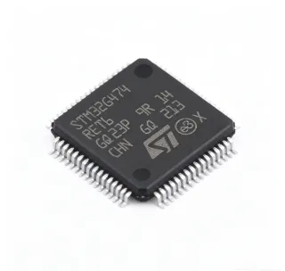
STM32G473RET6 - 170MHz ARM Cortex-M4F MCU with FPU | STMicroelectronics
MPN: STM32G473RET6 ✓ Active| Qty | Unit Price | Extended |
|---|---|---|
| 1 | $8.5 | $8.50 |
| 10 | $7.65 | $76.50 |
| 100 | $6.8 | $680.00 |
| 500 | $6.12 | $3,060.00 |
| 1,000 | $5.44 | $5,440.00 |
STM32G473RET6 Overview
What is a microcontroller? A microcontroller (MCU) is a compact integrated circuit designed to govern a specific operation in an embedded system. It integrates a processor core, memory, and programmable input/output peripherals on a single chip. In the system hierarchy, a microcontroller is a type of embedded processor, which falls under the broader category of integrated circuits (ICs). The STM32G473RET6 is a high-end MCU within the STM32G4 family, which is optimized for mixed-signal control applications.
Key features of the STM32G473RET6 include a 170 MHz ARM Cortex-M4F core with DSP instructions and FPU, 512 KB flash, 128 KB SRAM, and a comprehensive set of peripherals: 4x fast 12-bit ADCs (up to 5 Msps), 4x 12-bit DACs, 6x ultra-fast comparators, 3x operational amplifiers, and advanced timers including high-resolution timers (HRTIM) for precise PWM generation. It also supports multiple communication interfaces: 3x I2C, 4x USART, 3x SPI, 2x FDCAN, 1x USB 2.0 FS, and 1x SAI. The device operates from 1.71V to 3.6V supply and is available in the LQFP-64 package.
The STM32G473RET6 leverages ST's advanced 90nm process technology, providing a balance of performance and power efficiency. The Cortex-M4F core with FPU accelerates mathematical computations, making it ideal for real-time control loops. The HRTIM module enables high-resolution PWM generation with sub-nanosecond accuracy, essential for digital power conversion and motor control. The device also includes a memory protection unit (MPU), CRC calculation unit, and a true random number generator (TRNG) for enhanced security.
Typical applications include field-oriented control (FOC) of brushless DC motors, digital power supplies (buck, boost, flyback), solar inverters, and industrial automation. The rich analog front-end and high-resolution timers make it particularly suited for power conversion and motor control applications where precise timing and accurate analog measurements are critical.
When designing with the STM32G473RET6, ensure proper decoupling of the VDD pins with 100nF capacitors placed close to the pins, and a 4.7uF bulk capacitor. The VDDA pin must be connected to a clean analog supply, and VREF+ should be decoupled with a 1uF capacitor. For high-resolution timer applications, use a stable clock source such as the HSE crystal or the PLL to achieve the required timing accuracy.
Drop-in alternatives for STM32G473RET6 — same package, pin-to-pin compatible. Different-package parts requiring PCB rework are excluded.
Variants in this series
Same-series models that are drop-in compatible with STM32G473RET6 (same form factor and footprint) — differing in Core, Communication Interfaces, Flash Memory, Operating Temperature.
Quick Comparison Tool — Select alternative parts for side-by-side comparison:
STM32G474RET6
✅ Drop-In✓ In Stock
$6.95 / Unit
View Datasheet →STM32G473RET7
✅ Drop-In📋 Reference alternative (not in catalog)
STM32G473RCT6
✅ Drop-In✓ In Stock
$5.44 / Unit
View Datasheet →STM32G474RET7
✅ Drop-In📋 Reference alternative (not in catalog)
STM32G431RET6
✅ Drop-In📋 Reference alternative (not in catalog)
LPC54608
⚡ Same Package ⚠️ Specs Unverified📋 Reference alternative (not in catalog)
RX66T
⚡ Same Package ⚠️ Specs Unverified📋 Reference alternative (not in catalog)
STM32G473RET6 Maximum Ratings & Electrical Characteristics
| Core | ARM Cortex-M4F with FPU |
| Max Clock Speed | 170 MHz |
| Flash Memory | 512 KB |
| SRAM | 128 KB |
| Supply Voltage | 1.71 V to 3.6 V |
| Package | LQFP-64 (10x10 mm) |
| Operating Temperature | -40C to +85C |
| Number of I/Os | 51 |
| ADC | 4x 12-bit, up to 5 Msps |
| DAC | 4x 12-bit |
| Comparators | 6x ultra-fast |
| Operational Amplifiers | 3x |
| High-Resolution Timer | 1x HRTIM (184 ps resolution) |
| Communication Interfaces | 3x I2C, 4x USART, 3x SPI, 2x FDCAN, 1x USB 2.0 FS, 1x SAI |
| DMA | 2x DMA with 16 channels each |
| RoHS Status | Compliant |
STM32G473RET6 Pin Configuration
| Pin 1 | VBAT — Backup battery supply |
| Pin 2 | PC13 — GPIO / RTC output |
| Pin 3 | PC14 — GPIO / OSC32_IN |
| Pin 4 | PC15 — GPIO / OSC32_OUT |
| Pin 5 | PF0 — GPIO |
| Pin 6 | PF1 — GPIO |
| Pin 7 | NRST — Reset (active low) |
| Pin 8 | VDD — Digital power supply |
| Pin 9 | VSS — Digital ground |
| Pin 10 | VDDA — Analog power supply |
| Pin 11 | VREF+ — ADC reference voltage |
| Pin 12 | VSSA — Analog ground |
| Pin 13 | PA0 — GPIO / ADC input |
| Pin 14 | PA1 — GPIO / ADC input |
| Pin 15 | PA2 — GPIO / USART2_TX |
| Pin 16 | PA3 — GPIO / USART2_RX |
| Pin 17 | PA4 — GPIO / DAC1_OUT |
| Pin 18 | PA5 — GPIO / DAC2_OUT |
| Pin 19 | PA6 — GPIO / TIM1_CH1 |
| Pin 20 | PA7 — GPIO / TIM1_CH2 |
| Pin 21 | PC4 — GPIO / ADC input |
| Pin 22 | PC5 — GPIO / ADC input |
| Pin 23 | PB0 — GPIO / ADC input |
| Pin 24 | PB1 — GPIO / ADC input |
| Pin 25 | PB2 — GPIO / BOOT1 |
| Pin 26 | PB10 — GPIO / I2C2_SCL |
| Pin 27 | PB11 — GPIO / I2C2_SDA |
| Pin 28 | VSS — Digital ground |
| Pin 29 | VDD — Digital power supply |
| Pin 30 | PB12 — GPIO / SPI2_NSS |
| Pin 31 | PB13 — GPIO / SPI2_SCK |
| Pin 32 | PB14 — GPIO / SPI2_MISO |
| Pin 33 | PB15 — GPIO / SPI2_MOSI |
| Pin 34 | PC6 — GPIO / TIM3_CH1 |
| Pin 35 | PC7 — GPIO / TIM3_CH2 |
| Pin 36 | PC8 — GPIO / TIM3_CH3 |
| Pin 37 | PC9 — GPIO / TIM3_CH4 |
| Pin 38 | PA8 — GPIO / TIM1_CH1 |
| Pin 39 | PA9 — GPIO / USART1_TX |
| Pin 40 | PA10 — GPIO / USART1_RX |
| Pin 41 | PA11 — GPIO / USB_DM |
| Pin 42 | PA12 — GPIO / USB_DP |
| Pin 43 | PA13 — GPIO / SWDIO |
| Pin 44 | PA14 — GPIO / SWCLK |
| Pin 45 | PA15 — GPIO / JTDI |
| Pin 46 | PC10 — GPIO / USART4_TX |
| Pin 47 | PC11 — GPIO / USART4_RX |
| Pin 48 | PC12 — GPIO / USART5_TX |
| Pin 49 | PD2 — GPIO / USART5_RX |
| Pin 50 | PB3 — GPIO / SPI1_SCK |
| Pin 51 | PB4 — GPIO / SPI1_MISO |
| Pin 52 | PB5 — GPIO / SPI1_MOSI |
| Pin 53 | PB6 — GPIO / I2C1_SCL |
| Pin 54 | PB7 — GPIO / I2C1_SDA |
| Pin 55 | BOOT0 — Boot mode selection |
| Pin 56 | PB8 — GPIO / FDCAN1_RX |
| Pin 57 | PB9 — GPIO / FDCAN1_TX |
| Pin 58 | VDD — Digital power supply |
| Pin 59 | VSS — Digital ground |
| Pin 60 | PC0 — GPIO / ADC input |
| Pin 61 | PC1 — GPIO / ADC input |
| Pin 62 | PC2 — GPIO / ADC input |
| Pin 63 | PC3 — GPIO / ADC input |
| Pin 64 | VDD — Digital power supply |
Typical Applications
STM32G473RET6 is suitable for 6 applications: Field-Oriented Control (FOC) of Brushless DC Motors, Digital Power Supplies (Buck, Boost, Flyback), Solar Inverters, Industrial Automation and Control, Battery Management Systems (BMS), Test and Measurement Equipment.
Field-Oriented Control (FOC) of Brushless DC Motors
The STM32G473RET6 is ideal for FOC of BLDC motors due to its high-resolution timer (HRTIM) with 184 ps resolution, multiple ADCs for current sensing, and fast Cortex-M4F core with FPU. In a typical FOC application, the MCU reads phase currents via the ADCs, computes the rotor position using an encoder or Hall sensor, and generates PWM signals via the HRTIM to drive the inverter. The high clock speed ensures real-time execution of the control loop, while the FPU accelerates mathematical operations like Clarke and Park transforms. The device's rich analog front-end (op-amps, comparators) can be used for overcurrent protection and signal conditioning. Compared to lower-end MCUs, the STM32G473RET6 provides the performance headroom needed for advanced control algorithms, resulting in smoother motor operation and higher efficiency.
Recommended
Digital Power Supplies (Buck, Boost, Flyback)
The STM32G473RET6 excels in digital power conversion due to its high-resolution timer (HRTIM) capable of generating PWM with 184 ps resolution, enabling precise control of switching converters. In a digital buck converter, the MCU senses output voltage and current via the ADCs, runs a digital control loop (e.g., PID) to compute the duty cycle, and updates the PWM output in real-time. The fast ADC (up to 5 Msps) allows high-bandwidth control, while the multiple comparators can be used for cycle-by-cycle current limiting. The device's 170 MHz core ensures the control loop executes quickly, reducing output voltage ripple. Compared to analog controllers, the digital approach offers flexibility, programmability, and better efficiency over a wide load range. The STM32G473RET6 is also suitable for multi-phase converters, where its multiple timers and ADCs can manage interleaved phases.
Recommended
Solar Inverters
The STM32G473RET6 is well-suited for solar inverter applications, where it manages maximum power point tracking (MPPT), DC-AC conversion, and grid synchronization. The high-resolution timer generates precise PWM for the inverter bridge, while the multiple ADCs monitor solar panel voltage, current, and grid parameters. The Cortex-M4F core with FPU handles complex algorithms like perturb-and-observe MPPT and digital PLL for grid synchronization. The device's robust communication interfaces (FDCAN, USART) enable connectivity to monitoring systems and remote control. The wide operating temperature range and industrial-grade reliability make it suitable for outdoor installations. Compared to dedicated solar inverter controllers, the STM32G473RET6 offers greater flexibility and programmability, allowing firmware updates and customization for different panel configurations.
Recommended
Industrial Automation and Control
In industrial automation, the STM32G473RET6 serves as a central controller for PLCs, robotic arms, and CNC machines. Its rich set of timers, ADCs, and communication interfaces (FDCAN, USART, SPI) allows it to interface with sensors, actuators, and fieldbus networks. The high clock speed and FPU enable real-time processing of control algorithms, while the multiple UARTs and CAN interfaces support communication with other industrial devices. The device's robust design, including brown-out reset and watchdog timers, ensures reliable operation in harsh environments. Compared to general-purpose MCUs, the STM32G473RET6 offers superior analog integration and high-resolution timing, making it ideal for precision control applications. Its 512 KB flash provides ample space for complex firmware, including HMI interfaces and communication stacks.
Recommended
Battery Management Systems (BMS)
The STM32G473RET6 is used in BMS for electric vehicles and energy storage systems, where it monitors cell voltages, temperatures, and currents, and controls charging/discharging. The multiple ADCs (up to 5 Msps) enable accurate voltage and current sensing, while the comparators can trigger fast overcurrent protection. The device's FDCAN interface allows communication with the vehicle's main controller. The Cortex-M4F core with FPU handles state-of-charge (SoC) estimation algorithms, such as Kalman filtering, in real-time. The wide operating temperature range and low power modes make it suitable for automotive and industrial BMS. Compared to dedicated BMS ICs, the STM32G473RET6 offers greater flexibility and can be programmed to support different battery chemistries and configurations.
Recommended
Test and Measurement Equipment
The STM32G473RET6 is well-suited for test and measurement instruments such as oscilloscopes, data loggers, and signal generators. Its high-speed ADCs (up to 5 Msps) and DACs enable precise signal acquisition and generation, while the high-resolution timer can produce accurate trigger signals. The device's USB 2.0 FS interface allows easy connection to a PC for data transfer and control. The Cortex-M4F core with FPU accelerates digital signal processing (DSP) tasks, such as filtering and FFT, enabling real-time analysis. The multiple communication interfaces (SPI, I2C, USART) allow interfacing with external peripherals like displays and memory. Compared to general-purpose MCUs, the STM32G473RET6 offers superior analog performance and timing accuracy, making it ideal for precision measurement applications.
Recommended
Recommended Products Summary
Engineering reference data for STM32G473RET6 — comparison, design guidance, and compliance information.
Selection Guide
Comparison with Alternatives
| Parameter | This Product | STM32G474RET6 | STM32G473RET7 | STM32G473RCT6 | STM32G431RET6 |
|---|---|---|---|---|---|
| Package | LQFP-64 | LQFP-64 - same | LQFP-64 - same | LQFP-64 - same | LQFP-64 - same |
| Brand | STMicroelectronics | STMicroelectronics | STMicroelectronics | STMicroelectronics | STMicroelectronics |
| Max Clock Speed | 170 MHz | 170 MHz | 170 MHz | 170 MHz | 170 MHz |
| Flash Memory | 512 KB | 512 KB | 512 KB | 256 KB | 512 KB |
| SRAM | 128 KB | 128 KB | 128 KB | 128 KB | 128 KB |
| HRTIM Resolution | 184 ps | 184 ps | 184 ps | 184 ps | 184 ps |
| Number of ADCs | 4x 12-bit | 4x 12-bit | 4x 12-bit | 4x 12-bit | 4x 12-bit |
| Operating Temperature | -40C to +85C | -40C to +85C | -40C to +105C | -40C to +85C | -40C to +85C |
Key Differentiators
- High-resolution timer with 184 ps resolution (vs STM32G431RET6)
- 512 KB flash memory (vs STM32G473RCT6)
- Extended temperature range option (vs STM32G473RET7)
Design Notes
Decouple each VDD pin with a 100nF ceramic capacitor placed as close to the pin as possible, and add a 4.7uF bulk capacitor. The VDDA pin must be connected to a clean analog supply, and VREF+ should be decoupled with a 1uF capacitor. For best ADC performance, use a separate analog ground plane and connect VSSA to the digital ground at a single point.
For high-resolution timer applications, use a stable clock source such as the HSE crystal (8 MHz) and configure the PLL to achieve the desired system clock. Keep the crystal and load capacitors close to the OSC_IN/OSC_OUT pins. For motor control, place the power stage and gate drivers away from the MCU to minimize noise coupling, and use proper grounding techniques.
Ensure the BOOT0 pin is properly configured to select the desired boot mode. Avoid floating unused pins by configuring them as outputs or enabling internal pull-ups/pull-downs. When using the HRTIM, verify that the timer clock is correctly configured to achieve the desired resolution. Also, ensure that the ADC sampling time is sufficient for the source impedance to avoid inaccurate readings.
Compliance Information
RoHS compliant per STMicroelectronics product page. Not AEC-Q100 qualified; for automotive, consider STM32G474RET6-Q1 if available.