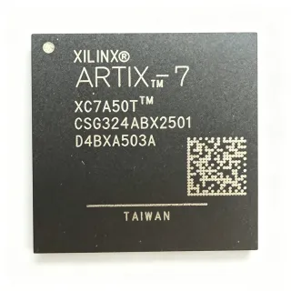
XC6SLX25-N3CSG324C - Spartan-6 FPGA, 24051 Cells | AMD
MPN: XC6SLX25-N3CSG324C ✓ Active| Qty | Unit Price | Extended |
|---|---|---|
| 1 | $45.2 | $45.20 |
| 10 | $41.8 | $418.00 |
| 100 | $36.5 | $3,650.00 |
| 500 | $32.9 | $16,450.00 |
| 1,000 | $29.4 | $29,400.00 |
XC6SLX25-N3CSG324C Overview
An FPGA (Field Programmable Gate Array) is an integrated circuit that can be programmed after manufacturing to implement any digital logic function. FPGAs consist of configurable logic blocks (CLBs), programmable interconnects, and I/O blocks, allowing designers to create custom hardware without the cost and lead time of ASIC development. The Spartan-6 family sits within the broader FPGA hierarchy, positioned as a cost-optimized line below the higher-performance Virtex and Kintex families, making it ideal for applications where price and power are critical.
Key features of the XC6SLX25-N3CSG324C include 1,879 CLBs, 38 DSP48A1 slices for digital signal processing, and support for a wide range of I/O standards through SelectIO technology. The device also includes enhanced mixed-mode clock management (MMCM) blocks for precise clock generation, and supports configuration via JTAG, SPI, and BPI interfaces. With a junction temperature range of 0°C to 85°C, this commercial-grade FPGA is suitable for typical industrial and consumer environments.
The Spartan-6 architecture incorporates advanced power management modes, including suspend and hibernate states, to reduce static power consumption. The 45nm process technology enables high logic density while maintaining low dynamic power, making the XC6SLX25-N3CSG324C an energy-efficient choice for battery-powered or thermally constrained designs. Additionally, the device supports AES bitstream encryption and Device DNA protection for enhanced IP security.
Typical applications for the XC6SLX25-N3CSG324C include motor control, industrial networking, video processing, and software-defined radio. Its 226 I/O pins and 324-ball package provide ample connectivity for interfacing with sensors, ADCs, DACs, and communication transceivers. The FPGA's reconfigurability allows for rapid prototyping and field updates, reducing time-to-market.
When designing with this FPGA, careful attention must be paid to power supply decoupling and PCB layout to ensure signal integrity at high I/O speeds. The device requires a 1.2V core supply and 2.5V/3.3V auxiliary supplies, with proper sequencing as specified in the datasheet. Thermal management is also important, as the CSBGA package has a thermal resistance that must be considered for high-utilization designs.
Drop-in alternatives for XC6SLX25-N3CSG324C — same package, pin-to-pin compatible. Different-package parts requiring PCB rework are excluded.
Quick Comparison Tool — Select alternative parts for side-by-side comparison:
XC6SLX25-N3CSG324I
✅ Drop-In📋 Reference alternative (not in catalog)
XC6SLX25-2CSG324C
✅ Drop-In ⚠️ Specs Unverified📋 Reference alternative (not in catalog)
XC6SLX25-3CSG324C
✅ Drop-In ⚠️ Specs Unverified📋 Reference alternative (not in catalog)
XC6SLX45-2CSG324C
✅ Drop-In📋 Reference alternative (not in catalog)
XC6SLX45-N3CSG324C
✅ Drop-In ⚠️ Specs Unverified📋 Reference alternative (not in catalog)
XC6SLX25-N3CSG324C Maximum Ratings & Electrical Characteristics
| Family | Spartan-6 LX |
| Logic Cells | 24051 |
| Logic Blocks (CLBs) | 1879 |
| User I/O Pins | 226 |
| Total RAM Bits | 958464 |
| DSP48A1 Slices | 38 |
| Core Supply Voltage | 1.2V (1.14V to 1.26V) |
| Operating Junction Temperature | 0°C to 85°C |
| Package | 324-LFBGA, CSPBGA (CSG324) |
| Mounting Type | Surface Mount |
| Process Technology | 45nm |
| Configuration Interfaces | JTAG, SPI, BPI |
| Clock Management | Enhanced Mixed-Mode Clock Management (MMCM) |
| I/O Standards | SelectIO (LVCMOS, LVDS, etc.) |
| RoHS Status | Compliant |
XC6SLX25-N3CSG324C Pin Configuration
| Pin A1 | IO_L1P_0 — User I/O bank 0, differential pair P |
| Pin A2 | IO_L1N_0 — User I/O bank 0, differential pair N |
| Pin B1 | IO_L2P_0 — User I/O bank 0, differential pair P |
| Pin B2 | IO_L2N_0 — User I/O bank 0, differential pair N |
| Pin C1 | VCCAUX — Auxiliary supply voltage (2.5V/3.3V) |
| Pin C2 | GND — Ground |
| Pin D1 | IO_L3P_0 — User I/O bank 0, differential pair P |
| Pin D2 | IO_L3N_0 — User I/O bank 0, differential pair N |
| Pin E1 | VCCINT — Core supply voltage (1.2V) |
| Pin E2 | GND — Ground |
| Pin F1 | IO_L4P_0 — User I/O bank 0, differential pair P |
| Pin F2 | IO_L4N_0 — User I/O bank 0, differential pair N |
Typical Applications
XC6SLX25-N3CSG324C is suitable for 6 applications: Motor Control, Industrial Networking, Video Processing, Software-Defined Radio, Medical Imaging, Aerospace and Defense.
Motor Control
The XC6SLX25-N3CSG324C provides 38 DSP48A1 slices and 226 I/O pins, making it ideal for implementing field-oriented control (FOC) algorithms for brushless DC motors. Its 45nm process ensures low power dissipation, while the 1.2V core supply reduces heat in compact drives. The FPGA's parallel processing capability allows simultaneous current sensing and PWM generation, improving control loop bandwidth. With support for multiple I/O standards, it interfaces directly with gate drivers and current sensors, reducing external logic.
Recommended
Industrial Networking
With 226 user I/O pins and support for various I/O standards, the XC6SLX25-N3CSG324C can implement Ethernet, PROFINET, or EtherCAT interfaces. Its 958,464 RAM bits provide ample buffering for packet processing, while the MMCM blocks generate precise clock domains for different protocols. The FPGA's reconfigurability allows field updates to support evolving standards. The 45nm process ensures reliable operation in industrial temperature environments (0°C to 85°C) with proper cooling.
Recommended
Video Processing
The XC6SLX25-N3CSG324C's 38 DSP48A1 slices and 958,464 RAM bits enable real-time video processing tasks such as scaling, color space conversion, and edge detection. Its 226 I/O pins can interface with parallel video buses (e.g., RGB, YUV) and memory controllers. The FPGA's parallel architecture processes multiple pixels per clock cycle, achieving high throughput. The 1.2V core supply minimizes power consumption in portable video devices, while the CSG324 package's small footprint fits space-constrained designs.
Recommended
Software-Defined Radio
The XC6SLX25-N3CSG324C is well-suited for software-defined radio (SDR) due to its DSP slices and high-speed I/O. It can implement digital down/up conversion, filtering, and modulation/demodulation algorithms. The 45nm process provides low power consumption for battery-operated radios. With 226 I/O pins, it interfaces with high-speed ADCs and DACs. The FPGA's reconfigurability allows dynamic waveform changes, making it ideal for cognitive radio applications.
Recommended
Medical Imaging
In medical imaging systems like ultrasound, the XC6SLX25-N3CSG324C can process beamforming and image enhancement algorithms. Its DSP slices handle complex arithmetic, while the 958,464 RAM bits store intermediate data. The FPGA's low power consumption is critical for portable devices. The 0°C to 85°C temperature range is suitable for clinical environments. The 226 I/O pins connect to sensor arrays and display interfaces, enabling compact system design.
Recommended
Aerospace and Defense
The XC6SLX25-N3CSG324C is used in aerospace applications for sensor fusion, communication, and control. Its 45nm process provides radiation tolerance suitable for many missions. The FPGA's reconfigurability allows in-flight updates. With 226 I/O pins, it interfaces with various sensors and actuators. The commercial temperature range limits use to controlled environments, but the 'I' version is available for wider ranges. The small CSG324 package saves weight and space in avionics.
Recommended
Recommended Products Summary
Engineering reference data for XC6SLX25-N3CSG324C — comparison, design guidance, and compliance information.
Selection Guide
Comparison with Alternatives
| Parameter | This Product | XC6SLX25-N3CSG324I | XC6SLX25-2CSG324C | XC6SLX45-2CSG324C |
|---|---|---|---|---|
| Package | 324-CSBGA (CSG324) | 324-CSBGA (CSG324) | 324-CSBGA (CSG324) | 324-CSBGA (CSG324) |
| Brand | AMD | AMD | AMD | AMD |
| Logic Cells | 24051 | 24051 | 24051 | 43661 |
| User I/O Pins | 226 | 226 | 226 | 218 |
| RAM Bits | 958464 | 958464 | 958464 | 2138112 |
| Speed Grade | -3 | -3 | -2 | -2 |
| Temperature Range | 0°C to 85°C | -40°C to 100°C | 0°C to 85°C | 0°C to 85°C |
| Core Supply Voltage | 1.2V | 1.2V | 1.2V | 1.2V |
Key Differentiators
- Highest speed grade (-3) in the Spartan-6 LX25 family (vs XC6SLX25-2CSG324C)
- Commercial temperature range optimized for cost (vs XC6SLX25-N3CSG324I)
- Balanced logic-to-I/O ratio (vs XC6SLX45-2CSG324C)
Design Notes
The XC6SLX25-N3CSG324C requires a 1.2V core supply (VCCINT) and auxiliary supplies (VCCAUX) of 2.5V or 3.3V. Use low-impedance power planes and place decoupling capacitors (0.1uF and 1uF) close to each power pin. Follow the power sequencing requirements in the Spartan-6 datasheet (DS162) to avoid latch-up or damage.
For the CSG324 package, use a 4-layer or more PCB with dedicated ground and power planes. Ensure the ball pitch (0.8mm) is compatible with your PCB design rules. Route high-speed I/O with controlled impedance (e.g., 50 ohm single-ended, 100 ohm differential) and minimize trace lengths to reduce signal integrity issues.
The CSG324 package has a thermal resistance (theta_JA) of approximately 20°C/W. For high-utilization designs, calculate power dissipation and ensure junction temperature stays below 85°C. Use thermal vias under the package and consider a heatsink or forced airflow if needed.
Compliance Information
RoHS compliant per AMD product page. Not AEC-Q100 qualified as it is not an automotive-grade device.