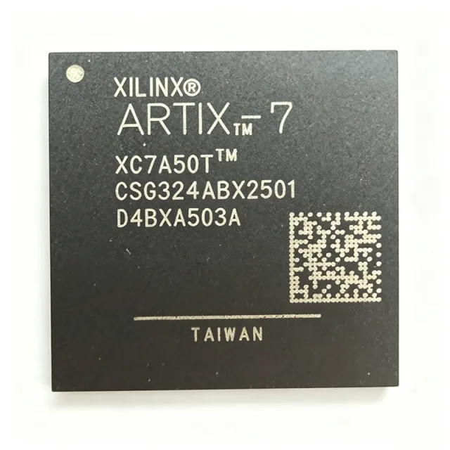
XC7A50T-2CSG324I - Artix-7 FPGA, 52K Logic Cells | AMD
MPN: XC7A50T-2CSG324I ✓ Active| Qty | Unit Price | Extended |
|---|---|---|
| 1 | $43.6364 | $43.64 |
| 10 | $31.5152 | $315.15 |
| 100 | $27.8788 | $2,787.88 |
| 500 | $26.6667 | $13,333.35 |
| 1,000 | $25.4545 | $25,454.50 |
XC7A50T-2CSG324I Overview
An FPGA (Field-Programmable Gate Array) is an integrated circuit that can be configured by the designer after manufacturing, allowing for custom digital logic implementations. FPGAs sit between ASICs (application-specific) and microprocessors (software-programmable) in the design spectrum, offering hardware-level parallelism and reconfigurability. The Artix-7 family is optimized for low power and cost at 28nm, targeting applications that require high performance per watt without the expense of high-end FPGAs.
Key features of the XC7A50T-2CSG324I include 120 DSP48E1 slices for signal processing, 5 clock management tiles (CMTs) with MMCM and PLL, and support for various I/O standards including LVCMOS, LVDS, and HSTL. The -2 speed grade provides a balance of performance and power, with the device supporting configuration via JTAG, SPI, or BPI interfaces. The CSG324 package offers a compact footprint with 324 balls on a 0.8mm pitch, enabling dense PCB layouts.
Architecturally, the Artix-7 fabric uses a 6-input look-up table (LUT) architecture with dedicated carry chains, making it efficient for both control logic and datapath designs. The integrated block RAM can be configured in various aspect ratios, and the DSP48E1 slices support multiply-accumulate operations essential for digital signal processing. The device also includes analog-to-digital converter (XADC) functionality for on-chip temperature and voltage monitoring.
Typical applications include software-defined radio, motor control, industrial networking, and medical imaging. The combination of low power, moderate logic density, and transceiver-less design makes it suitable for cost-sensitive, high-volume applications where high-speed serial links are not required.
When designing with this FPGA, careful attention must be paid to power supply decoupling on VCCINT, VCCBRAM, and VCCO rails, as well as proper configuration pin termination. The device supports partial reconfiguration, enabling dynamic updates to logic functions in the field.
Drop-in alternatives for XC7A50T-2CSG324I — same package, pin-to-pin compatible. Different-package parts requiring PCB rework are excluded.
Variants in this series
Same-series models that are drop-in compatible with XC7A50T-2CSG324I (same form factor and footprint) — differing in DSP Slices, Package, Speed Grade.
Quick Comparison Tool — Select alternative parts for side-by-side comparison:
XC7A50T-1CSG324I
✓ In Stock
$60.2 / Unit
View Datasheet →XC7A100T-2CSG324I
✓ In Stock
$105 / Unit
View Datasheet →XC7A50T-2CSG325I
✓ In Stock
$28.4 / Unit
View Datasheet →XC7A50T-2CSG324C
📋 Reference alternative (not in catalog)
XC7A50T-2FTG256I
📋 Reference alternative (not in catalog)
XC7A50T-2CSG324I Maximum Ratings & Electrical Characteristics
| Family | Artix-7 |
| Logic Cells | 52,160 |
| Block RAM | 2,764,800 bits |
| DSP Slices | 120 (DSP48E1) |
| User I/O | 210 |
| Package | 324-LFBGA, CSPBGA (CSG324) |
| Process Technology | 28nm |
| Core Voltage (VCCINT) | 1.0V |
| Speed Grade | -2 |
| Temperature Range | Industrial (-40°C to +100°C) |
| Configuration Interfaces | JTAG, SPI, BPI |
| Clock Management Tiles | 5 (MMCM + PLL) |
| RoHS Status | Compliant |
| Mounting Type | Surface Mount |
| I/O Standards | LVCMOS, LVDS, HSTL, etc. |
XC7A50T-2CSG324I Pin Configuration
| Pin A1 | IO_L1P_T0 — User I/O, differential pair P |
| Pin A2 | IO_L1N_T0 — User I/O, differential pair N |
| Pin B1 | VCCINT — Core logic power supply (1.0V) |
| Pin B2 | GND — Ground |
| Pin C1 | IO_L2P_T0 — User I/O, differential pair P |
| Pin C2 | IO_L2N_T0 — User I/O, differential pair N |
| Pin D1 | VCCBRAM — Block RAM power supply (1.0V) |
| Pin D2 | GND — Ground |
| Pin E1 | IO_L3P_T0 — User I/O, differential pair P |
| Pin E2 | IO_L3N_T0 — User I/O, differential pair N |
| Pin F1 | VCCO_0 — I/O bank 0 supply voltage |
| Pin F2 | GND — Ground |
Typical Applications
XC7A50T-2CSG324I is suitable for 6 applications: Software-Defined Radio, Motor Control, Industrial Networking, Medical Imaging, Test and Measurement, Aerospace and Defense.
Software-Defined Radio
The XC7A50T-2CSG324I is ideal for software-defined radio (SDR) due to its 120 DSP48E1 slices and 2.7 Mb block RAM, enabling digital down-conversion, filtering, and modulation. Its 210 user I/O support high-speed ADC/DAC interfaces via LVDS, while the -2 speed grade provides sufficient performance for wideband signals. The low power consumption at 28nm makes it suitable for portable and battery-operated SDR platforms, balancing processing capability with thermal constraints.
Recommended
Motor Control
In motor control applications, the XC7A50T-2CSG324I excels with its 120 DSP slices for implementing FOC (Field-Oriented Control) algorithms and PWM generation. The 210 I/O pins can interface with multiple encoder inputs and gate driver signals. The industrial temperature range (-40°C to +100°C) ensures reliable operation in factory environments. Its deterministic, low-latency fabric is ideal for real-time current and speed loops, outperforming MCU-based solutions in multi-axis systems.
Recommended
Industrial Networking
The XC7A50T-2CSG324I supports industrial networking protocols like EtherCAT and PROFINET through its flexible I/O and logic fabric. With 52K logic cells, it can implement protocol stacks, packet processing, and time-sensitive networking (TSN) features. The 28nm process ensures low power for 24/7 operation in factory settings. Its 210 I/O allow connection to multiple PHYs and backplane interfaces, making it a cost-effective choice for industrial switches and gateways.
Recommended
Medical Imaging
For medical imaging systems like ultrasound and CT scanners, the XC7A50T-2CSG324I provides the logic density and DSP capability for beamforming, image filtering, and data preprocessing. Its 120 DSP48E1 slices handle multiply-accumulate operations efficiently, while block RAM buffers image data. The industrial temperature range and RoHS compliance meet medical device requirements. The low power consumption reduces cooling needs in compact medical equipment, and the FPGA's reconfigurability allows algorithm updates without hardware changes.
Recommended
Test and Measurement
The XC7A50T-2CSG324I is well-suited for test and measurement equipment such as logic analyzers and signal generators. Its 210 I/O can capture parallel data buses, while the logic fabric implements trigger logic, data acquisition, and pattern generation. The -2 speed grade supports sampling rates up to several hundred MHz. The 28nm low-power process allows fanless designs in benchtop instruments. The FPGA's reconfigurability enables firmware updates to add new measurement features without hardware redesign.
Recommended
Aerospace and Defense
In aerospace and defense applications, the XC7A50T-2CSG324I offers the industrial temperature range and reliability needed for avionics and UAV systems. Its 52K logic cells can implement sensor fusion, navigation algorithms, and secure communication protocols. The 28nm process provides high performance per watt, critical for power-constrained airborne platforms. The FPGA's radiation-tolerant design (with appropriate mitigation) and long-term availability make it suitable for defense programs requiring stable supply chains.
Recommended
Recommended Products Summary
Engineering reference data for XC7A50T-2CSG324I — comparison, design guidance, and compliance information.
Selection Guide
Comparison with Alternatives
| Parameter | This Product | XC7A50T-1CSG324I | XC7A50T-2CSG324C | XC7A100T-2CSG324I | XC7A50T-2CSG325I |
|---|---|---|---|---|---|
| Package | 324-CSPBGA (CSG324) | 324-CSPBGA (CSG324) | 324-CSPBGA (CSG324) | 324-CSPBGA (CSG324) | 324-CSPBGA (CSG325) |
| Brand | AMD | AMD | AMD | AMD | AMD |
| Logic Cells | 52,160 | 52,160 | 52,160 | 101,440 | 52,160 |
| Block RAM (bits) | 2,764,800 | 2,764,800 | 2,764,800 | 4,860,000 | 2,764,800 |
| DSP Slices | 120 | 120 | 120 | 240 | 120 |
| User I/O | 210 | 210 | 210 | 210 | 210 |
| Speed Grade | -2 | -1 | -2 | -2 | -2 |
| Temperature Range | Industrial (-40°C to +100°C) | Industrial (-40°C to +100°C) | Commercial (0°C to +85°C) | Industrial (-40°C to +100°C) | Industrial (-40°C to +100°C) |
Key Differentiators
- Higher speed grade than -1 variant (vs XC7A50T-1CSG324I)
- Industrial temperature range (vs XC7A50T-2CSG324C)
- Lower cost and power than XC7A100T (vs XC7A100T-2CSG324I)
Design Notes
The XC7A50T-2CSG324I requires multiple power rails: VCCINT (1.0V), VCCBRAM (1.0V), and VCCO (1.2V-3.3V depending on I/O bank). Use low-dropout regulators or switching converters with adequate decoupling. Place 100nF ceramic capacitors close to each power pin and a 10uF bulk capacitor per rail. Follow AMD UG483 for power distribution system design.
The CSG324 package has a 0.8mm ball pitch, requiring careful PCB layout. Use blind/buried vias if possible to route signals between balls. Ensure the thermal pad is connected to a solid ground plane for heat dissipation. Follow AMD's PCB design guidelines in UG483 for stack-up and impedance control.
Ensure configuration pins (MODE pins) are properly terminated to select the desired configuration interface (JTAG, SPI, BPI). Do not leave unused I/O pins floating; set them to a defined state in the bitstream. Verify that VCCO for each bank matches the voltage of connected devices to avoid damage. Also, ensure VCCINT and VCCBRAM are connected to the same supply if operating at the same voltage.
Compliance Information
RoHS compliant per Veswin Electronics data. AEC-Q100 not applicable for FPGA. Other compliance data not specified in verified sources.







