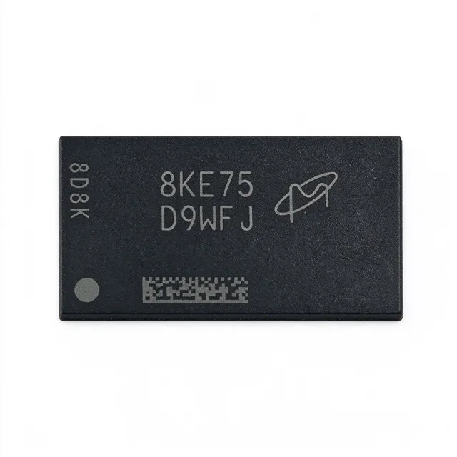
MT40A512M16LY-062E - 8Gb DDR4 SDRAM 3200MT/s | Micron
MPN: MT40A512M16LY-062E ✓ 啟用中| 數量 | 單價 | 小計 |
|---|---|---|
| 1 | $8.75 | $8.75 |
| 10 | $8.2 | $82.00 |
| 100 | $7.6 | $760.00 |
| 500 | $7.1 | $3,550.00 |
| 1,000 | $6.65 | $6,650.00 |
MT40A512M16LY-062E 概覽
DDR4 SDRAM (fourth-generation Double Data Rate Synchronous Dynamic Random-Access Memory) is a volatile memory that transfers data on both edges of the clock, doubling effective data rate versus SDR DRAM. Within the memory hierarchy it sits as the main-system-memory class of DRAM, below caches and above storage, and succeeds DDR3 with lower operating voltage and higher densities. DDR4 runs its core and I/O at VDD = VDDQ = 1.2V +/- 60mV, down from DDR3's 1.5V, cutting dynamic power while enabling higher speeds and per-device capacity up to 16Gb.
Key features of this device include 16 internal banks grouped in 2 bank groups of 4 (x16 configuration), on-die internal adjustable VREFDQ generation that simplifies memory-controller design, and 1.2V pseudo open-drain I/O. The IT industrial temperature grade supports a refresh window of 8192 cycles at 64ms for -40C to +85C, 32ms for >85C to +95C, and 16ms beyond 95C. VPP is supplied at 2.5V (-125mV/+250mV) exclusively for cell bootstrap pumping.
Advanced capability set includes auto self-refresh, write leveling, dynamic on-chip termination (ODT), CRC and CA parity support, data mask, auto precharge, asynchronous reset, and ZQ calibration via an external 240-ohm reference resistor.
Typical applications are industrial embedded controllers, networking equipment line cards, and high-performance computing or data-center memory subsystems where 3200 MT/s bandwidth per device and industrial temperature range are required.
Design-wise, plan controlled-impedance fly-by routing, 1.2V and 2.5V rails with adequate decoupling, and connect the ZQ ball to ground through exactly 240 ohms; the controller must support 2tCK ODT updates at this speed grade.
This page adds distributor pricing tiers, drop-in alternatives across Micron, Nanya, Samsung, and SK hynix, plus practical DDR4 design notes not found in the manufacturer datasheet alone.
直接替換替代品,適用於 MT40A512M16LY-062E — 相同封裝,腳位對腳位相容。需重新設計 PCB 的不同封裝零件不列入。
此系列的變體
與下列產品可直接替換的同系列型號: MT40A512M16LY-062E (相同外形與佔位) — 差異在於 Data Rate, Package, Clock Frequency, I/O Interface, Memory Size.
快速比較工具 — 選擇替代零件進行並排比較:
MT40A512M16TD-062E
✓ 有庫存
$49.2188 / 單位
查看資料表 →MT40A512M16TB-062E
✗ 缺貨
$60 / 單位
查看資料表 →MT40A512M16LY-075:E
聯絡詢價
查看資料表 →MT40A512M16HA-083E
聯絡詢價
查看資料表 →AS4C512M16D4A-62BCN
聯絡詢價
查看資料表 →NT5AD512M16A4-HR
聯絡詢價
查看資料表 →K4A8G165WC-BCWE
✗ 缺貨
$38 / 單位
查看資料表 →MT40A512M16LY-062E 最大額定值與電氣特性
| 記憶體類型 | DDR4 SDRAM |
| 記憶體容量 | 8 Gbit |
| 組織 | 512M x 16 |
| 資料速率 | 3200 MT/s |
| Clock Frequency | 1.6 GHz |
| Access Time | 19 ns |
| Supply Voltage VDD/VDDQ | 1.2 V +/- 60 mV |
| Supply Voltage VPP | 2.5 V (-125 mV, +250 mV) |
| Bank Architecture | 16 banks in 2 groups of 4 (x16) |
| Refresh | 8192-cycle; 64 ms at -40C to +85C, 32 ms >85C to +95C, 16 ms >95C |
| I/O Interface | 1.2 V pseudo open-drain |
| 功能特色 | Auto self-refresh, write leveling, dynamic ODT, CRC, data mask, auto precharge, async reset, ZQ calibration, on-die adjustable VREFDQ |
| 工作溫度 | -40C to +95C (IT grade) |
| 封裝 | 96-ball FBGA (7.5 x 13.5 mm) |
| 安裝類型 | Surface Mount |
| RoHS 狀態 | Compliant |
MT40A512M16LY-062E 96-ball fbga (7.5 x 13.5 mm) 腳位配置指南
MT40A512M16LY-062E(96-ball fbga (7.5 x 13.5 mm) 封裝)的腳位配置。 此數位 IC 包含 GPIO、通訊介面(UART、SPI、I2C)與電源腳位。替代腳位功能與配置選項請參閱製造商資料表。對嵌入式系統設計與 PCB 佈局至關重要。

無詳細腳位定義資料: MT40A512M16LY-062E.
請參閱 資料表 以查看完整腳位配置。
典型應用
MT40A512M16LY-062E 適用於 6 應用s: Industrial Embedded Controllers, Server and Data Center Memory, Networking Equipment, Automotive Infotainment and ADAS, High-Performance Computing (HPC) and GPU Accelerators, Test and Measurement Instrumentation.
Industrial Embedded Controllers
The IT industrial temperature grade (-40C to +95C) with 64 ms refresh at -40C to +85C and derated 32 ms refresh to +95C makes the MT40A512M16LY-062E well suited to industrial PLCs, machine-vision controllers, and edge-compute gateways exposed to wide ambient swings. Its 3200 MT/s data rate supplies roughly 25.6 Gbit/s per device over the 16-bit bus, enough for frame buffers and real-time data logging, while on-die VREFDQ generation removes one external reference design burden in dense multi-chip layouts. Placed in a fly-by DDR4 topology behind a controller such as an FPGA or SoC hard memory controller with 8-16 devices, it trades slightly tighter timing margins for industrial robustness; dynamic ODT and write leveling compensate for long trace runs typical of industrial backplanes.
推薦
Server and Data Center Memory
In server DIMM and memory-module designs, the MT40A512M16LY-062E provides 8Gb per device in x16 organization, allowing 16-device modules to reach 16 GB per rank with a wide 128-bit physical interface. DDR4-3200 operation delivers 25.6 Gbit/s per device, and the 2-bank-group architecture at this density doubles effective bank-level parallelism, reducing effective read latency versus DDR3 at equivalent clocks. CRC and CA parity on the command/address bus protect against bit errors on high-count fly-by loads, a requirement for registered and load-reduced module environments. Designers should budget the derated refresh window when operating above 85C in dense chassis, since the 32 ms window (8192-cycle) forces tighter refresh scheduling in the memory controller, slightly reducing effective bandwidth at sustained high ambient temperatures.
推薦
Networking Equipment
Switch, router, and network-appliance line cards use the MT40A512M16LY-062E for packet buffers, deep flow tables, and QoS queues where 8Gb density in a 7.5 x 13.5 mm footprint maximizes capacity per square centimeter. The 3200 MT/s rate with 16-bit bus yields 3.2 GB/s per device; four devices give 12.8 GB/s, sufficient for 25-100G line-rate processing with an NPUs companion SRAM for lookup tables. The asynchronous reset ball allows the system FPGA or switch ASIC to force the DRAM to a known state during hot-swap or error recovery without cycling the 1.2V rail, and ZQ calibration (240-ohm reference) keeps ODT driver impedances matched across temperature, preserving eye margins on the long backplane-class traces typical of networking hardware.
推薦
Automotive Infotainment and ADAS
For automotive platforms, the AUT:E variant of the same die (MT40A512M16LY-062E AUT:E) extends operation to +105C and carries Micron's automotive-grade qualification, making the footprint-compatible family suitable for infotainment head units, digital cockpits, and ADAS sensor-fusion ECUs. The x16 organization matches the 16-bit DDR4 interfaces common on automotive SoCs, and 8Gb density supports dual 1080p displays plus surround-camera buffering. The 16 ms refresh window above 95C (IT spec; AUT supports equivalent extended ranges) must be budgeted in the SoC memory controller for cabin environments, but pseudo open-drain I/O at 1.2V keeps per-device power low, easing thermal design in sealed, fanless automotive enclosures.
推薦
High-Performance Computing (HPC) and GPU Accelerators
Accelerator cards and HPC co-processor boards benefit from the MT40A512M16LY-062E's per-device bandwidth of 25.6 Gbit/s and the bank-group interleaving that sustains near-peak efficiency at DDR4-3200. A ring of eight x16 devices on a 128-bit bus yields 51.2 GB/s aggregate, suitable for AI inference weight storage, scientific scratch memory, and FPGA-based compute boards. On-die adjustable VREFDQ training simplifies bring-up at high data rates by letting the controller center the reference per device, and write leveling plus dynamic ODT maintain signal integrity across the heavily loaded command/address tree of 16-device stacks. CRC and CA parity add error containment critical to long-running HPC jobs that cannot tolerate silent DRAM command corruption.
推薦
Test and Measurement Instrumentation
Oscilloscopes, logic analyzers, and arbitrary waveform generators need deep capture memory with industrial temperature tolerance and predictable latency; the MT40A512M16LY-062E supplies 8Gb of streaming buffer per device at 3.2 GB/s sustained write bandwidth. The IT grade -40C to +95C range supports bench instruments destined for unconditioned environments, and the data mask function allows partial updates of the capture buffer without read-modify-write cycles, preserving sustained write throughput. Designers should place decoupling within 2 mm of VDDQ balls and use the asynchronous reset for deterministic instrument-arm sequencing. Because 3200 MT/s fly-by routing demands controlled impedance, a four-layer minimum stack with dedicated 1.2V and 2.5V VPP planes is recommended for compact instrument boards.
推薦
推薦產品摘要
工程參考資料,適用於 MT40A512M16LY-062E — 比較、設計指引及合規資訊。
選型指南
與替代品比較
| 參數 | 本產品 | MT40A512M16TD-062E | MT40A512M16TB-062E | AS4C512M16D4A-62BCN | NT5AD512M16A4-HR | K4A8G165WC-BCWE |
|---|---|---|---|---|---|---|
| Package | 96-FBGA (7.5x13.5) | 96-FBGA (7.5x13.5) - same | 96-FBGA (7.5x13.5) - same | 96-FBGA (7.5x13.5) - same | 96-FBGA (7.5x13.5) - same | 96-FBGA (7.5x13.5) - same |
| Brand | Micron Technology | Micron Technology | Micron Technology | Alliance Memory | Nanya Technology | Samsung Electronics |
| Memory Size | 8 Gbit | 8 Gbit | 8 Gbit | 8 Gbit | 8 Gbit | 8 Gbit |
| Organization | 512M x 16 | 512M x 16 | 512M x 16 | 512M x 16 | 512M x 16 | 512M x 16 |
| Data Rate | 3200 MT/s | 3200 MT/s | 3200 MT/s | 3200 MT/s | 3200 MT/s | 3200 MT/s (CL22) |
| Supply Voltage (VDD/VDDQ) | 1.2 V +/- 60 mV | 1.2 V +/- 60 mV | 1.2 V +/- 60 mV | 1.2 V | 1.2 V | 1.2 V |
| Die Revision | LY:E | TD (newer) | TB (newer, different package supplier) | Alliance in-house die | Nanya in-house die | Samsung in-house die |
主要差異化特點
- Industrial IT temperature grade to +95C with defined derated refresh (對比K4A8G165WC-BCWE)
- Available automotive sibling with identical footprint (對比AS4C512M16D4A-62BCN)
- Newer die revisions (TD/TB) available as pin-identical successors (對比MT40A512M16LY-062E (this part, LY die))
設計說明
Route the DDR4 interface as a fly-by topology for address/command/control with per-DQS point-to-point data lanes. Maintain controlled impedance (approximately 40 ohm for command/address, 50 ohm single-ended data, 100 ohm differential for DQS_t/DQS_c) and keep length matching within the controller's skews window. The 96-FBGA land pattern is the industry-standard JEDEC DDR4 x16 map, so designs can accept TD, TB, or cross-brand alternatives without layout changes.
Provide two supply rails: VDD = VDDQ = 1.2V +/-60mV and VPP = 2.5V (-125mV/+250mV). VPP carries only peak cell-bootstrap current but must stay in regulation or cells lose retention margin. Decouple VDD/VDDQ with dense 100 nF capacitors within 2 mm of supply balls plus bulk capacitance per rail. Estimated: a 16-device module at 3200 MT/s can draw several amps peak on the 1.2V rail, so plan PDN impedance accordingly in the controller's DIMM budget.
Connect the ZQ ball to ground through exactly a 240-ohm, 1% resistor; a wrong value skews all output driver and ODT impedances and collapses eye margins at 3200 MT/s. Above 85C the refresh window halves (64 ms to 32 ms per 8192 cycles), and above 95C it is 16 ms - memory-controller refresh scheduling must be configured for the actual operating temperature or data retention errors occur. Also verify mode-register programming compatibility when second-sourcing TB/TD die revisions.
Enable write leveling and dynamic ODT during controller training; these features are mandatory in practice at DDR4-3200 with multi-device loads. On-die adjustable VREFDQ lets the controller center the DQ reference per device during training - do not hard-code VREF values from an older DDR3 design. Simulate fly-by stub lengths and CA bus eye at the full 16-device load before release; CA parity/CRC helps contain residual command errors but does not replace margin.
合規資訊
RoHS compliant per distributor listings (DigiKey/LCSC). Industrial IT grade part - not automotive qualified; use the AUT:E variant for automotive. REACH and conflict-minerals status not stated in provided data.




