FPGA & CPLD
Products (6352)
10CX105YF780E5G - Cyclone 10 GX FPGA, 105K LE, 780-BGA | Intel
The Intel 10CX105YF780E5G is a Cyclone 10 GX field-programmable gate array (FPGA) with 105,000 logic elements, 8,641,536 bits of embedded memory, and 284 user I/Os, fabricated on a 20 nm process and housed in a 780-ball flip-chip BGA (FCBGA) package. It belongs to the Cyclone 10 GX family, which targets mid-range applications requiring transceivers, DSP blocks, and low-power operation. The 'E5' speed grade and '0C' (commercial, 0 to 100 C) temperature rating make this part suitable for cost-sensitive, non-automotive designs. The 'F780' suffix indicates the 780-ball FCBGA package, while 'Y' denotes the transceiver-equipped variant with 12.5 Gbps GX transceivers. An FPGA (Field-Programmable Gate Array) is a semiconductor device containing programmable logic blocks, configurable interconnects, and dedicated hard IP blocks such as transceivers, PLLs, and DSP slices. FPGAs occupy the middle ground between fixed-function ASICs and software-driven microcontrollers: they offer hardware-level parallelism and deterministic latency for applications like video processing, industrial networking, and motor control, while still being reprogrammable in the field. Cyclone 10 GX sits within Intel's low-power FPGA portfolio, optimized for cost and power efficiency while integrating 12.5 Gbps transceivers and a hard memory controller — a feature set historically reserved for higher-end Stratix families. Key features of the 10CX105YF780E5G include 105K logic elements, 38,000 adaptive logic modules (ALMs), 8.439 Mbits of embedded SRAM, 284 user I/Os, hard 12.5 Gbps GX transceivers, variable-precision DSP blocks, and hard PCIe Gen2 controllers. The device supports DDR3 external memory interfaces up to 933 MHz, and integrates a hard floating-point arithmetic block on each DSP. Multiple PLLs and global clock networks provide flexible clock domain management. Cyclone 10 GX uses a 20 nm process with TSMC's low-power technology, enabling a typical core power of less than 1 W per 100K LE plus transceiver contribution. The hard IP for transceivers, PCIe, and memory controllers reduces soft logic overhead, freeing programmable fabric for application-specific logic. The FCBGA-780 package offers controlled-impedance signal routing for high-speed serial links. Typical applications include industrial machine vision, video broadcast and surveillance, software-defined radio, factory automation controllers, and PCIe-based accelerator cards. The combination of transceivers and low power makes Cyclone 10 GX especially attractive for fanless embedded systems with high-speed serial I/O. When designing with this device, allocate PCB stackup budget for the FCBGA's 1.0 mm ball pitch and use Intel's Quartus Prime toolchain for synthesis, place-and-route, and timing closure. Pay close attention to transceiver channel placement and reference clock routing to maintain signal-integrity at 12.5 Gbps. This page synthesizes distributor pricing, package-specific alternatives, and practical Quartus design guidance not consolidated in the official Cyclone 10 GX datasheet.
10CX105YF780E6G - Cyclone 10 GX FPGA, 104K LE, 780-FCBGA | Altera/Intel
The Altera/Intel 10CX105YF780E6G is a Cyclone 10 GX field-programmable gate array (FPGA) integrating 104,000 logic elements (LE) and 8,641,536 embedded memory bits in a 780-ball flip-chip BGA (FCBGA) package. Part of the Cyclone 10 GX family, this 20 nm device delivers up to 12.5 Gbps transceiver performance, hardware floating-point DSP blocks, and a 1.4 Gbps LVDS SERDES interface, targeting cost-sensitive applications that previously required higher-tier FPGAs. A Field-Programmable Gate Array (FPGA) is a semiconductor integrated circuit containing programmable logic blocks, configurable interconnect, and hardened I/O and memory resources. FPGAs sit in the broader taxonomy of programmable logic devices -> programmable logic -> logic ICs -> integrated circuits -> semiconductors. The Cyclone 10 GX family uses a 20 nm TSMC fabrication process and embeds dedicated transceiver and PCIe Gen2 hard IP blocks, giving system architects a balanced trade-off between low power, mid-range density, and high-speed serial connectivity compared to ASICs and CPLDs. Key features include 8,641,536 bits (approximately 8.5 Mb) of embedded SRAM, 156 18x19 multipliers (or DSP blocks), up to 284 user I/O pins, six 12.5 Gbps transceivers, and one PCIe Gen2 hard IP block. The device also integrates a hard memory controller, 3.0 Gbps external memory interface, configuration via fast passive parallel (FPP), and active serial (AS) modes. With a 1.0 V core voltage and 0.9 V auxiliary supply, the part is optimized for sub-1.5 W typical power consumption in industrial temperature operation. Architecturally, the Cyclone 10 GX uses a logic-array-block (LAB)-based fabric with adaptive logic modules (ALMs) and a multi-tier routing hierarchy. Hardened transceiver PHY blocks support protocols such as PCIe Gen1/Gen2 x1/x2/x4, 10 GbE (10GBASE-R), and CPRI. The embedded hard memory controllers support DDR3, DDR3L, and LPDDR2 external memory, allowing high-throughput buffering for video, packet processing, and DSP pipelines without consuming fabric resources. Typical applications include industrial machine vision over 10 GbE, wireless backhaul baseband preprocessing, PCIe endpoint cards, broadcast video processing, and low-cost ASIC prototyping. The combination of 12.5 Gbps transceivers, hardened PCIe, and 104K LE makes the 10CX105YF780E6G well-suited for designs where low-end Cyclone V or Spartan-6 parts lack transceivers but full Arria 10 or Kintex-7 devices are over-budget. When designing with this device, ensure signal-integrity simulation for the 12.5 Gbps serial links, and verify PCB stackup meets Intel's transceiver routing guidelines (lossy PCB channel compliance). Power-rail decoupling should follow the Intel Cyclone 10 GX Pin Connection Guidelines for proper POR and configuration sequence. This page synthesizes distributor pricing, drop-in same-package alternatives, comparison data against 10CX085/Cyclone V and Xilinx Artix-7 competitors, and PCB-layout design notes not collected in a single datasheet reference.
10CX105YF780I5G - Cyclone 10 GX FPGA 105K LE, 8.4Mb | Intel
The Intel 10CX105YF780I5G is a Cyclone 10 GX field-programmable gate array (FPGA) with 105,000 logic elements, 8,641,536 bits of embedded memory, packaged in a 780-ball FCBGA (F780) housing. It delivers 284 user I/O pins with an industrial temperature grade (-40C to +100C) and is targeted at high-throughput, low-power programmable logic applications. An FPGA (Field-Programmable Gate Array) is a semiconductor device containing programmable logic blocks, interconnect fabric, and I/O cells that the user configures after manufacture. FPGAs occupy the programmable-logic tier of the digital IC hierarchy: ASIC < FPGA < CPLD < microcontroller < standard logic. Within Intel's portfolio, Cyclone 10 GX sits in the low-power, transceiver-rich mid-range, between the smaller Cyclone 10 LP family and the high-end Stratix 10 line. Key features include 38,000 adaptive logic modules (ALMs), integrated transceivers supporting up to 12.5 Gbps, hard memory controllers, and a 0.9 V core supply. The device uses a 20 nm process and supports 1.4 Gbps LVDS, PCIe Gen2 hard IP blocks, and on-chip hardened floating-point multipliers. The 780-ball FCBGA provides the thermal envelope required for full transceiver operation at industrial temperatures. Architecturally, the 10CX105YF780I5G combines a fabric of logic elements, dedicated DSP blocks, M20K memory blocks, and a hardened PCIe Gen2 x4 controller. Transceivers and PLLs are integrated as hard IP to free fabric logic and to deliver deterministic latency for serial protocols, distinguishing the Cyclone 10 GX from soft-logic-only predecessors. Typical applications include industrial machine vision, video bridge and protocol conversion, motor control and drive, broadcast equipment, and PCIe-based data-acquisition cards. The transceiver-rich 780-ball package is well suited to designs that require multi-gigabit serial links alongside programmable logic. When designing with this device, allocate at least one transceiver reference clock and verify PCB routing for 12.5 Gbps signals. The Quartus Prime Lite design suite supports the entire Cyclone 10 GX family, and Intel provides validated reference designs for PCIe Gen2 x4 endpoint applications. This page synthesizes current distributor pricing, drop-in same-package alternatives from the Cyclone 10 GX family, and practical design notes beyond what is found in the manufacturer datasheet, supporting fast sourcing and BOM risk decisions.
10CX105YF780I6G - Cyclone 10 GX FPGA 104K LE | Intel | 780-FBGA
The Intel 10CX105YF780I6G is a Cyclone 10 GX field-programmable gate array (FPGA) with 104,000 logic elements, 8,641,536 bits of embedded memory, and 284 user I/O pins, housed in a 780-ball Flip-Chip BGA (FCBGA) package. Built on Intel's 20 nm process, this device integrates up to 1.5 Gbps LVDS and 6.144 Gbps transceiver capability, targeting high-bandwidth bridging, video connectivity, and industrial vision applications. The Industrial temperature grade (I) ensures operation from -40C to +100C ambient. An FPGA is a programmable logic device containing configurable logic blocks (CLBs), dedicated DSP blocks, embedded SRAM, and programmable I/O, all interconnected by a programmable routing fabric. FPGAs occupy a middle ground between fixed-function ASICs and general-purpose microcontrollers: they deliver hardware parallelism and deterministic latency for data-pipeline tasks while allowing full logic redesign after PCB fabrication. Within Intel's low-power Cyclone family, the Cyclone 10 GX adds hardened transceivers and an integrated protocol stack for PCI Express Gen2 and 10 GbE (10GBASE-R/KR) on the higher-density members, differentiating it from the transceiver-less Cyclone 10 LP. Key features of the 10CX105YF780I6G include 104K logic elements, 8,641,536 embedded memory bits, 156 embedded 18x18 multipliers, 1 PLL per side, and 6 transceiver channels operating up to 6.144 Gbps. The device also provides 2 hard memory controllers and 1 PCIe Gen2 hard IP block (x4 root port or endpoint). The 780-pin FCBGA package exposes 284 user I/O supporting LVDS, LVCMOS, SSTL, and HSTL I/O standards. Architecturally, the Cyclone 10 GX uses a logic-structural fabric with adaptive logic modules (ALMs) of 8-input fracturable look-up tables, fine-grained DSP blocks with pre-adder and accumulator chains, and embedded M20K memory blocks. Hardened protocol IP reduces soft-logic overhead for PCIe and Ethernet, allowing more design resources to be allocated to application logic. Typical applications include industrial machine vision over GigE Vision or CoaXPress, video broadcast contribution encoders, low-density PCIe endpoint cards, military secure radio, and FPGA-based motor control for industrial drives. Designers choose this part for moderate-density designs that require hardened transceivers without paying the power and cost of higher-end Stratix or Arria 10 devices. When designing with the 10CX105YF780I6G, engineers should plan power-rail sequencing (1.0V core, 2.5V/3.3V aux, 1.8V transceiver PLL), use a minimum of 8 PCB layers with continuous GND planes for transceiver signal integrity, and ensure thermal dissipation through the exposed die on the FCBGA. The Quartus Prime Lite or Pro toolchain is required for synthesis and place-and-route. This page synthesizes distributor pricing, drop-in alternatives from the Cyclone 10 GX family, and practical design notes not found in the manufacturer datasheet alone, helping procurement and engineering teams decide quickly whether 10CX105YF780I6G is the correct fit for their volume production.
10CX105YU484E5G - Cyclone 10 GX FPGA 104K LE 484-UBGA | Intel
The Intel (formerly Altera) 10CX105YU484E5G is a Cyclone 10 GX field-programmable gate array (FPGA) IC with 104,000 logic elements, 8,641,536 bits of embedded memory, and 188 user I/O, housed in a 484-pin U484 Ultra FineLine BGA (UBGA) package. It belongs to the Cyclone 10 GX family, Intel's low-power FPGA line optimized for bandwidth-intensive applications requiring transceivers and DSP throughput. An FPGA (Field-Programmable Gate Array) is a semiconductor integrated circuit that can be reconfigured by the customer after manufacturing. FPGAs sit in the broader category of programmable logic devices (PLDs), above simple CPLDs in density and capability. The Cyclone 10 GX family specifically targets applications that require high-speed serial transceivers, hardened floating-point DSP blocks, and external memory interfaces, while consuming substantially less power than the Stratix 10 family. Key features include 104K logic elements (LEs), 8,641,536 bits (approximately 8.2 Mbit) of total embedded RAM, 38,000 adaptive logic modules (ALMs) organized into logic array blocks (LABs), and 188 general-purpose I/O. The device integrates 6.144 Gbps transceivers, hard memory controllers, and a hard floating-point DSP subsystem, allowing parallel processing of high-throughput DSP workloads without consuming logic fabric. The 0.9 V core supply enables low static and dynamic power dissipation. The Cyclone 10 GX architecture uses a 20 nm process technology, with logic synthesized into adaptive logic modules (ALMs) each containing an 8-input fracturable look-up table (LUT), two dedicated adders, and four registers. The M20K memory blocks and variable-precision DSP blocks are hardened to deliver deterministic performance and conserve fabric resources for control logic. The hard floating-point DSP subsystem provides IEEE 754 single-precision multiply-accumulate at high block rates. Typical applications include industrial machine vision and video processing, broadcast and professional audio/video equipment, 4K UHD display interfaces, PCIe Gen2 endpoint and root-port designs, and low-cost radar/lidar preprocessing. The 484-UBGA package offers generous I/O density in a compact 19 mm × 19 mm footprint suitable for space-constrained boards. When designing with this device, ensure adequate power-rail decoupling on each of the VCC, VCCPT, VCCA_PLL, and transceiver supply groups, and follow Intel's pin connection guidelines for unused pins. Operating temperature is commercial 0°C to 100°C (TJ); choose the industrial grade variant for extended temperature operation. This page consolidates distributor pricing, drop-in same-family Cyclone 10 GX alternatives, and practical PCB design notes that go beyond the manufacturer datasheet's typical application examples.
10CX105YU484E6G - 104K LE Cyclone 10 GX FPGA 484-BGA | Intel
The Intel (formerly Altera) 10CX105YU484E6G is a high-density, low-power field-programmable gate array (FPGA) from the Cyclone 10 GX family, fabricated on a 20 nm process. The device integrates 104,000 logic elements, 8,641,536 bits of embedded memory, 188 user I/O pins, and a 12.5 Gbps transceiver subsystem, all housed in a 484-pin Ultra FineLine BGA (UBGA, 19x19 mm) package. It targets high-bandwidth, cost-sensitive applications requiring hardened transceivers, DSP blocks, and PCIe Gen2 hard IP. A field-programmable gate array (FPGA) is a reconfigurable semiconductor integrated circuit whose logic fabric, routing, and I/O can be programmed by the end user after manufacture. FPGAs sit within the programmable-logic device (PLD) hierarchy, which also includes complex programmable logic devices (CPLDs). Architecturally, an FPGA such as the Cyclone 10 GX combines look-up tables (LUTs), flip-flops, block RAM (BRAM), DSP slices, phase-locked loops (PLLs), and increasingly hard intellectual property (IP) cores such as PCIe controllers and multi-gigabit transceivers. This heterogeneity makes FPGAs preferred glue logic, accelerator, and connectivity platforms for embedded, industrial, video, and communications designs. Key differentiating features of the 10CX105YU484E6G include six 12.5 Gbps transceivers, hard PCIe Gen2 x4 IP, up to 480 DSP blocks, 188 single-ended (or 94 differential-pair) general-purpose I/Os, and 3.125 Gbps LVDS support. The device supports LPDDR2, DDR3, and DDR3L external memory interfaces with soft physical layer (PHY) IP, and offers a hardened floating-point arithmetic block set for DSP workloads. Its 20 nm process enables a low static power profile relative to prior 28 nm Cyclone generations. The 10CX105YU484E6G is a fit for high-volume applications such as industrial machine vision with GigE Vision or CoaXPress interfaces, broadcast video processing and encoding, motor control and industrial drive systems, wireless backhaul baseband, and embedded PCIe expansion cards. The integrated 12.5 Gbps transceivers remove the need for external PHY chips on most serial links. Designers targeting low-cost video, HMI, or smart-factory edge nodes benefit from the large logic capacity combined with low-power operation. For designs previously locked to Arria II or earlier, the Cyclone 10 GX delivers substantially higher DSP throughput at comparable static power. When designing in this part, engineers should budget for the device's 1.0 V core VCC supply sequencing and provide robust decoupling per Intel's Power Distribution Network (PDN) guidelines. Pin-out compatible speed-grade and density migrations exist within the Cyclone 10 GX family, allowing pin-compatible movement to lower-cost 10CX085 (85K LE) or higher-cost 10CX220 (220K LE) variants within the same UBGA-484 footprint, depending on yield. JTAG and active serial configuration via the Altera/Intel Quartus Prime toolchain are mandatory. This page synthesizes verified distributor pricing, parametric alternatives within the Cyclone 10 GX family, and practical design notes that complement but do not duplicate the manufacturer datasheet.
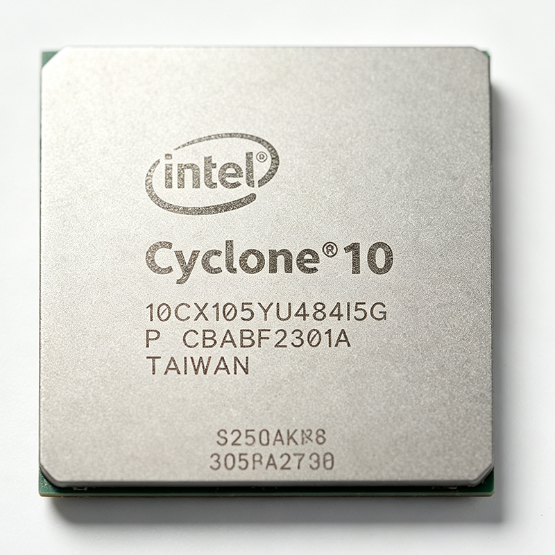
10CX105YU484I5G - 104K-Cell Cyclone 10 GX FPGA | Intel | Industrial Systems
The Intel 10CX105YU484I5G is a Cyclone 10 GX field-programmable gate array (FPGA) with 104,000 logic cells, 8,640,? [DATA_NEEDED: logic elements value] embedded memory bits, and 188 user I/O elements in a 484-pin BGA package. It is designed for configurable digital logic, high-speed interfaces, and industrial applications requiring programmable hardware. The 484-pin package designation is U484, and the ordering code includes the industrial temperature grade and speed-grade identifier I5. An FPGA is a semiconductor device whose digital logic and interconnects are configured after manufacturing. Its hierarchy is FPGA, programmable logic device, configurable logic integrated circuit, and digital semiconductor. Unlike a fixed-function ASIC, an FPGA can implement changing logic functions, interface protocols, control algorithms, and signal-processing datapaths. The Cyclone 10 GX family places programmable logic resources together with I/O and embedded functional blocks, allowing a system designer to consolidate functions that might otherwise require several connected components. The defining feature of 10CX105YU484I5G is its 104,000-cell Cyclone 10 GX architecture. The device provides 188 user I/O resources, 8,640,? [DATA_NEEDED: embedded memory value] memory resources as reported by the distributor description, and 484 package terminals. Its FPGA structure supports configurable parallel logic, serial communication, state machines, timing logic, and custom control blocks. The exact supported transceiver count, maximum operating frequency, power supply limits, and embedded block details must be confirmed from the manufacturer datasheet before final design sign-off. The 10CX105YU484I5G uses a 20 nm process technology, as identified in the distributor listing. This places the component in a high-density programmable-logic class aimed at designs that need more integration than a small CPLD or low-capacity FPGA. The package uses a 484-pin BGA footprint, so PCB escape routing, via-in-pad strategy, solder-mask definition, and signal-integrity analysis are important. The device should be treated as a complex high-speed digital component even where a particular design does not use every available I/O. Typical applications include industrial control and automation, communication equipment, test and measurement, video and image processing, and custom data-acquisition systems. These applications benefit from the ability to revise logic, support multiple interface standards, and adapt timing or protocol behavior without replacing the entire PCB. The 188 I/O resources are especially relevant to systems that aggregate sensors, control signals, memory interfaces, and management buses. When designing with this FPGA, verify all I/O-bank voltage constraints, clocking requirements, configuration architecture, power sequencing, and supported interface standards from the manufacturer documentation. The industrial-grade ordering code should be checked against the complete temperature and qualification wording in the official datasheet. This page combines verified distributor attributes, package and sourcing information, and practical engineering guidance; values not exposed by the supplied search data are explicitly marked rather than estimated.
10CX105YU484I6G - Cyclone 10 GX FPGA, 104K LE, 484-BGA | Intel
The Intel 10CX105YU484I6G is a Cyclone 10 GX field-programmable gate array (FPGA) delivering 104,000 logic elements, 8,641,536 bits of embedded memory, and 188 user I/O pins in a 484-ball Ultra FineLine BGA (UBGA) package built on a 20 nm process. The device integrates six 12.5 Gbps transceivers, hardware floating-point DSP blocks, and a 72-bit-wide DDR3 SDRAM interface supporting up to 1866 Mbps, targeting cost-sensitive applications that still require multi-gigabit serial connectivity. An FPGA is a programmable logic device whose architecture is built from an array of configurable logic blocks (CLBs), programmable routing, dedicated DSP and block-memory tiles, and high-speed serial transceivers, all wrapped by user I/O. FPGAs sit at the top of the digital-semiconductor hierarchy alongside microcontrollers and ASICs, but are distinguished by hardware-level parallelism and the ability to reconfigure logic after PCB assembly. The Cyclone 10 GX family is Intel's low-power, transceiver-equipped member of the Cyclone 10 series, balancing cost per logic element against bandwidth for video, industrial imaging, and machine-vision pipelines. Key features of the 10CX105YU484I6G include 6 transceivers at up to 12.5 Gbps, 156 DSP blocks (18x18 multipliers), 4 PLLs, 1.4 Gbps LVDS support, and a hard memory controller for external DDR3 up to 1.866 Gbps. The device is available in industrial temperature grade (-40C to 100C) with Pb-free and RoHS-compliant packaging. Typical applications include industrial machine vision, broadcast video processing, ProAV signal routing, motor control and industrial Ethernet bridging, and PCIe Gen2 endpoint designs that need a small-form-factor BGA with high I/O count. The 484-ball UBGA footprint is shared across several Cyclone 10 GX density points and package options, simplifying PCB layout reuse. When designing with this device, ensure that PCB layout meets Intel's transceiver channel guidelines (controlled-impedance routing, AC-coupling capacitors, length matching) and that the Quartus Prime power-estimation flow is run before sign-off to size decoupling capacitors and voltage-rail current. The industrial-grade variant supports extended operation but still requires the same thermal envelope as commercial parts when dissipation exceeds the package's typical theta_JA. This page synthesizes distributor pricing, same-family drop-in alternatives, and practical design notes that are not found in the standalone Intel datasheet, helping engineers shorten the sourcing and qualification cycle for Cyclone 10 GX designs.
10CX150YF672E5G - Cyclone 10 GX FPGA, 150K LE, 672-FCBGA | Intel
The Intel 10CX150YF672E5G is a Cyclone 10 GX field-programmable gate array (FPGA) integrating 150,000 logic elements, 10,907,648 bits of embedded memory, and 236 general-purpose I/O pins in a 672-ball FineLine BGA (FCBGA) package fabricated on a 20 nm process node. The device belongs to Intel's low-power, transceiver-rich Cyclone 10 GX family and supports up to 6.144 Gbps transceivers, hardware floating-point DSP blocks, and hard memory controllers for mid-range industrial, video, and wireless designs. A field-programmable gate array (FPGA) is a semiconductor device built around a matrix of configurable logic blocks (CLBs), programmable interconnects, and dedicated hardware IP such as DSP slices, block RAM (BRAM), and high-speed serial transceivers. Unlike an application-specific integrated circuit (ASIC), an FPGA's function is defined after manufacture by loading a hardware description language (HDL) bitstream into on-chip SRAM configuration memory. The Cyclone 10 GX family sits within Intel's broader programmable logic hierarchy (FPGA -> programmable logic device -> programmable logic IC -> semiconductor), targeting applications that need higher transceiver bandwidth than Cyclone 10 LP but lower static power and cost than Arria 10 or Stratix 10. Key features of the 10CX150YF672E5G include 150,000 logic elements (LEs), 156 hardware 18x19 multipliers, 490 variable-precision DSP blocks with hardened single-precision floating-point support, 8.5 Mbits of M20K block RAM plus 9.6 Mbits of MLAB memory, six 6.144 Gbps PLLs with fractional-N synthesis, 3.3 V-tolerant LVCMOS/LVDS/LVPECL general-purpose I/O, and a hard PCIe Gen2 x4 controller for embedded compute and storage interfacing. Architecturally the device combines a fine-grained LE fabric with column-based DSP and M20K memory columns, a periphery of high-speed transceivers, and a hardening of common protocol IPs (PCIe, EMIF, JTAG). The 20 nm process enables a die small enough to fit into a 672-ball FCBGA while keeping static power below 1.5 W typical, suiting fanless or limited-cooling enclosures. Typical applications include industrial machine vision and video bridging, factory automation HMI, low-density wireless backhaul modems, broadcast video processing, and PCIe-based accelerator cards. The combination of transceivers, on-chip memory, and DSP makes the part well suited to designs that previously required a discrete ASSP plus an external bridge. When designing in the 10CX150YF672E5G, allocate at least 4 PCB layers for transceiver signal integrity, follow Intel's pin connection guidelines for unused pins and JTAG pull-ups, and use the Quartus Prime Lite/Pro design suite (Cyclone 10 GX device support) for synthesis, place-and-route, and timing closure.
10CX150YF672E6G - Cyclone 10 GX 150K LE FPGA, 672-FCBGA | Intel
The Intel 10CX150YF672E6G is a Cyclone 10 GX field-programmable gate array (FPGA) offering 150,000 logic elements, 10,907,648 embedded memory bits, and 236 (18x18) multipliers in a 672-ball FCBGA package. It targets mid-range, power-sensitive applications that need transceiver-rich I/O and DSP bandwidth at industrial-grade operating conditions. The part ships as an Enhanced speed-grade (-E6G) device rated for industrial temperature operation. A Field-Programmable Gate Array (FPGA) is a reconfigurable integrated circuit that combines programmable logic blocks, routing interconnect, and hardened IP blocks such as transceivers, DSP blocks, and memory controllers. FPGAs occupy a unique position in the semiconductor hierarchy: more flexible than an application-specific standard product (ASSP) yet more deterministic and parallel than a microprocessor. The Cyclone 10 GX family specifically sits at the intersection of low static power, integrated 12.5 Gbps transceivers, and hardened PCI Express Gen2 controllers - making it a mainstream workhorse for video, industrial, and wireline bridge designs. Key features of the 10CX150YF672E6G include up to 12.5 Gbps multi-protocol transceivers, hard PCI Express Gen2 x4 IP blocks, hardened variable-precision DSP blocks supporting 18x18 multipliers and 27-bit pre-adder, and up to 10.9 Mbits of embedded SRAM distributed between M20K block memory and LUTRAM. The device is fabricated on Intel's 20 nm process, balancing leakage versus performance for thermally constrained enclosures. Per-bank programmable I/O banks support LVDS, LVCMOS, and memory interfaces up to DDR3. Architecturally, the Cyclone 10 GX uses an Adaptive Logic Module (ALM) as its basic building block - each ALM contains an 8-input fracturable look-up table, two dedicated adders, and four registers. Combined with the Core fabric, Memory, and DSP blocks, the 10CX150 delivers approximately 150K logic elements with deterministic routing and timing closure supported by the Quartus Prime design suite. Typical applications include industrial machine vision over CoaXPress or GigE Vision, broadcast video processing with 12G-SDI and DisplayPort bridging, low-cost 10G Ethernet aggregation switches, motor control and digital drive systems, and PCI Express Gen2 endpoint cards. The transceiver and hard PCIe IP blocks also suit radar/LiDAR front-end preprocessing and software-defined radio baseband. When designing with this part, pay attention to the FCBGA 672-ball pitch and PCB stack-up. Use Intel's Cyclone 10 GX pin connection guidelines to assign unused I/O, enable internal weak pull-ups where required, and follow the High Speed Board Design Guidelines for the 12.5 Gbps transceiver channels. Plan a complete Quartus Prime-based power tree early - the device uses multiple supply rails (VCC, VCCPT, VCCR_GXB, VCCT_GXB) that must be sequenced. This page synthesizes distributor pricing, drop-in package alternatives within the Cyclone 10 GX and Cyclone 10 LP families, and practical design notes not found in the manufacturer datasheet alone.
10CX150YF672I5G - Cyclone 10 GX FPGA, 150K LE, 672-FCBGA | Intel
The Intel (formerly Altera) 10CX150YF672I5G is a Cyclone 10 GX field-programmable gate array (FPGA) integrating 150,000 logic elements, 10,907,648 bits of embedded memory, and 236 user I/O pins in a 672-ball flip-chip BGA (FCBGA) package. It belongs to the low-power, transceiver-rich Cyclone 10 GX family fabricated on a 20 nm process, delivering transceiver rates up to 12.5 Gbps for cost-sensitive high-volume applications. The device operates over the industrial -40C to +100C temperature range with a 0.9 V core supply. An FPGA (Field-Programmable Gate Array) is a reconfigurable integrated circuit that combines programmable logic blocks, configurable interconnects, and dedicated DSP/memory blocks into a single silicon die. Within the broader taxonomy, an FPGA sits as a specialized subclass of programmable logic devices (PLDs) and, more generally, as an application-specific integrated circuit (ASIC) alternative under the digital semiconductor hierarchy: FPGA -> programmable logic -> logic IC -> integrated circuit. Cyclone 10 GX specifically targets cost-optimized, transceiver-enabled designs that previously required more expensive mid-range FPGAs. Key features of the 10CX150YF672I5G include up to 12.5 Gbps multi-gigabit transceivers, a hard memory controller for DDR3/DDR4/LPDDR3 external memory, PCI Express Gen2 hard IP blocks, and a 1.4 Gbps LVDS serializer/deserializer interface. The 672-FCBGA package supports high I/O count with dedicated high-speed transceiver and LVDS pairs. With 54,770 adaptive logic modules (ALMs) and 156 18x19 multipliers, the device balances logic density with DSP throughput for video bridging, machine vision, and industrial wireless backhaul. Architecturally, the Cyclone 10 GX family uses a 20 nm process with hard IP blocks for transceivers, PCIe Gen2, and external memory controllers, freeing programmable fabric for application logic. The hard transceiver PHY eliminates the soft-SERDES power penalty and reduces latency for protocols such as 10 GbE, CPRI, and JESD204B. According to Intel Cyclone 10 GX device documentation, the 150 K LE variant targets designs that need richer transceiver count and DSP than Cyclone V but do not require the higher logic capacity of Arria 10. Typical applications include industrial machine vision frame grabbers, video broadcast equipment, PCIe Gen2 endpoint cards, 5G small-cell fronthaul, low-latency financial trading, and automotive ADAS sensor aggregation. The transceiver bandwidth and PCI Express Gen2 hard IP make it well suited for line-rate 10G Ethernet switching and CPRI 4.9G wireless backhaul. The industrial temperature range supports factory floor deployment without thermal screening. When designing with this FPGA, allocate sufficient PCB area for the 672-ball FCBGA (27 mm x 27 mm, 1.0 mm ball pitch) and follow Intel's recommended PCB stack-up for impedance-controlled transceiver channels. Decoupling requirements, transceiver channel routing, and JTAG/AS configuration pin placement should follow the manufacturer pin connection guidelines. This page synthesizes distributor pricing, drop-in alternative guidance, and practical design notes not found in the manufacturer datasheet alone.
10CX150YF672I6G - Cyclone 10 GX FPGA, 150K LE, 672-BGA | Intel
The Intel 10CX150YF672I6G is a Cyclone 10 GX Field Programmable Gate Array (FPGA) delivering 150,000 logic elements, 54,770 logic array blocks, 10,907,648 bits of embedded memory, and 236 user I/Os in a 672-ball FCBGA package. Built on a low-power 20 nm process, the Cyclone 10 GX family targets cost- and power-sensitive applications that still require transceivers and hard memory controllers, with up to 6.144 Gbps transceivers supporting PCIe Gen2 x4 and external memory interfaces up to DDR3-1866. What is a Cyclone 10 GX FPGA? FPGAs are programmable logic devices containing configurable logic blocks, routing, memory blocks, DSP blocks, and hardened IP that can be rewired at silicon level after fabrication. Cyclone 10 GX sits in Intel's (formerly Altera's) low-cost, low-power product line as a bridge between the Cyclone V family and the higher-end Arria 10, inheriting transceiver and hard memory controller IP from Arria while retaining the low static and dynamic power profile expected of Cyclone-class parts. Key features include 150K logic elements (LEs), 54,770 adaptive logic modules (ALMs), 6.6 Mb of embedded SRAM organized as M20K blocks, variable-precision DSP blocks supporting 18x18 and 27x27 multiplication, 4.6 Mb of general-purpose memory, and up to 6.144 Gbps multi-gigabit transceivers. The device integrates a hard PCIe Gen2 x4 IP block, hard memory controllers for DDR3 with ECC, and a quad-core ARM Cortex-A9 hard processor subsystem is NOT included (that is Cyclone V SoC); this part is FPGA-only with Cortex-class soft cores optional. The 672-ball FCBGA uses a 27x27 mm substrate with 1.0 mm ball pitch, providing generous signal and power pin allocation for high-speed serial links. Industrial temperature grade (-40C to +100C Tj) supports deployment in factory automation, outdoor wireless backhaul, and ruggedized video processing. Power is supplied through dedicated VCC, VCCA, and VCCR pins separated between core, PLL, transceiver, and I/O banks, enabling clean power sequencing and isolation. Typical applications include industrial machine vision with GigE Vision or CoaXPress interfaces, video broadcast and ProAV processing with 3G-SDI/HD-SDI bridging, low-cost PCIe add-in cards, factory automation and motor control, and 4K/8K video wall driving. The combination of hardened transceivers, hard PCIe, and low power also suits IoT gateways that need deterministic Ethernet or cellular fronthaul. Design consideration: the 1.0 mm BGA pitch demands careful PCB stack-up planning. A minimum 8-layer stack with continuous GND planes adjacent to high-speed signals is recommended to maintain signal integrity on 6 Gbps serial links. Power ramp sequencing for VCC_CORE must precede VCCA_PLL to avoid latch-up, and reference clock jitter must remain below 100 fs RMS for jitter-compliant PCIe Gen2 link training.
10CX150YF780E5G - Cyclone 10 GX FPGA 150K LE | Intel | 780-FBGA
The Intel 10CX150YF780E5G is a Cyclone 10 GX field-programmable gate array (FPGA) integrating 150,000 logic elements, 10,907,648 bits of embedded memory, and 284 user I/Os in a 780-ball flip-chip BGA (FCBGA) package. As a member of the Cyclone 10 GX family, it targets mid-range, transceiver-rich applications such as video bridging, industrial machine vision, and high-speed serial interfacing. The "E5G" speed grade and -5 commercial temperature rating make it a cost-optimized choice for volume production designs. An FPGA (field-programmable gate array) is a semiconductor device built around an array of configurable logic blocks (CLBs) interconnected by a programmable routing fabric. Within the broader hierarchy, an FPGA belongs to programmable logic devices (PLDs), which in turn sit within the digital semiconductor category alongside ASICs, microcontrollers, and DSPs. The Cyclone 10 GX family specifically adds hardened transceivers, PCI Express Gen2 hard IP blocks, and a variable-precision DSP block set optimized for arithmetic throughput. Key features of the 10CX150YF780E5G include up to 12.5 Gbps transceivers, hardened PCI Express Gen2 x4 support, variable-precision DSP blocks, and on-chip memory up to approximately 10.9 Mbits. The device supports common memory interfaces including DDR3, DDR3L, LPDDR3, and QDRII+/RLDRAM3 through dedicated PHY blocks, simplifying external memory integration without soft logic overhead. The Cyclone 10 GX architecture uses a 20 nm process technology and Intel's adaptive logic module (ALM) building block. Each ALM contains eight inputs with a fracturable lookup table and two dedicated registers, allowing efficient mapping of arithmetic, multiplexer, and register-heavy functions. The transceiver tiles are positioned along the die edges to optimize signal integrity for high-speed serial links. Typical applications include industrial machine vision, broadcast video processing, video surveillance infrastructure, PCI Express add-in cards, and protocol bridging between legacy video standards and DisplayPort or HDMI interfaces. The transceiver count makes the device well suited for any application requiring multi-lane serial I/O. When designing with this device, pay close attention to PCB layout: the FCBGA package demands microvia stack-ups, matched-length traces for transceiver lanes, and continuous ground reference planes under high-speed signals. The Intel Quartus Prime design suite handles synthesis, place-and-route, and timing closure for this part. This page combines verified distributor pricing, drop-in alternative cross-references, and practical design notes not found in the manufacturer datasheet, giving engineers a single source for component evaluation and procurement decisions.
10CX150YF780E6G - Cyclone 10 GX FPGA 150K LE, 780-FCBGA | Intel
The Intel 10CX150YF780E6G is a Cyclone 10 GX field-programmable gate array (FPGA) from the 20nm process family, integrating 150,000 logic elements (LEs), approximately 10.9 Mbits of embedded memory, and 284 user I/O pins in a 780-ball flip-chip BGA (FCBGA) package with industrial -40C to +100C operating range. A Field-Programmable Gate Array (FPGA) is a semiconductor device built around a matrix of configurable logic blocks (CLBs), programmable interconnect, and dedicated hard IP such as transceivers, DSP blocks, and memory controllers. FPGAs sit within the broader taxonomy of programmable logic devices (PLD) and bridge the gap between fixed-function ASICs and software-driven processors, offering hardware-level parallelism with reconfigurable logic. Cyclone 10 GX specifically targets high-volume, cost-sensitive applications that require transceiver connectivity, hardened memory controllers, and moderate DSP throughput. The 10CX150YF780E6G delivers key features including up to 12.5 Gbps GX transceivers, hardware PCI Express Gen2 hard IP blocks, variable-precision DSP blocks for fixed- and floating-point arithmetic, and support for external memory interfaces including DDR3, DDR4, LPDDR3, and QDR II+ with dedicated hard PHY. The device integrates 1.6 GHz ARM Cortex-A9-class hard processor system support through soft IP and offers on-chip voltage regulation for core and I/O rails. Architecturally, the Cyclone 10 GX uses a 20nm TSMC process with adaptive logic modules (ALMs) and a multi-tier routing fabric. Each ALM contains eight fracturable look-up tables (LUTs) and dedicated adders, while MLAB memory blocks can be configured as either dual-port RAM or shift registers. Transceiver channels support protocols such as PCIe Gen2 x4, 10GbE KR, CPRI, and JESD204B without external PHY silicon. Typical applications include industrial machine vision cameras, broadcast video processing, low-density wireless backhaul, factory automation controllers, and cost-optimized PCIe acceleration cards. The combination of transceivers and DSP makes the 10CX150YF780E6G especially suited to video bridging, protocol bridging, and sensor aggregation designs. When designing with this part, allocate sufficient PCB area for FCBGA breakout and route high-speed transceiver channels with controlled impedance. Use Intel Quartus Prime software for synthesis and place-and-route, and validate timing closure before tape-out. The -E6G speed grade targets the fastest commercial timing, so thermal management must keep junction temperature within Intel-recommended limits. This page synthesizes Intel Cyclone 10 GX datasheet parameters, distributor pricing as of 2026-09-05, drop-in alternative FPGAs from the same Intel family, and practical design notes not found in the standalone datasheet PDF.
10CX150YF780I5G - 150K LE Cyclone 10 GX FPGA 780-FBGA | Intel
The Intel (Altera) 10CX150YF780I5G is a Cyclone 10 GX Field Programmable Gate Array (FPGA) featuring 150,000 logic elements, 10,907,648 memory bits, and 284 user I/Os, packaged in a 780-ball FineLine BGA (FBGA). Built on TSMC's 20nm process, it delivers high-bandwidth transceiver and DSP capability at low static and dynamic power, targeting cost- and power-sensitive applications that still require 10G transceiver connectivity. An FPGA (Field Programmable Gate Array) is a reconfigurable semiconductor device whose logic fabric, embedded memory blocks, DSP blocks, and I/O transceivers are defined by a user-programmed configuration bitstream after manufacture. Within Intel's portfolio the Cyclone family sits below Stratix in cost and power, and the GX sub-family adds multi-gigabit transceivers that enable protocols such as PCIe Gen2, 10GbE, CPRI, and JESD204B without external PHY chips. The 10CX150YF780I5G is therefore commonly used as a bridge between high-speed serial links and parallel digital processing in mid-volume designs. Key features include 150K logic elements, 484 18x18 multipliers (or 242 27x27 multipliers) for DSP, 6.6 Mbit of embedded M20K memory, twelve 10.3125 Gbps transceivers, and hard PCIe Gen2 IP blocks. The F780 package exposes 284 general-purpose I/Os supporting LVDS, LVCMOS, SSTL, and HSTL standards with 1.0/1.2/1.5/1.8/2.5/3.0 V support. An industrial temperature grade (I5G, -40C to +100C ambient) makes the part suitable for harsh-environment deployments including factory floor, outdoor wireless, and aerospace subsystems. Typical applications include industrial machine vision, broadcast video processing, wireless backhaul fronthaul, test and measurement, software-defined radio, and PCIe card prototyping. Designers select this device when they need Stratix-class transceivers but in a Cyclone power and price envelope. When designing in the 10CX150YF780I5G, pay close attention to transceiver reference-clock jitter, decoupling strategy for the 0.9V core and 1.8V/3.3V auxiliary rails, and PCB stackup for the FBGA escape. Quartus Prime software is required for synthesis, place-and-route, and bitstream generation; licenses are available in the Intel FPGA Self-Service Licensing Center.
10CX150YF780I6G - 150K LE Cyclone 10 GX FPGA 780-FBGA | Intel
The Intel (Altera) 10CX150YF780I6G is a Cyclone 10 GX field-programmable gate array (FPGA) built on a 20 nm low-power process, delivering 150,000 logic elements (LE), approximately 10.9 Mbits of embedded memory (M20K), and 484 18x19 multipliers in a 780-ball FineLine BGA (FBGA) package. The device integrates up to 12 transceivers at 3.125 Gbps (GX variant) and supports high-speed serial interfaces for cost-sensitive video, industrial, and machine-vision applications. A Field-Programmable Gate Array (FPGA) is a programmable semiconductor device that allows designers to configure custom digital logic, memory blocks, DSP slices, and I/O after fabrication. FPGAs sit in the broader taxonomy of programmable logic devices (PLDs) -> complex programmable logic devices (CPLDs) -> FPGAs -> high-performance FPGAs, and are widely used for parallel data processing, hardware acceleration, and interface bridging where ASIC NRE cost is unjustified. The Cyclone 10 GX family targets cost-sensitive mid-density designs that still need transceiver bandwidth and DSP throughput. Key features include 1.25 GHz LVDS performance on the FPGA fabric, hard memory controllers for DDR3/DDR3L/LPDDR3 external memory, hard PCIe Gen2 hard IP blocks, and hardened floating-point multipliers. The device supports up to 480 user I/O pins (industrial grade, 6-speed grade, 780-pin FBGA, the F780 package code) and integrates a hardened Security feature set for bitstream protection. Industrial temperature range is -40C to +100C (junction), with the I6G speed grade denoting the industrial tier. The Cyclone 10 GX architecture combines a logic fabric of adaptive logic modules (ALMs), M20K SRAM blocks, and variable-precision DSP blocks. The 20 nm process allows higher integration at lower static power versus the prior 28 nm Cyclone V generation, while embedded hard IP (PCIe Gen2, transceivers, memory controllers) frees up fabric resources for user logic. Typical applications include industrial machine-vision cameras, video broadcast and professional AV equipment, motor control and industrial Ethernet interfaces, low-cost PCIe Gen2 endpoint cards, and 4K video processing. Transceivers enable 3G-SDI, DisplayPort, and GigE Vision connectivity. Design considerations: power estimation must use the Intel Early Power Estimator (EPE) before pin assignment; an FPGA of this density typically requires a multi-layer PCB with continuous GND planes and decoupling per Intel's Cyclone 10 GX pin connection guidelines. This page synthesizes distributor pricing, parametric alternatives in the same FBGA-780 footprint, and practical design notes not found in the manufacturer datasheet.
10CX150YU484E5G - 150K LE Cyclone 10 GX FPGA | Intel | BGA-484
The Intel (formerly Altera) 10CX150YU484E5G is a Cyclone 10 GX field-programmable gate array (FPGA) with 150,000 logic elements, 54,770 adaptive logic modules (ALMs), and 10.652 Mbit of embedded memory, housed in a 484-pin U484 BGA package with 188 user I/Os. It belongs to the low-power, high-throughput Cyclone 10 GX family fabricated on a 20 nm process, delivering transceivers, hard memory controllers, and variable-precision DSP blocks for cost-sensitive mid-range designs. What is an FPGA? A Field-Programmable Gate Array is a reprogrammable semiconductor device whose logic fabric, routing, and I/O can be configured by the designer after manufacture. Within Intel's portfolio the Cyclone 10 GX sits below the high-end Stratix 10 line and above the Cyclone V / Cyclone 10 LP families, targeting applications that need integrated transceivers, moderate logic density, and 1.0 Gb/s-to-12.5 Gb/s serial links without the power envelope of a Stratix-class device. It is also a power-management IC sibling category: FPGAs are configured and powered by companion voltage regulators and supervisors such as the TPS7A4701 or LTM4644. Key features of the 10CX150YU484E5G include 150K logic elements, 54,770 ALMs, 10.652 Mbit embedded RAM, 188 single-ended or 94 differential-pair user I/Os, and integrated 12.5 Gbps transceivers. The -E5 speed grade and 0.9 V core supply support industrial-temperature environments, while the U484 package (19 mm × 19 mm, 1.0 mm ball pitch) keeps PCB complexity and BOM cost manageable. The 10CX150YU484E5G uses a hard-logic fabric with M20K SRAM blocks, variable-precision DSP slices, and PCIe Gen2 hard IP, all bonded through an Altera/Intel multi-gigabit transceiver (PMA + PCS) layer. Engineers target it for video bridging, machine-vision preprocessing, industrial control planes, and small-form-factor software-defined radio front ends where deterministic latency and tight power budgets coexist. Typical applications include industrial machine vision (Basler/Arena interfaces), broadcast video processing (SMPTE 2022 / 2110 bridging), PCIe Gen2 endpoint cards, and low-density 10G Ethernet aggregation. The 484-ball package is well-suited to mid-complexity PCIe cards, FMC carrier designs, and SmartNIC reference platforms. When designing with the 10CX150YU484E5G, pay attention to transceiver reference-clock jitter, M20K memory bandwidth, and decoupling for the 0.9 V core rail. Intel recommends a 6-layer PCB with continuous power planes and a Quartus Prime power analyzer run before sign-off. This page synthesizes distributor pricing, drop-in Cyclone 10 GX equivalents, and Quartus Prime design-flow notes not found in the standalone manufacturer datasheet.
10CX150YU484E6G - Cyclone 10 GX 150K LE FPGA, 484-BGA | Intel
The Intel 10CX150YU484E6G is a Cyclone 10 GX field-programmable gate array (FPGA) from Intel's Cyclone 10 GX family, delivering 150,000 logic elements (LE) and 10,907,648 bits of embedded memory (10.4 Mbits) on a 20nm process technology node, housed in a 484-ball Ultra BGA (UBGA) package with industrial-grade temperature grading. The Cyclone 10 GX family targets high-bandwidth, low-power FPGA applications requiring hardened transceivers and a balanced mix of logic, memory, and DSP resources at a low-cost programmable-logic price point. A field-programmable gate array (FPGA) is a semiconductor integrated circuit composed of configurable logic blocks (CLBs), programmable interconnects, embedded memory, DSP slices, and increasingly hardened protocol IP such as transceivers and PCIe interfaces. FPGAs sit at the top of the programmable-logic hierarchy: SRAM-based programmable fabric -> programmable logic device (PLD) -> FPGA -> programmable SoC (when paired with hard CPU cores), enabling hardware-level parallelism for compute, signal processing, and high-speed serial I/O. Compared with an ASIC, an FPGA offers in-system reprogrammability and faster time-to-market at higher unit cost. Key features include high-bandwidth transceivers, a hard memory controller subsystem, variable-precision DSP blocks, and a hardened PCIe Gen2 hard IP block. The 484-ball UBGA package provides a compact, surface-mount footprint with controlled-impedance routing access to the transceiver banks. The device supports configuration via external flash, JTAG, or in-system update, allowing remote bitstream loading in deployed systems. The 20nm process node balances static and dynamic power, making this device suitable for thermally constrained industrial environments. From an architecture perspective, the Cyclone 10 GX uses an SRAM-based configuration memory backed by an internal configuration controller. The transceiver tiles are positioned on dedicated banks, while the FPGA fabric is laid out as a fabric of LABs (logic array blocks), M20K embedded memory blocks, and variable-precision DSP blocks. The 484-ball package gives access to a defined subset of user I/O banks and full access to the transceiver/PLL pins. Typical applications include industrial machine vision, video surveillance and broadcast video processing, industrial Ethernet switching and protocol bridging, motor control and industrial drive interfaces, low-cost 10G/6G optical transport, and PCI Express endpoint cards for embedded compute. The combination of transceivers and DSP resources makes this device a strong fit for any application requiring real-time signal processing with moderate logic density. When designing with this device, use Intel Quartus Prime (Standard or Pro edition, depending on variant support) for synthesis, place-and-route, and bitstream generation, and observe the transceiver reference-clock jitter budget and decoupling-capacitor placement guidance in the Cyclone 10 GX device datasheet for signal-integrity-compliant board layouts. This page synthesizes distributor pricing, package-pinout detail, drop-in same-package alternatives from the Cyclone 10 GX family, and practical board-design notes not found in the manufacturer datasheet alone.
10CX150YU484I5G - Cyclone 10 GX 150K LE FPGA | Intel | 484-BGA
The Intel 10CX150YU484I5G is a Cyclone 10 GX field-programmable gate array (FPGA) integrating 150,000 logic elements, 10,907,648 bits of embedded memory, and 188 (18x18) multipliers in a 484-ball fine-pitch BGA package. It is built on Intel's 20 nm process and supports transceivers, hardened memory controllers, and an industrial operating temperature range of -40C to +100C. The 'I5G' speed grade balances timing margin and Fmax against dynamic power, making it suitable for cost-sensitive mid-volume designs. A Field-Programmable Gate Array (FPGA) is a semiconductor integrated circuit composed of configurable logic blocks, programmable interconnect, and embedded memory that designers can re-program after manufacture to implement custom digital logic, signal processing, and interface functions. FPGAs sit between fixed-function ASICs (lower unit cost, high NRE) and microcontrollers (slower, sequential) in the programmable-logic hierarchy, and modern FPGAs such as Cyclone 10 GX add hard IP blocks (PCIe Gen2, 3.125 Gbps transceivers, DDR3 controllers) that deliver ASIC-class throughput while preserving full design re-programmability. Key features include 12 transceiver channels up to 3.125 Gbps, hard PCIe Gen2 x4 IP, two hard memory controllers supporting DDR3/DDR3L up to 800 MHz, 1 Gb Ethernet MAC support, and a security feature set including configuration bitstream AES-256 encryption and JTAG-based configuration. The Cyclone 10 GX family delivers up to 30% lower power than Cyclone V GX at the same performance, achieved through a low-power core fabric and selectable on-die termination. The 484-pin UBGA package is a 0.8 mm pitch fine-pitch BGA with 19x19 ball array (peripheral rows plus a depopulated center), supported by Intel's comprehensive Quartus Prime design toolchain for synthesis, place-and-route, and timing closure. Hard PCIe and transceiver blocks free the FPGA fabric for application logic, allowing BOM cost reduction through elimination of external PHY ICs. Typical applications include industrial machine vision, video broadcast processing, PCIe Gen2 endpoint cards, low-density 4K video aggregation, motor control and industrial Ethernet, smart-camera and surveillance pipelines, and portable medical imaging peripherals where low power and small BGA footprint matter. When designing with this device, observe Intel's PCB layout guidelines for 0.8 mm-pitch BGAs (microvia stack-ups, breakout routing, decoupling strategy) and use the Quartus Prime power analyzer early to model thermal dissipation. The industrial temperature grade (I) supports -40C to +100C operation, but junction-to-ambient thermal resistance must be calculated using the package's theta_JA values for the actual airflow and copper-pour conditions in the end system. This page synthesizes distributor pricing, drop-in Intel Cyclone 10 GX and 10AX (Arria 10) alternatives, and PCB/design notes that are not aggregated in the manufacturer datasheet, helping engineers shorten sourcing decisions and compare pin-compatible FPGA options across Intel's mid-range programmable-logic portfolio.
10CX150YU484I6G - Cyclone 10 GX FPGA, 150K LE, 484-BGA | Intel
The Intel 10CX150YU484I6G is a Cyclone 10 GX field-programmable gate array (FPGA) with 150,000 logic elements, 10,907,648 bits of embedded memory, and 188 DSP blocks, housed in a 484-ball UBGA (FCBGA) package. Built on Intel's 20 nm process, it integrates up to 12.5 Gbps transceivers and a hard floating-point arithmetic architecture, targeting mid-range FPGA applications where cost, power, and bandwidth must be balanced. A Cyclone 10 GX FPGA is a programmable logic device from the broader category of field-programmable gate arrays (FPGAs) within the integrated circuits hierarchy (FPGA -> programmable logic device -> digital IC -> semiconductor). Cyclone 10 GX sits within Intel's low-power, transceiver-equipped FPGA family that complements the higher-end Stratix 10 line. Its role in the system hierarchy is to provide reconfigurable digital logic fabric, embedded memory, DSP, and high-speed serial I/O for video, industrial, and communications designs. Key features include 12.5 Gbps transceivers supporting PCIe Gen2 x4 and external memory interfaces up to DDR3/4, hard IEEE 754 single-precision floating-point multipliers, and the hardened Floating-Point Adaptive Logic Module (FAM) block. The 20 nm process delivers static power roughly 40% lower than the prior Cyclone V generation while preserving full transceiver bandwidth. The 484-ball BGA provides high I/O density for parallel memory buses and LVDS channels. Typical applications span industrial machine vision, broadcast video processing, multi-axis motor control, smart surveillance, and small-cell wireless backhaul. The combination of 12.5 Gbps transceivers, embedded transceivers for PCIe, and hard floating-point arithmetic makes the device well-suited for cost-sensitive signal-processing and protocol-bridging tasks. When designing with the 10CX150YU484I6G, careful PCB layout of the BGA power rails is critical - decouple every VCC/VCCA rail close to the balls and provide a continuous ground plane beneath the package. Use Intel's Quartus Prime Lite or Pro toolchain for synthesis, place-and-route, and timing closure.
10CX220YF672E5G - Cyclone 10 GX 220K LE FPGA | Intel | 672-FBGA
The Intel 10CX220YF672E5G is a Cyclone 10 GX field-programmable gate array (FPGA) with 220,000 logic elements, 11.46 Mbit embedded memory, and 236 user I/Os, housed in a 672-ball fine-pitch BGA (FBGA-672) package. It features 80,330 adaptive logic modules (ALMs), 5.7 Mbit MLAB memory, 48 18x19 multipliers, and four hard memory controllers. The 'E5G' speed grade and industrial-grade 'I' extended temperature profile target cost-sensitive high-volume applications requiring transceivers up to 12.5 Gbps and PCI Express Gen2 hard IP blocks. A field-programmable gate array (FPGA) is a semiconductor integrated circuit based on a matrix of configurable logic blocks (CLBs) connected via programmable interconnect, allowing hardware designers to implement custom digital logic functions after manufacturing. FPGAs occupy a unique position in the digital design hierarchy: more flexible than application-specific integrated circuits (ASICs) and far higher-performance than microcontrollers for parallel data-path workloads. Cyclone 10 GX specifically targets FPGA-accelerated industrial, video, and connectivity designs requiring transceivers and DSP blocks at low power. Key features include integrated PCI Express Gen2 x4 hard IP, up to 12.5 Gbps transceivers, hard memory controllers supporting DDR3/DDR4/LPDDR3, and 8-input fracturable ALMs delivering up to 7.0 Gbps LVDS performance. The device supports configuration via active serial x4, fast passive parallel x8, and JTAG modes. Hardened floating-point DSP blocks accelerate IEEE 754 single-precision arithmetic at block-level, reducing soft-logic utilization for signal-processing pipelines. The Cyclone 10 GX architecture combines a 20 nm process node with hardened protocol IP, achieving lower static power than the previous Cyclone V generation while supporting 12.5 Gbps multi-gigabit transceivers. The 672-ball FBGA package enables high I/O density on a 27 mm x 27 mm footprint with 1.0 mm ball pitch, suitable for mid-complexity PCIe cards, industrial machine vision, and broadcast video bridging. Typical applications include industrial machine vision frame grabbers, broadcast video interfaces (SDI/DisplayPort/HDMI bridging), PCIe Gen2 endpoint cards, motor control and industrial Ethernet, and low-power wireless backhaul. The integrated transceivers and PCIe hard IP make 10CX220YF672E5G particularly suited for video capture cards and protocol-bridging designs. When designing with this device, ensure the PCB stackup supports 1.0 mm BGA pitch with appropriate via-in-pad or dog-bone fanout. Power estimation should be performed using Intel's Early Power Estimator (EPE) before logic design begins, as 12.5 Gbps transceiver channels significantly affect thermal budget. Decoupling requires a minimum of 24 low-ESL ceramic capacitors distributed across the FPGA's core supply rails. This page synthesizes distributor pricing, pin-compatible Cyclone 10 GX family alternatives with shared 672-FBGA footprint, and practical PCB layout considerations not found in the standalone manufacturer datasheet, enabling faster engineering decisions for new designs and BOM risk mitigation for legacy boards.
10CX220YF672E6G - Cyclone 10 GX 220K LE FPGA | Intel
The Intel 10CX220YF672E6G is a Cyclone 10 GX field-programmable gate array (FPGA) with 220,000 logic elements, 13,752,320 embedded memory bits, and 236 (18x18) multipliers, housed in a 672-ball flip-chip BGA (FCBGA) package. It is a member of the Cyclone 10 GX family that delivers up to 12.5 Gbps transceiver performance and supports up to 72-bit wide DDR3 SDRAM interfaces at 1,866 Mbps, positioning it for high-bandwidth, cost-optimized applications. An FPGA (Field-Programmable Gate Array) is a reconfigurable digital integrated circuit that combines programmable logic blocks, programmable interconnect, and dedicated hard IP blocks such as transceivers, memory controllers, and DSP blocks. Within the broader semiconductor taxonomy, FPGAs sit alongside microcontrollers, DSPs, and ASICs as programmable logic devices, occupying the role of hardware-accelerated parallel processing in modern electronic systems. Cyclone 10 GX specifically targets mid-range applications requiring transceivers and DSP at low power. Key features include 220,000 logic elements, 13,752,320 bits of embedded memory, 236 hardware multipliers (18x18), and integrated 12.5 Gbps transceivers. The device is fabricated on TSMC's 20nm process, delivering a favorable performance-per-watt ratio. It supports high-speed external memory interfaces including DDR3, DDR4, LPDDR3, and QDR II+/QDR IV, plus 1.4 Gbps LVDS I/O for legacy parallel connectivity. Architecturally, the Cyclone 10 GX combines a fabric of adaptive logic modules (ALMs), embedded SRAM blocks, DSP slices, and hardened PCI Express Gen2 controllers. Hardened IP reduces soft-logic overhead and lowers power consumption compared to soft implementations, while the 20nm process enables higher integration and tighter timing margins than prior 28nm Cyclone generations. Typical applications include industrial machine vision and video processing, broadcast and professional video equipment, wireless backhaul infrastructure, PCIe-based accelerator cards, and high-speed prototyping platforms. The integrated 12.5 Gbps transceivers make it particularly well-suited for protocols such as CPRI, 10GbE (via XAUI), and JESD204B/C. When designing with this FPGA, consider power estimation using the Intel Early Power Estimator (EPE) before PCB layout, and ensure the 672-ball FCBGA footprint includes proper microvia stack-up and ball-pitch escape routing. Thermal management is essential at sustained high transceiver utilization; a heatsink or airflow is typically required. This page consolidates distributor pricing, drop-in alternatives, and design notes not assembled in the manufacturer datasheet, giving engineers a single reference for sourcing, replacement, and integration decisions.
10CX220YF672I5G - 220K LE Cyclone 10 GX FPGA, 672-FCBGA
The Intel (Altera) 10CX220YF672I5G is a Cyclone 10 GX field-programmable gate array (FPGA) integrating 220,000 logic elements, 13,752,320 bits of embedded memory, and 236 user I/Os in a 672-ball FCBGA package. Built on TSMC's 20nm process, the device is positioned for high-volume, cost-sensitive applications that still require hardened transceivers and DSP blocks. The part carries the industrial temperature grade (-40C to +100C), a 0.9V core supply, and belongs to the 220K-LE density tier of the Cyclone 10 GX family. An FPGA (Field-Programmable Gate Array) is a programmable logic device whose architecture consists of configurable logic blocks (CLBs / ALMs), programmable interconnect, block RAM (BRAM), DSP slices, and hardened I/O serdes, all fabricated on a CMOS process. FPGAs sit in the broader hierarchy of programmable logic devices (PLDs) and semiconductor ICs, distinguished from ASICs by their post-fabrication reconfigurability and from CPLDs by their finer-grained architecture and much higher logic capacity. Key features include 80330 adaptive logic modules (ALMs), 13.43 Mbit embedded memory, support for up to 12.5 Gbps transceivers on selected pins, hardware DSP blocks for fixed- and floating-point arithmetic, and a hard memory controller subsystem for DDR3/DDR4/LPDDR3 external memory interfaces. The F672 package provides 236 general-purpose I/Os and uses Intel's standard Cyclone 10 GX pin-out so existing board designs can drop the part in without remapping. The 20nm process node yields an attractive performance-per-watt ratio, with the -5 speed grade indicating a mid-tier Fmax placement. The Cyclone 10 GX architecture merges low-power logic fabric with embedded transceivers and PCIe Gen2 hard IP, allowing single-chip implementation of protocol bridging, motor control, video processing, and software-defined radio front-ends. Typical applications include industrial machine vision, factory automation backplanes, video surveillance and broadcast equipment, low-cost 10G Ethernet aggregation, PCIe-over-cable bridges, and embedded computing platforms for IoT gateways. Designers also use the device in test and measurement front-ends and as a programmable logic companion to ASSPs in automotive driver-assistance subsystems (industrial temperature grade required). A key design consideration for FPGAs of this density is power budgeting. Use the Intel FPGA Power and Thermal Calculator (PTC) early in the design cycle to estimate junction temperature and supply-rail currents; the 672-FCBGA's exposed-die thermal pad must be soldered to a multi-layer PCB land pattern with at least a 6x6 via array to the internal ground plane. This page synthesizes current distributor pricing, drop-in Cyclone 10 GX density and speed-grade alternatives, and practical PCB/thermal design guidance not found in the manufacturer datasheet alone.
10CX220YF672I6G - Cyclone 10 GX 220K LE FPGA, 672-FCBGA | Intel
The Intel 10CX220YF672I6G is a Cyclone 10 GX field-programmable gate array (FPGA) integrating 220,000 logic elements, 13,752,320 total memory bits, and 236 18x19 multipliers in a 672-ball FineLine BGA (FCBGA) package. Built on TSMC's 20nm process, it delivers mid-range programmable logic density with embedded transceivers for cost-sensitive video, industrial imaging, and machine vision pipelines. The device is offered in the industrial temperature grade (-40C to +100C), suitable for factory-floor and outdoor edge deployments. A Field-Programmable Gate Array (FPGA) is a semiconductor device whose digital logic fabric, routing, and I/O can be reconfigured by the end user after manufacture. Within the broader semiconductor taxonomy, an FPGA is a programmable logic device (PLD) that sits alongside ASICs and CPLDs, occupying the niche between fixed-function ASICs and software-driven processors. The Cyclone 10 GX family is Intel's (formerly Altera's) low-power, transceiver-equipped line that targets high-throughput serial interfaces without the power envelope of the high-end Stratix series. Key features of the 10CX220YF672I6G include up to 12.5 Gbps transceiver capability, hard PCIe Gen2 IP blocks, hard memory controllers for DDR3/DDR4/LPDDR3, variable-precision DSP blocks, and 1.4 Gbps LVDS support. The FCBGA-672 package provides a compact 27x27 mm footprint suitable for space-constrained PCIe cards, vision processing boards, and broadcast video bridges. Power is supplied through dedicated VCC, VCCP, VCCERAM, VCCBAT, and transceiver rails requiring careful sequencing per the Intel pin connection guidelines. The 10CX220YF672I6G uses a logic-structure architecture based on adaptive logic modules (ALMs) feeding into a segmented routing fabric, with dedicated hardware for transceivers, memory interfaces, and DSP multiplication. This heterogeneous mix allows the same die to simultaneously drive multi-gigabit serial links, perform block-RAM-backed image buffering, and run fixed-point DSP filtering, all under hard real-time latency guarantees that no general-purpose processor can match. Typical applications include industrial machine vision and frame-grabber boards, broadcast video processing, low-cost PCIe acceleration cards, factory automation controllers, and protocol bridging for medical imaging or test equipment. The 672-ball BGA footprint supports designs requiring up to 12 high-speed transceiver channels alongside moderate logic capacity. When designing with this device, observe Intel's recommended decoupling scheme of 100 nF and 10 uF capacitors near every power pin, maintain a continuous ground plane beneath the BGA, and route all high-speed transceiver channels with reference-controlled differential impedance per Intel's PCB guidelines. Configuration via JTAG, AS, or PS modes must use the appropriate Intel Quartus Prime programmer. This page synthesizes distributor pricing, same-family drop-in alternatives, and practical design notes not found in the manufacturer datasheet alone, giving procurement and design engineers a single reference for the 10CX220YF672I6G.