FPGA & CPLD
Products (6352)
A3PE1500-PQG208 - 1.5M Gate ProASIC3E FPGA | Microchip
The Microchip Technology A3PE1500-PQG208 is a ProASIC3E flash-based Field Programmable Gate Array (FPGA) with 1.5 million system gates, 38,400 logic elements, and 147 user I/Os, packaged in a 208-pin PQFP (PQG208) with 0.5 mm pitch. It operates from a 1.5 V core supply and supports system performance up to 350 MHz, making it a high-density, low-power, single-chip solution for a wide range of applications. An FPGA (Field Programmable Gate Array) is an integrated circuit that can be configured by the customer after manufacturing to implement custom digital logic. Unlike ASICs, FPGAs are reprogrammable, allowing design changes without costly mask revisions. The ProASIC3E family uses flash-based configuration, which means the device retains its programming even when power is removed, providing instant-on operation and enhanced security compared to SRAM-based FPGAs. This places the A3PE1500 within the hierarchy: FPGA -> programmable logic device -> integrated circuit -> semiconductor. Key features of the A3PE1500-PQG208 include 1.5 million system gates, 38,400 logic elements (equivalent to 16K logic elements per Mouser), 276,480 bits of RAM, and 147 user I/Os. The device supports multiple I/O standards, including LVCMOS, LVTTL, and differential standards, and offers up to 350 MHz system performance. Its flash-based architecture provides low power consumption, with a typical static power of 0.11 W, and supports secure in-system programming (ISP) via JTAG. The ProASIC3E family is built on a 130 nm flash process, offering a balance of density, performance, and cost. The device includes dedicated phase-locked loops (PLLs) for clock management, and its flash configuration cells eliminate the need for external configuration memory, reducing board space and BOM cost. The 208-pin PQFP package measures 28 x 28 mm with a 3.4 mm height, providing a robust, lead-free (green) plastic package suitable for industrial temperature ranges. Typical applications include industrial control, communications infrastructure, avionics, and consumer electronics. The A3PE1500 is particularly suited for designs requiring high reliability, instant-on operation, and security against reverse engineering. Its low power and small footprint make it ideal for portable and battery-powered systems. When designing with this FPGA, ensure proper power supply decoupling with 0.1 uF and 10 uF capacitors near each VCC and GND pin. The device supports multiple I/O banks with independent VCCIO supplies, so plan the power distribution carefully to meet I/O standard requirements. Also, use the JTAG interface for programming and configuration, and consider the thermal characteristics of the PQFP package for high-density designs. This page synthesizes distributor pricing, drop-in alternatives, and practical design notes not found in the manufacturer datasheet, providing a comprehensive resource for engineers evaluating the A3PE1500-PQG208.
A3PE1500-PQG208I - 1.5M Gate ProASIC3E FPGA | Microchip
The Microchip Technology A3PE1500-PQG208I is a ProASIC3E flash-based Field Programmable Gate Array (FPGA) with 1.5 million system gates, 38,400 logic elements, and 147 user I/Os, housed in a 208-pin PQFP (PQG208) package. It operates at a maximum internal frequency of 350 MHz and is built on 130 nm flash technology, offering a single-chip, reprogrammable solution with low power consumption and inherent security features. A Field Programmable Gate Array (FPGA) is an integrated circuit that can be configured by the customer or designer after manufacturing—hence "field-programmable." FPGAs are part of the programmable logic device family, which also includes CPLDs and SoC FPGAs. They consist of an array of programmable logic blocks, interconnects, and I/O blocks, allowing implementation of complex digital logic. FPGAs are widely used in applications requiring flexibility, parallel processing, and rapid prototyping, bridging the gap between ASICs and general-purpose processors. Key features of the A3PE1500-PQG208I include 1.5M system gates, 38,400 logic elements (equivalent to 16K LEs), 147 user I/Os, and 276,480 bits of RAM. It supports up to 350 MHz system performance, operates from a 1.5V core supply, and is available in an industrial temperature grade (-40°C to +100°C). The flash-based architecture provides instant-on capability, low power consumption, and design security without external configuration memory. The ProASIC3E family uses a proprietary flash-based switch technology, eliminating the need for boot PROMs and reducing system cost. The device includes on-chip PLLs, SRAM, and programmable I/O standards, making it suitable for a wide range of applications. Its non-volatile configuration ensures the FPGA is ready immediately upon power-up, which is critical for many industrial and automotive systems. Typical applications include industrial control, automotive electronics, communications infrastructure, and consumer electronics. The 147 I/Os support various standards such as LVCMOS, LVTTL, and PCI, enabling direct interface to microcontrollers, sensors, and memory. The low power consumption and high reliability make it ideal for battery-powered and mission-critical systems. When designing with this FPGA, consider the 1.5V core supply and the need for proper decoupling capacitors near the power pins. The flash-based architecture does not require external configuration, but you must ensure the I/O bank voltages match your interfacing devices. Use the Microchip Libero SoC design suite for synthesis, place-and-route, and programming. This page synthesizes distributor pricing, drop-in alternatives, and practical design notes not found in the manufacturer datasheet, providing a comprehensive resource for engineers evaluating the A3PE1500-PQG208I.
A3PE3000-1FG324I - ProASIC3E FPGA 3M Gates 324-FBGA | Microchip
The Microchip Technology (formerly Microsemi/Actel) A3PE3000-1FG324I is a ProASIC3E family flash-based FPGA with 3 million system gates, 75264 logic cells, and up to 221 user I/Os, operating at a 1.5V core supply with a maximum system frequency of 272 MHz, housed in a 324-ball FBGA package rated for the industrial temperature range of -40C to +85C. A flash-based FPGA is a field-programmable gate array whose configuration is stored in on-chip flash memory rather than volatile SRAM. Unlike SRAM FPGAs, flash FPGAs are single-chip solutions that boot instantly at power-up, require no external configuration PROM, and offer inherently lower total cost of ownership (TOC). Within the programmable logic hierarchy, the A3PE3000 belongs to the ProASIC3E generation of the ProASIC3 flash FPGA family, fabricated on a 130nm process and positioned for high-density system-on-chip integration. Key features include low total cost of ownership, single-chip operation with on-chip flash programming, reprogrammability, small-footprint packaging, and an abundance of advanced features such as support for high-performance 32-bit soft processors in related M1 ProASIC3 variants. The FBGA-324 package provides 221 user I/Os (516096 total usable in larger packages) supporting a broad range of single-ended and differential I/O standards, with certain I/O standards limited on A3PE3000 devices per the manufacturer datasheet. The architecture uses the ProASIC3 VersaTile logic fabric, in which each tile can be configured as a three-input lookup table, a D flip-flop, or latched logic, enabling fine-grained logic, memory, and register implementation without wasting resources. The flash switching technology gives low static power (quiescent supply current in the 25 mA class) and secure, non-volatile configuration. Typical applications include industrial automation and motor control, military and aerospace embedded processing, communications line cards, and test and measurement instruments that require instant-on operation, single-chip integration, and industrial temperature qualification. A key design consideration is power delivery: the 1.5V core rail must be tightly regulated, and designers should budget for the maximum frequency corner (272 MHz) when calculating dynamic power using Microchip Libero SoC power analysis tools. This page synthesizes distributor pricing, verified drop-in alternatives, application guidance, and practical design notes not consolidated in the manufacturer datasheet.
A3PE3000-1FG484 - 3M Gate ProASIC3E FPGA | Microchip
The Microchip Technology A3PE3000-1FG484 is a ProASIC3E flash-based Field Programmable Gate Array (FPGA) with 3 million system gates, 35,000 logic elements, 516,096 bits of true dual-port SRAM, and 341 user I/O signals, supplied in a 484-ball FBGA (FG484) package with 1mm pitch. It uses a 1.5V core supply and is built on a 130nm, 7-layer-metal flash CMOS process. A Field Programmable Gate Array (FPGA) is an integrated circuit whose logic fabric can be programmed after manufacturing to implement arbitrary digital functions. The A3PE3000-1FG484 belongs to the ProASIC3E family, which is a flash-based FPGA family that combines reprogrammability with instant-on, live-at-power-up behavior. In the taxonomy of programmable logic, this part sits at FPGA level, above CPLD and below structured ASIC, while remaining a single-chip semiconductor solution for digital system integration. Key features include 272MHz system performance, 3M system gates, 35K logic elements, 516,096 bits of true dual-port SRAM, and 341 available user I/O pins on the FG484 package. The flash configuration technology eliminates the need for external boot memory, allowing the device to power up immediately and reducing the total cost of ownership. The device is offered in a low-power 1.5V core and is supported by Microchip Libero SoC design tools. The A3PE3000-1FG484 uses a 130nm, 7-layer-metal (6 copper) flash-based CMOS process. The flash cells are reprogrammable, enabling field upgrades and secure bitstream storage without external configuration PROMs. The ProASIC3E family includes global low-skew VersaNet networks for clocks and resets, and supports numerous single-ended and differential I/O standards as defined in the DS0098 datasheet. Typical applications include industrial automation and control, communications infrastructure, medical imaging, automotive electronics, defense and aerospace systems, and IoT edge computing. The instant-on capability is particularly useful in safety-critical systems that must begin processing immediately after power application, while the 3M-gate density is suited to motor control, image processing, protocol bridging, and custom coprocessing tasks. When designing with this FPGA, plan a clean 1.5V core supply with adequate decoupling on all VCC and VCCPLL balls. The 484-ball FBGA package with 1mm pitch requires a controlled BGA fanout strategy. Because the device is flash-based, power sequencing is simpler than SRAM-based FPGAs, but the recommended ramp and sequencing guidelines in the manufacturer datasheet should still be followed. This page synthesizes distributor pricing, drop-in alternative parts, and practical PCB design guidance that are not all published in a single datasheet, enabling faster selection and design-in decisions for the A3PE3000-1FG484.
A3PE3000-1FG484I - ProASIC3E Flash FPGA 3M Gates | Microchip
The Microchip Technology A3PE3000-1FG484I is a ProASIC3E flash-based field programmable gate array (FPGA) with 3 million system gates, 341 user I/Os, 504 kbits (516096 bits) of true dual-port SRAM, and a -1 speed grade supporting up to 272 MHz system performance, housed in a 484-ball FBGA package rated for industrial temperatures. An FPGA (field programmable gate array) is a semiconductor device that implements user-defined digital logic through configurable logic blocks, routing fabric, and I/O cells. Unlike SRAM-based FPGAs, flash-based FPGAs such as the ProASIC3E family retain their configuration in non-volatile on-chip flash, so the device is live at power-up (Level 0 support) and requires no external configuration PROM - a single-chip solution that reduces bill-of-materials cost and board area. Key features include reprogrammable flash-based CMOS architecture built on a 130-nm, 7-layer metal (6 copper) process, 504 kbits of true dual-port SRAM for FIFOs and buffering, up to 616 user I/Os in the family, and optional soft ARM support, enabling embedded processor implementations within the fabric. The -1 speed grade guarantees timing closure for designs up to 272 MHz, and the flash cells are inherently non-volatile and highly secure, making the device resistant to bitstream readback attacks. The 484-ball FBGA (1 mm pitch, 23 x 23 mm body) provides 341 available user I/Os with multiple I/O standards. Typical applications include industrial automation and motor control, aerospace and defense systems requiring instant-on operation, communications and networking line cards, test and measurement instrumentation, and medical equipment where single-chip, secure configuration storage is valued. Design consideration: use Libero SoC design suite for synthesis and place-and-route, and verify power budgeting for the 1.5V core rail, since flash-based fabric eliminates configuration current but static and dynamic current still scale with design toggle rates. This page synthesizes distributor pricing, drop-in alternatives, comparison data, and practical design notes not found in the manufacturer datasheet, giving engineers a complete selection view in one place.
A3PE3000-1FG896 - 3M Gate ProASIC3E FPGA | Microchip
The Microchip Technology A3PE3000-1FG896 is a flash-based Field Programmable Gate Array (FPGA) from the ProASIC3E family, offering 3 million system gates, 504 kbits of true dual-port SRAM, and 620 user I/Os in a 896-ball FBGA package. It operates from a 1.5V core supply and supports commercial temperature range (0°C to 70°C). An FPGA (Field Programmable Gate Array) is an integrated circuit that can be configured by the customer after manufacturing to implement custom digital logic. Unlike CPLDs, FPGAs typically contain a large array of programmable logic blocks, embedded memory, and I/O elements, making them suitable for complex, high-density designs. The ProASIC3E family is built on a 130-nm, 7-layer metal (6 copper) flash-based CMOS process, providing non-volatile, live-at-power-up operation without the need for external configuration memory. Key features include 3 million system gates, 504 kbits of true dual-port SRAM, 620 user I/Os, and support for up to 35K logic elements. The flash-based architecture offers instant-on capability, low power consumption, and enhanced security with no bitstream to intercept. The device supports multiple I/O standards and includes PLLs for clock management. Technically, the A3PE3000-1FG896 integrates a flash switch fabric that retains configuration even when power is removed, eliminating the need for boot PROMs. This single-chip solution reduces board space and total cost of ownership. The 896-ball FBGA package with 1 mm pitch enables high-density routing while maintaining signal integrity. Typical applications include consumer electronics, networking/communications, computing, and avionics systems where reprogrammability, security, and low power are critical. The device is also suitable for ASIC replacement, offering a cost-effective path for medium-volume production. When designing with this FPGA, ensure adequate decoupling on the 1.5V core supply and follow the layout guidelines in the ProASIC3E datasheet to minimize noise and ensure reliable operation. The device supports JTAG programming and in-system reprogramming. This page synthesizes distributor pricing, drop-in alternatives, and practical design notes not found in the manufacturer datasheet, providing engineers with a comprehensive resource for evaluating the A3PE3000-1FG896.
A3PE3000-1FG896I - 3M-Gate Flash FPGA, 620 I/O | Microchip
The Microchip Technology (formerly Microsemi/Actel) A3PE3000-1FG896I is a ProASIC3E flash-based FPGA with 3 million system gates, 620 user I/Os, and 272 MHz system performance, housed in an 896-ball Fine-Pitch Ball Grid Array (FBGA) package for industrial temperature ranges. A flash-based FPGA is a field-programmable gate array whose configuration is stored in on-chip non-volatile flash memory cells rather than an external configuration ROM. This places it in the hierarchy: FPGA -> programmable logic device -> digital IC -> semiconductor. Unlike SRAM FPGAs, flash FPGAs are live-at-power-up (Level 0 support) and provide a true single-chip solution with inherent security benefits because the bitstream never needs to be exposed during power-up. Key features include 130-nm, 7-layer metal (6 copper) flash-based CMOS process technology, up to 504 kbits of true dual-port SRAM, and an abundance of advanced I/O standards. The ProASIC3E family adds enhanced clocking resources, multiple PLLs, and support for optional soft ARM Cortex-M1 processor cores, extending the third-generation ProASIC architecture beyond the ProASICPLUS family. Technical depth: the -1 speed grade delivers 272 MHz system performance at a 1.5V core supply, while the FBGA-896 footprint exposes 620 user I/Os for wide-bus data path, memory interface, and bus-bridging designs. VersaTile-based architecture allows each tile to be configured as logic, SRAM, or register functions, giving high effective gate utilization. Typical applications include industrial automation controllers, military and aerospace logic consolidation, communications line cards, and test-and-measurement systems where non-volatile, secure, instant-on configuration is required. Design consideration: the part is end-of-life (December 2026 per distributor data), so new designs should evaluate the low-power A3PE3000L variants or Microchip's newer PolarFire and IGLOO2 families. This page synthesizes distributor pricing, drop-in family alternatives, and practical design notes not found in the manufacturer datasheet.
A3PE3000-1FGG324 - 3M-Gate Flash FPGA, 221 I/O | Microchip
The Microchip Technology (Microsemi) A3PE3000-1FGG324 is a ProASIC3E flash-based FPGA delivering 3 million system gates, 221 user I/Os, and 504 kbits of true dual-port SRAM in a 324-ball FBGA package with 1.00 mm ball pitch. An FPGA (Field-Programmable Gate Array) is a semiconductor device containing a fabric of programmable logic cells and routing resources that designers configure to implement custom digital circuits. Within the programmable logic hierarchy, the A3PE3000 belongs to the flash-based FPGA class, positioned above CPLDs in density and below high-end SRAM FPGAs, and sits inside the broader power-and-control logic domain of system-on-board design. Key features of the A3PE3000-1FGG324 include nonvolatile flash-based reprogrammability, which retains the programmed design when power is removed (Instant On, Level 0 support), single-chip operation with no external configuration PROM, and up to 504 kbits of true dual-port SRAM for buffering and FIFO implementations. The device is fabricated on a 130-nm, 7-layer metal (6 copper) flash-based CMOS process and operates from a 1.5V core supply. Technically, ProASIC3E combines a Sea-of-Gates-style fabric of VersaTiles with embedded SRAM blocks, achieving system performance in the hundreds of megahertz range; FindIC lists the family speed at 272 MHz for this grade. The flash switch technology also provides inherent design security compared with SRAM FPGAs, since the bitstream is stored on-chip in nonvolatile memory. Typical applications include industrial automation control, communications and networking line cards, aerospace and defense systems requiring secure instant-on startup, and medical instrumentation where single-chip configuration simplifies the bill of materials. When designing with this part, verify the speed grade (-1) meets your timing closure target in Libero SoC, and plan power distribution for the 1.5V core and 3.3V or 2.5V I/O banks. Pricing shown here reflects distributor data as of 2026-09-02; confirm current stock before ordering. This page synthesizes distributor pricing signals, drop-in same-package alternatives, and practical design notes not found in the manufacturer datasheet, optimized for engineers comparing ProASIC3E family members.
A3PE3000-1FGG324I - 3M-Gate ProASIC3E Flash FPGA | Microchip
The Microchip Technology A3PE3000-1FGG324I is a ProASIC3E flash-based field programmable gate array (FPGA) with 3 million system gates, 221 user I/Os in the 324-ball FBGA package, and 1.5V core supply (1.425V to 1.575V), fabricated on a 130-nm, 7-layer metal (6 copper) flash-based CMOS process. An FPGA (field programmable gate array) is a semiconductor device containing a fabric of configurable logic blocks, routing resources, and programmable I/O that designers configure in the field. The ProASIC3E family belongs to the flash-based FPGA category, which sits within the broader hierarchy of programmable logic: FPGA -> programmable logic device -> digital logic IC. Unlike SRAM-based FPGAs, flash-based parts configure instantly at power-up (Live-at-Power-Up Level 0 support) and operate as true single-chip solutions without an external configuration device. Key features include 3 million system gates, up to 504 kbits of true dual-port SRAM, optional soft ARM support, reprogrammability with low total cost of ownership, and industrial temperature operation. The 324-ball FBGA (19x19 mm, 1 mm pitch) surface-mount package provides 221 user I/Os on this device while the family supports up to 616 user I/Os in larger packages. The ProASIC3E fabric achieves system performance up to approximately 310 MHz and integrates embedded block RAM for FIFOs, buffers, and soft CPU implementations. The flash switch technology is inherently non-volatile and secure against cloning, an advantage over SRAM FPGAs that require bitstream loading. Typical applications include industrial automation control, aerospace and defense systems, communications and networking equipment, and medical instrumentation where single-chip, instant-on, secure programmable logic is required. When designing with this device, verify I/O bank voltage assignments and thermal budget: the junction temperature range is -40C to +100C (TJ), and used differential I/O pairs reduce available single-ended I/O count per the datasheet. This page synthesizes distributor pricing references, drop-in same-package alternatives, and practical design notes not found in the manufacturer datasheet. Pricing as of 2026-09-02; A3PE3000 family listed as Active by distributors with a typical 8-week manufacturer lead time.
A3PE3000-1FGG484 - 3M-Gate ProASIC3E Flash FPGA | Microchip
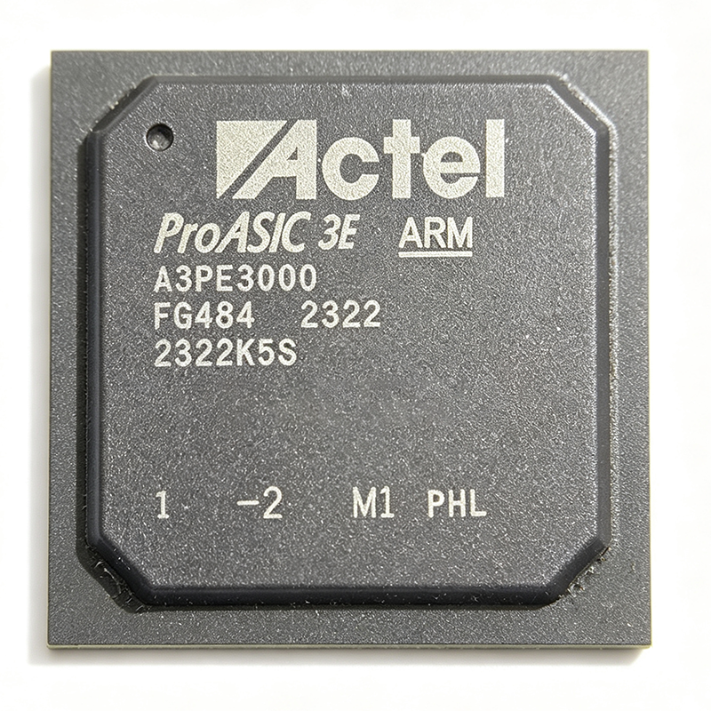
The Microchip Technology A3PE3000-1FGG484 is a 3-million-gate ProASIC3E flash-based FPGA with 75,264 logic elements, 341 user I/O, and 516,096 bits of embedded memory, housed in a 484-ball Fine-Pitch Ball Grid Array (FBGA) measuring 23 x 23 mm with a 1 mm ball pitch. The -1 speed grade device operates from a 1.5V core supply and supports system performance up to 231 MHz on the 130nm flash process. A flash FPGA is a field-programmable gate array whose configuration is stored in on-chip non-volatile flash memory rather than an external configuration device. Within the programmable logic hierarchy, the ProASIC3E family sits above smaller ProASIC3 parts and is positioned as a single-chip, low-total-cost-of-ownership solution: because the bitstream is stored on-chip, no external flash boot device is required, and the FPGA is inherently secure against bitstream interception. Key features of the A3PE3000-1FGG484 include instant-on power-up (the fabric is active within microseconds of power application), reprogrammability without a microprocessor, low dynamic power from the 1.5V core, and an abundance of advanced features typical of the ProASIC3E family, including embedded memory blocks and support for the Cortex-M1 soft processor in related M1 ProASIC3 variants. The 341 available user I/O support multiple single-ended and differential standards for flexible board-level integration. Architecturally, the device uses Microchip (formerly Actel/Microsemi) 130nm flash technology with a fine-grained fabric of versatile logic elements, routing resources, and distributed embedded flash memory totaling 516,096 bits. The 484-ball FBGA with 1 mm pitch balances I/O density with solderability on standard PCB assembly lines. Typical applications include industrial automation and motor control, aerospace and defense systems requiring non-volatile, secure configuration, medical instrumentation, and communications equipment where single-chip instant-on logic replaces CPLD-plus-FPGA two-chip solutions. When designing with this device, confirm the industrial temperature variant (A3PE3000-1FGG484I) if the end environment exceeds commercial ranges, and budget power distribution for the 1.5V core rail. Pricing on distributor channels is roughly $1,782 per unit for the industrial variant as of 2026-09-02. This page synthesizes distributor pricing, same-footprint drop-in alternatives across the ProASIC3E and ProASIC3L families, and practical design notes not found in the manufacturer datasheet.
A3PE3000-1FGG484I - Flash FPGA, 3M Gates | Microchip Technology
The Microchip Technology A3PE3000-1FGG484I is a ProASIC3E flash-based FPGA with 3,000,000 system gates, 35,000 logic elements, 504 Kbits of true dual-port SRAM, and 341 user I/O, delivered in a 484-ball FBGA package with 1.0 mm pitch. This industrial-temperature variant is a single-chip, reprogrammable logic device that powers up immediately from its nonvolatile flash configuration. A field-programmable gate array (FPGA) is a semiconductor device whose logic fabric is configured by the designer after manufacturing rather than being fixed at the foundry. FPGAs implement parallel hardware data paths using configurable logic blocks, embedded memory, and programmable routing. ProASIC3E belongs to the flash-based FPGA hypernym, which contrasts with SRAM-based FPGAs that require external configuration memory. Because the configuration is stored in flash cells, the A3PE3000-1FGG484I is live at power-up and offers higher security against readback, simplifying system design and reducing bill-of-materials cost. Key features include a 130-nm, seven-layer-metal (six copper) CMOS process, 1.5 V core supply, system performance up to 231 MHz, and up to 616 user I/O across the family. The 504 Kbit true dual-port SRAM supports simultaneous read/write for FIFOs and multi-clock domain buffering. Flash-based security features and the green FGG finish support lead-free assembly while making the configuration nonvolatile and more resistant to unauthorized readback. Architecturally, the device implements Microsemi/Microchip VersaTile logic elements surrounded by embedded SRAM blocks and programmable I/O. The flash switch fabric is configured in-system via JTAG using Microchip's FlashPro programmer. Since configuration memory is nonvolatile, no boot flash or FPGA configuration controller is required. The part also supports optional soft ARM processor cores for SoC-style designs, per the ProASIC3E datasheet description. Typical applications include industrial motor control, communications line cards, video capture/processing, medical equipment, automotive infotainment, and aerospace interfaces where low cost, low power, and secure flash configuration are needed. With 341 user I/O, it can interface to parallel ADC/DACs, SDRAM controllers, Ethernet PHYs, and custom backplanes. When designing, provide a clean 1.5 V core supply with adequate decoupling at the many VCC balls, and use Microchip Libero SoC software for timing closure and power estimation. For FGG484, thermal relief and ground plane design are important because the BGA has no exposed pad; route the 1.0 mm pitch with microvias or fine trace widths. This page combines distributor-verified pricing, drop-in FBGA-484 alternatives, package diagrams, and practical design notes not printed in the manufacturer datasheet, helping engineers make faster, more confident replacement and procurement decisions.
A3PE3000-1FGG896 - ProASIC3E Flash FPGA 3M Gates 620 I/O | Microchip
The Microchip Technology A3PE3000-1FGG896 is a ProASIC3E flash-based FPGA featuring 3,000,000 system gates, 75,264 logic cells, and 620 user I/Os, housed in an 896-ball Fine-Pitch Ball Grid Array (FBGA) package at speed grade -1. A flash FPGA is a field-programmable gate array whose configuration is stored in on-chip nonvolatile flash memory rather than an external configuration device. Within the programmable logic hierarchy, the A3PE3000-1FGG896 sits as a system-gate-class device under the broader FPGA and programmable logic category, part of Microchip (formerly Actel/Microsemi) ProASIC3E third-generation flash family that succeeded the ProASICPLUS family. Key features include single-chip, Instant-On operation enabled by nonvolatile flash technology, reprogrammability without external boot flash, low total cost of ownership (TOC), and ASIC-level unit cost at volume. The flash fabric removes the configuration-time and security concerns of SRAM FPGAs, since the bitstream is stored on-chip and does not need to be loaded at power-up. The ProASIC3E architecture provides high-performance logic fabric with embedded block memory for data buffering and system integration, supporting complex digital designs that previously required an ASIC or an SRAM FPGA plus configuration device. The 896-ball FGG package provides the highest I/O count option in the family, making the 620 available user I/Os suitable for wide bus interfaces and high-pin-count system interconnect. Typical applications include industrial automation and control, communications and networking equipment, medical instrumentation, aerospace and defense systems, and ASIC prototyping where the flash fabric's security and single-chip operation provide system-level benefits. A key design consideration is that the -1 speed grade is the slowest grade in the family; if timing closure is difficult, the -2 grade in the same 896-ball package (A3PE3000-2FGG896) is a same-footprint option. Verify I/O banking rules and power sequencing in the manufacturer datasheet before board layout. This page synthesizes distributor availability, same-package drop-in alternatives, and practical design notes not found in the manufacturer datasheet.
A3PE3000-1FGG896I - ProASIC3E Flash FPGA 3M Gates | Microchip
The Microchip Technology A3PE3000-1FGG896I is a ProASIC3E flash-based FPGA delivering 3,000,000 system gates, 75,264 logic cells, 620 user I/Os, and 516,096 bits of embedded RAM, operating at up to 272 MHz from a 1.5 V core supply (1.425 V to 1.575 V) in an 896-ball Fine-Pitch Ball Grid Array (FBGA) package with industrial temperature grading. A flash-based FPGA is a field-programmable gate array whose configuration data is stored in on-chip flash memory rather than an external configuration ROM. Within the programmable logic hierarchy, the A3PE3000-1FGG896I sits in the high-density tier of the ProASIC3E family, which belongs to the broader class of nonvolatile FPGAs and programmable system-on-chip platforms. Because the configuration is retained in flash, the device powers up instantly as a single-chip solution with no external boot device. Key differentiating features include low total cost of ownership through single-chip integration, reprogrammability in-system, support for high-performance system-level designs, and abundant advanced features beyond the earlier ProASICPLUS generation. The 620 I/O count and 516 Kbit RAM make it suited to wide-bus interfaces and data buffering. Architecturally, the device is built on a 130 nm CMOS flash process with a sea-of-modules fabric, distributed SRAM/FIFO blocks, and flexible I/O banking. The -1 speed grade supports core toggling rates up to 272 MHz, sufficient for pipelined DSP datapaths, protocol engines, and glueless processor interfacing. Typical applications include industrial automation controllers, communications and networking line cards, medical instrumentation, aerospace/defense systems requiring single-chip instant-on logic, and test equipment where 620 I/Os terminate backplanes and sensor arrays. A key design consideration: flash FPGAs trade some raw fabric speed versus the fastest SRAM FPGAs, so verify timing closure at 272 MHz with Microchip Libero SoC before committing the PCB. Plan power distribution for the 1.5 V core rail across the 896-ball array. This page synthesizes distributor pricing, same-footprint drop-in speed-grade and low-power alternatives, and practical design notes not found in the manufacturer datasheet.
A3PE3000-1PQG208I - ProASIC3E FPGA 3M Gates | Microchip
The Microchip Technology A3PE3000-1PQG208I is a ProASIC3E flash-based Field Programmable Gate Array (FPGA) with 3 million system gates, 147 user I/Os, and 516,096 bits of true dual-port SRAM, housed in a 208-pin PQFP (BFQFP) package. It operates from a 1.5V core supply and supports a system performance of up to 272 MHz, making it a single-chip, live-at-power-up solution for mid-density logic integration. An FPGA (Field Programmable Gate Array) is an integrated circuit that can be configured by the customer after manufacturing to implement arbitrary digital logic functions. Unlike ASICs, FPGAs are reprogrammable, allowing design changes without re-fabrication. The ProASIC3E family uses a flash-based configuration cell, which retains the design even when power is removed, eliminating the need for external boot memory and providing instant-on operation. This places the A3PE3000 within the hierarchy: FPGA -> flash FPGA -> ProASIC3E family -> mid-density programmable logic -> semiconductor. Key features include 3 million system gates, 147 user I/Os, 516,096 bits of true dual-port SRAM, and a 130-nm, 7-layer metal (6 copper) flash-based CMOS process. The device supports live-at-power-up operation, meaning it is ready to function immediately upon power application, and offers Level 0 support for secure in-system programming. The 208-pin PQFP package provides a compact footprint for board-level integration while maintaining adequate I/O count for moderate complexity designs. Technically, the ProASIC3E architecture uses a VersaTile core that can be configured as either a three-input lookup table (LUT) or a D-flip-flop/latch with enable, enabling efficient use of the FPGA fabric. The flash-based configuration is non-volatile, providing inherent security against reverse engineering and eliminating the need for configuration PROMs. The device supports 1.5V core operation with 3.3V, 2.5V, and 1.8V I/O standards, offering flexibility in mixed-voltage systems. Typical applications include industrial control, communications infrastructure, automotive electronics, and aerospace systems where reliability, instant-on capability, and security are critical. The 147 user I/Os and 3M gates are well-suited for glue logic, bus interfacing, and moderate digital signal processing tasks. The flash-based architecture is particularly valuable in safety-critical applications requiring deterministic startup behavior. When designing with this device, ensure adequate decoupling on the 1.5V core supply and all I/O banks. The PQFP package requires careful thermal management; a thermal pad or airflow may be necessary for high-utilization designs. Refer to the ProASIC3E datasheet for specific power supply sequencing and programming voltage requirements. This page synthesizes distributor pricing, drop-in alternatives, and practical design notes not found in the manufacturer datasheet, providing engineers with a comprehensive resource for evaluating the A3PE3000-1PQG208I in their designs.
A3PE3000-2FG324 - ProASIC3E FPGA 3M Gates 324-BGA | Microchip
The Microchip Technology (Microsemi) A3PE3000-2FG324 is a ProASIC3E flash-based FPGA with 3 million system gates (35,000 logic elements), 221 user I/Os, and a system performance rating of 310 MHz, fabricated on a 130 nm flash process and housed in a 324-ball FBGA package measuring 19 x 19 mm. An FPGA (Field-Programmable Gate Array) is a semiconductor device containing a fabric of configurable logic blocks, routing resources, and I/O cells that designers program to implement custom digital circuits. Unlike SRAM-based FPGAs, flash-based FPGAs such as the ProASIC3E family store their configuration in on-chip flash cells, giving them instant-on, single-chip operation without an external boot configuration device and inherent protection against bitstream readback. Key features of the A3PE3000-2FG324 include reprogrammable flash configuration, a 1.5 V core supply with a tolerance window of 1.425 V to 1.575 V, low total cost of ownership as an ASIC replacement, and support for soft-processor implementations including the 32-bit ARM Cortex-M1 on M1 ProASIC3 family variants. The 324-FBGA surface-mount package provides a compact footprint for space-constrained designs. Architecturally, the ProASIC3E fabric uses VersaTiles - fine-grained logic tiles based on a 130 nm flash switching element - delivering deterministic performance of up to 310 MHz system speed. Embedded block SRAM and abundant routing resources support data-path, communications, and control applications. Typical applications include consumer electronics, networking and communications equipment, computing platforms, industrial control, and avionics systems where a cost-effective ASIC replacement with reprogrammability is required. A key design consideration is the supply voltage tolerance: the 1.425 V to 1.575 V window demands a tightly regulated 1.5 V rail, and the 0 C to +85 C junction operating range should be verified against your thermal budget since this commercial-grade part is not automotive qualified. This page synthesizes distributor pricing, drop-in alternatives, and practical design notes not found in the manufacturer datasheet, verified against distributor listings as of 2026-09-02.
A3PE3000-2FG324I - ProASIC3E Flash FPGA 35K LEs | Microchip
The Microchip Technology (Microsemi) A3PE3000-2FG324I is a ProASIC3E family flash-based FPGA with 3 million system gates, 35,000 logic elements (LEs), 221 user I/Os, and a system performance rating of 310 MHz, housed in a 324-ball Fine-Pitch Ball Grid Array (FBGA) package and fabricated on a 130 nm flash process with a 1.5V core supply. A flash-based FPGA is a field-programmable gate array that stores its configuration in on-chip non-volatile flash memory rather than an external configuration ROM. In the programmable logic hierarchy - programmable logic device (PLD) to FPGA to system-on-chip - flash FPGAs occupy the single-chip niche: they power up instantly, require no boot device, and resist radiation-induced configuration upset better than SRAM FPGAs. Key features of the A3PE3000-2FG324I include single-chip operation with no external configuration memory, low total cost of ownership (TOC), reprogrammability, and industrial temperature operation from -40C to +85C. The speed grade 2 rating delivers up to 310 MHz system performance, and the 221 available I/Os support a broad set of single-ended and differential standards. Technically, the ProASIC3E fabric is built from versatile logic elements on Microsemi's (now Microchip's) 130 nm flash process. The non-volatile flash switch architecture eliminates configuration loading time, reduces bill-of-materials cost, and improves board-level security because the bitstream is never exposed on an external bus. Embedded block RAM, PLL support, and optional soft ARM Cortex-M1 capability (in related M1 ProASIC3 devices) make the family suitable for system-level integration. Typical applications include industrial automation controllers, aerospace and defense subsystems, medical instrumentation, and communications bridge logic, where instant-on operation, single-chip configuration, and long product lifecycle are essential requirements. When designing with this device, plan power distribution around the 1.5V core rail and verify I/O bank voltage assignments early in the pin-planning stage; Libero SoC design software provides pin-report checks before layout freeze. This page synthesizes distributor pricing, drop-in same-footprint alternatives across speed grades and temperature ranges, and practical design notes not found in the manufacturer datasheet.
A3PE3000-2FG484 - 3M-Gate ProASIC3E Flash FPGA | Microchip
The Microchip (Microsemi/Actel) A3PE3000-2FG484 is a 3-million-gate ProASIC3E flash-based FPGA with 75,264 logic cells, 341 user I/Os, and 516,096 bits of embedded SRAM, housed in a 484-ball FBGA (FG484) package operating at a 1.5V core voltage on a 130nm flash process. A flash-based FPGA is a field-programmable gate array whose configuration is stored in on-chip non-volatile flash cells rather than the SRAM-based configuration used by Xilinx and Altera devices. Within the programmable logic hierarchy, this makes the ProASIC3E a single-chip, instant-on solution: no external boot flash is required, the device is live at power-up, and no configuration bitstream is exposed, which inherently improves system security and simplifies board design. Key features include the ProASIC3E fabric's VersaTile architecture, where each tile can be configured as a 3-input LUT, a D-flip-flop, or memory, giving extremely flexible logic placement. The -2 speed grade supports system performance up to approximately 310 MHz, and the embedded 516 Kbit SRAM supports dual-port operation for FIFOs and buffering. Optional soft ARM support (via Cortex-M1 soft core licensing) allows a complete system-on-chip integration on one die. Technical depth: the 130nm flash CMOS process yields low static power compared to SRAM FPGAs, and non-volatile configuration eliminates configuration-time sequencing failures. The FG484 package (0.8mm... ball-pitch PBGA, square) is footprint-compatible with FG256 per the datasheet, easing migration paths. Typical applications include industrial automation controllers, medical instrumentation, communications line cards, and military/aerospace single-chip designs where instant-on and high security matter. Design consideration: the commercial-grade (no I suffix) device is rated 0C to +85C; for -40C to +100C use the A3PE3000-2FG484I industrial variant, which shares the same package footprint. This page synthesizes distributor pricing, drop-in alternatives, and practical design notes not found in the manufacturer datasheet.
A3PE3000-2FG484I - ProASIC3E FPGA 3M Gates | Microchip
The Microchip Technology A3PE3000-2FG484I is a ProASIC3E flash-based Field Programmable Gate Array (FPGA) offering 3 million system gates, 310 MHz system performance, and 516,096 bits of RAM, housed in a 484-pin FBGA package. It operates from a 1.5V core supply and provides 341 user I/Os, making it a high-density, low-power solution for a wide range of applications. An FPGA (Field Programmable Gate Array) is an integrated circuit that can be configured by the customer after manufacturing to implement any digital logic function. Unlike ASICs, FPGAs are reprogrammable, allowing design changes without costly mask revisions. The ProASIC3E family uses flash-based configuration cells, which are non-volatile, meaning the device retains its configuration when power is removed, eliminating the need for external boot memory and providing instant-on capability. This makes it a secure, single-chip solution in the programmable logic hierarchy, positioned between CPLDs and high-end SRAM-based FPGAs. Key features of the A3PE3000-2FG484I include 3 million system gates, 75,264 logic cells (CLBs), 516,096 bits of embedded RAM, and 341 user I/Os. It supports up to 310 MHz system performance and is fabricated in 130nm flash technology. The device includes advanced features such as programmable I/O standards, clock conditioning circuits (CCC/PLL), and an abundance of routing resources. Its flash-based architecture provides inherent security against reverse engineering and configuration bitstream interception, a critical advantage over SRAM-based FPGAs. Technically, the ProASIC3E family integrates a flash switch fabric that is programmed at the factory or in the field. The device supports multiple I/O standards including LVCMOS, LVTTL, PCI, and differential standards like LVDS and LVPECL. It includes up to 6 PLLs and 6 CCCs for clock management. The 130nm process technology balances performance and power, with a core voltage of 1.5V and low static power consumption. The 484-pin FBGA package (23x23 mm, 1.0 mm pitch) provides excellent thermal and electrical characteristics for high-density designs. Typical applications include industrial automation, communications infrastructure, medical imaging, aerospace and defense systems, and consumer electronics. The device is ideal for implementing glue logic, bus interfaces, protocol controllers, and DSP functions. Its non-volatile, secure configuration makes it suitable for applications requiring high reliability and anti-tamper features, such as encryption engines and secure boot controllers. When designing with this FPGA, consider the power supply decoupling: place 0.1uF and 10uF capacitors close to each VCC and GND pin to minimize noise. Also, use the dedicated programming pins (TCK, TMS, TDI, TDO) for in-system programming via JTAG. The device supports both JTAG and SPI flash programming, allowing flexible configuration updates. This page synthesizes distributor pricing, drop-in alternatives, and practical design notes not found in the manufacturer datasheet, providing engineers with a comprehensive resource for evaluating the A3PE3000-2FG484I.
A3PE3000-2FG896 - ProASIC3E FPGA, 3M Gates, 620 I/O | Microchip
The Microchip Technology A3PE3000-2FG896 is a ProASIC3E flash-based FPGA delivering 3 million system gates with 620 user I/Os in an 896-ball FBGA (FG896) package, operating from a 1.5 V core supply at speed grade -2 and supporting system frequencies up to 310 MHz on 130 nm flash technology. A flash-based FPGA is a field-programmable gate array whose configuration is stored in on-chip non-volatile flash cells rather than volatile SRAM. This places the ProASIC3E family in the power-management-friendly middle of the programmable logic hierarchy: unlike SRAM FPGAs it needs no external configuration PROM, boots instantly at power-up, and offers inherently lower static power and higher SEU immunity, making it a single-chip solution for cost-sensitive and high-reliability designs. Key features include 516,096 bits of configuration capacity reported alongside 620 usable I/Os per DigiKey listing, reprogrammable flash fabric supporting secure in-system programming, and abundant advanced features noted by Microchip such as low total cost of ownership (TOC) and strong system performance. The non-volatile fabric eliminates the brown-out configuration risks typical of SRAM devices. Technically, the device is built on a 130 nm flash process with a 1.5 V core. The -2 speed grade balances performance and cost within the ProASIC3E family, which spans densities from 15K to 3M gates. I/O banks support a wide range of voltage-referenced standards, with one VREF pin required per minibank when using voltage-referenced I/O standards, per the ProASIC3E family datasheet (DS0098). Typical applications include industrial automation controllers, communications and networking line cards, aerospace and defense systems requiring instant-on operation, and medical equipment where configuration data must not be externally readable. Design consideration: confirm I/O bank voltage assignment early in PCB layout, since the 896-ball FBGA footprint fixes ball assignments and voltage-referenced standards require dedicated VREF pins per minibank. This page synthesizes distributor pricing, verified cross-references, and drop-in alternatives in the same FG896 footprint - information not consolidated in the manufacturer datasheet.
A3PE3000-2FG896I - ProASIC3E FPGA 3M Gates 620 I/O | Microchip
The Microchip Technology (formerly Actel/Microsemi) A3PE3000-2FG896I is a ProASIC3E flash-based FPGA with 3 million system gates, 75,264 logic cells, 516,096 bits of embedded RAM, and 620 user I/Os, housed in an 896-ball FBGA (31 x 31 mm, 1.0 mm ball pitch) package with an industrial temperature rating of -40C to +100C junction temperature. A flash-based FPGA is a field-programmable gate array whose configuration is stored in on-chip flash memory rather than an external configuration PROM. Within the programmable logic hierarchy - FPGA -> programmable logic device -> digital IC - flash FPGAs occupy a distinct niche: they power up instantly (single-chip solution), retain configuration through power cycles, and offer inherently higher security and lower static power than SRAM FPGAs, which must reload configuration from external memory at every boot. Key features of the A3PE3000 include its nonvolatile flash fabric on a 130nm process, single 1.5V core supply (1.425V to 1.575V operating range), speed grade -2 performance, and embedded SRAM blocks totaling 516,096 bits. Because configuration data lives in flash, no external boot device is required, reducing bill-of-materials cost and board area and improving resistance to bitstream interception - a frequent reason avionics and industrial designers choose ProASIC3E over SRAM-based rivals. Architecturally, the ProASIC3E fabric is built from VersaTiles (fine-grained logic modules) interconnected through a hierarchical routing structure, with embedded flash switches storing each routing configuration bit. The -2 speed grade supports system clock rates up to roughly 350 MHz per third-party listings, and the E variant adds embedded RAM blocks plus extensive I/O standards support for interfacing with memory buses and high-speed peripherals. Typical applications include avionics and military systems requiring secure, instant-on logic, industrial automation controllers, networking and communications line cards, medical equipment, and ASIC prototyping where the 3M-gate capacity accommodates substantial RTL designs. A critical design consideration: this specific ordering code is RoHS non-compliant (lead-bearing solder balls), so confirm regulatory requirements before design-in; the FGG (green) package variants are the RoHS-compliant equivalents in the same footprint. Verify supply voltage sequencing of the 1.5V core and 2.5V/3.3V I/O banks per the manufacturer datasheet. This page synthesizes distributor pricing tiers, drop-in alternatives within the ProASIC3E family, and practical design notes not consolidated in the manufacturer datasheet.
A3PE3000-2FGG324 - ProASIC3E FPGA 3M Gates 324-BGA | Microchip
The Microchip Technology (formerly Microsemi/Actel) A3PE3000-2FGG324 is a ProASIC3E family flash-based FPGA with 3 million system gates (approximately 75,264 logic cells), a maximum system performance of 310 MHz, fabricated on 130nm flash technology, operating from a 1.5V core supply, and housed in a 324-pin Fine-Pitch Ball Grid Array (FBGA) package measuring 19 x 19 mm with 1 mm ball pitch. An FPGA (Field-Programmable Gate Array) is a semiconductor device containing a fabric of configurable logic blocks, memory blocks, and interconnects that designers program after manufacturing. Unlike SRAM-based FPGAs, the ProASIC3E family uses flash cells for configuration, meaning it is single-chip, instantly-on at power-up, and inherently secure against configuration bitstream copying because no external configuration flash is required. Key features of the A3PE3000-2FGG324 include reprogrammable flash fabric supporting live design updates, embedded variable-width SRAM blocks for FIFO and dual-port memory implementations, advanced I/O supporting multiple single-ended and differential standards, and low total cost of ownership through elimination of external boot memory. The ProASIC3E family combines high performance with ultra-low-density-class cost structure and small-footprint packaging options. Technically, the device uses Actel's third-generation flash architecture at 130nm, with speed grade 2 delivering up to 310 MHz system performance. The fabric includes PLLs for clock management, multiple embedded memory arrays totaling dedicated SRAM, and I/O banks that support LVDS-class differential signaling for high-speed board-level interfaces. Typical applications include industrial automation and control, military and aerospace systems requiring secure instant-on logic, communications infrastructure, test and measurement equipment, and medical instrumentation where single-chip reprogrammability, configuration security, and reliable power-up behavior are required. When designing with this device, plan power sequencing for the 1.5V core and auxiliary I/O rails, and verify I/O bank voltage compatibility with the board interface standards chosen. Because the fabric is flash-based, configuration corruption from cold-boot radiation or bitstream loss does not apply, simplifying system reliability analysis. This page synthesizes distributor pricing tiers, verified drop-in alternatives, and engineering design notes not consolidated in the manufacturer datasheet, aiding selection and shortage-risk mitigation.
A3PE3000-2FGG324I - 3M-Gate ProASIC3E Flash FPGA | Microchip
The Microchip (Microsemi/Actel) A3PE3000-2FGG324I is a ProASIC3E flash-based FPGA delivering 3 million system gates with 221 usable I/Os, 516 kbit of embedded flash memory, and system performance up to 272-310 MHz, housed in a 324-ball FBGA (FGG324, 19x19 mm) industrial-grade package rated from -40C to +100C junction temperature with a 1.5V core supply (1.425V to 1.575V). An FPGA (Field-Programmable Gate Array) is a reprogrammable semiconductor device that implements digital logic through configurable logic blocks and programmable interconnect. The ProASIC3E family belongs to the flash-based FPGA category, distinct from SRAM FPGAs because configuration is stored in on-chip nonvolatile flash cells, removing the need for an external boot flash and improving single-chip security and instant-on behavior. Key features of the A3PE3000-2FGG324I include its flash-based single-chip architecture (low total cost of ownership, no configuration PROM), 221 user I/Os supporting single-ended and differential standards, embedded 516,096-bit flash memory, and reprogrammability with secure design storage. The -2 speed grade and industrial temperature range make it suitable for harsh-environment deployments. Technically, the device is fabricated in 130nm flash CMOS process technology with a 1.5V core. The ProASIC3E fabric combines VersaTiles (logic modules), embedded RAM blocks, and flash configuration cells, supporting the Cortex-M1 soft processor and typical FPGA design flows in Libero SoC. Typical applications include industrial automation and motor control, aerospace and defense subsystems, communications and networking line cards, and secure single-chip control logic where nonvolatile, tamper-resistant configuration is required. A key design consideration is power: the 1.425V-1.575V core rail must be tightly regulated, and the 324-ball BGA requires careful PCB fanout and a dedicated power/ground ball pattern for signal integrity. This page synthesizes verified distributor data, drop-in alternative cross-references, and practical design notes not found in the manufacturer datasheet.
A3PE3000-2FGG484 ProASIC3E FPGA 3M Gates FBGA | Microchip
The Microchip Technology A3PE3000-2FGG484 is a ProASIC3E flash-based FPGA delivering 3 million system gates, 75,264 logic elements, and 341 user I/Os in a 484-ball FBGA package with 1.0 mm ball pitch. It operates with a 1.5 V core supply and supports system performance up to 310 MHz, providing a low-power, single-chip programmable logic solution for mid-density designs. An FPGA (Field-Programmable Gate Array) is a semiconductor device whose logic fabric can be reconfigured after manufacturing. Unlike SRAM-based FPGAs, the ProASIC3E family uses flash-based configuration cells, so the device is live at power-up and does not require an external boot memory. This makes it a member of the flash FPGA category, often considered when designers need instant-on, secure configuration, and lower system cost. Key features include 516,096 total RAM bits, 341 user I/O, a -2 speed grade, 130nm technology, and flash-based single-chip operation. The device supports multiple I/O standards and includes programmable phase-locked loops (PLLs) and embedded memories. The FGG suffix indicates a green, lead-free 484-ball FBGA package, meeting RoHS requirements for modern manufacturing. Architecturally, the A3PE3000-2FGG484 is built on Microchip's ProASIC3E flash FPGA fabric. Configuration data is stored in flash cells, providing inherent design security and instant-on capability. The device features 75,264 logic elements arranged as VersaTiles, and 516,096 bits of RAM. With a 1.5V core voltage and low static power, it fits power-sensitive applications where SRAM FPGAs would require configuration overhead. Typical applications include communications infrastructure, industrial automation, medical imaging, aerospace and defense systems, and broadcast video equipment. In these systems, the FPGA implements protocol bridging, DSP pre-processing, and system control functions. The 3M gate density and 341 I/Os allow designers to replace multiple discrete logic devices with a single programmable part. A key design consideration is power supply decoupling: place a 10uF bulk capacitor and multiple 0.1uF ceramics close to VCORE and VPLL pins. Because the FGG package uses a 1.0mm ball pitch, careful PCB breakout with micro-vias is recommended. Use thermal vias on the ground balls to improve heat transfer. This page synthesizes distributor pricing, drop-in alternatives, and practical design notes that are not all present in the manufacturer datasheet, giving engineers a faster path from selection to layout.
A3PE3000-2FGG896 - 3M-Gate ProASIC3E Flash FPGA | Microchip
The Microchip Technology A3PE3000-2FGG896 is a ProASIC3E flash-based FPGA delivering 3,000,000 system gates with 620 user I/Os in an 896-ball Fine-Pitch Ball Grid Array (FBGA, 31x31 mm, 1.0 mm ball pitch) package. A flash-based FPGA stores its configuration in on-chip flash memory rather than SRAM, so the device configures instantly at power-up with no external boot PROM. Within the programmable logic hierarchy (FPGA -> programmable logic device -> semiconductor), flash FPGAs sit apart from SRAM FPGAs because they are single-chip, non-volatile, and inherently secure against bitstream interception - a key reason ProASIC3E is widely adopted as an ASIC replacement in avionics, networking, and industrial systems. Key features include a 1.5V core supply (1.425V to 1.575V operating range), support for optional soft ARM support per the ProASIC3E datasheet, and the speed-grade -2 performance bin. The device supports voltage-referenced I/O standards with one VREF pin assigned per I/O minibank. Architecturally, the ProASIC3E fabric uses VersTiles with abundant embedded SRAM and flash memory resources, fabricated in CMOS technology. Flash switching elements keep static power low and eliminate configuration time, giving deterministic single-chip startup that SRAM FPGAs cannot match without auxiliary configuration devices. Typical applications include avionics and defense systems requiring bitstream security, networking and communications line cards, industrial control backplanes, and consumer high-volume designs migrating from ASIC where NRE cost matters. A key design consideration: the FG256/FG484 packages are footprint-compatible, and the G suffix in FGG indicates RoHS-compliant construction, so footprint reuse across the ProASIC3E family simplifies migration between densities. This page synthesizes distributor pricing, drop-in family alternatives, and practical design notes not found in the manufacturer datasheet.