FPGA & CPLD
Products (6352)
A3PE3000-2FGG896I - 3M Gate ProASIC3E FPGA | Microchip
The Microchip Technology A3PE3000-2FGG896I is a ProASIC3E flash-based Field Programmable Gate Array (FPGA) with 3 million system gates, 620 user I/Os, and 516,096 bits of RAM, housed in a 896-ball FBGA (31x31 mm) package. It operates from a 1.5V core supply (1.425V to 1.575V) and supports industrial temperature range from -40°C to 100°C (TJ). An FPGA (Field Programmable Gate Array) is an integrated circuit that can be configured by the customer after manufacturing to implement arbitrary digital logic functions. FPGAs belong to the programmable logic device (PLD) family, which sits between ASICs and microprocessors in the digital design hierarchy. The ProASIC3E family uses flash-based configuration, meaning the device retains its programming without external boot memory, offering instant-on capability and enhanced security compared to SRAM-based FPGAs. Key features include 3 million system gates, 75,264 logic modules (VersaTiles), 620 user I/Os, and 516,096 bits of embedded RAM. The device supports system performance up to 310 MHz and is manufactured on a 130nm flash process. It offers low power consumption with a typical static power of 0.24W, making it suitable for power-sensitive applications. The flash-based architecture provides inherent security against reverse engineering and supports in-system programming (ISP) for field updates. The ProASIC3E architecture uses a proprietary VersaTile that can be configured as either a three-input lookup table (LUT) or a D-flip-flop/latch with enable, allowing efficient use of the FPGA fabric. This flexibility enables designers to implement both combinational and sequential logic efficiently. The device also includes dedicated phase-locked loops (PLLs) for clock management and supports various I/O standards including LVCMOS, LVTTL, PCI, and LVDS. Typical applications include industrial control systems, communications infrastructure, avionics, and consumer electronics. The flash-based nature makes it ideal for applications requiring secure boot, instant-on operation, and high reliability in harsh environments. The 896-ball FBGA package provides ample I/O for complex designs while maintaining a compact footprint. When designing with this device, consider the 1.5V core supply requirement and ensure adequate decoupling on all power pins. The device supports JTAG-based programming and can be configured via SPI or I2C interfaces. For high-speed designs, pay attention to the PLL configuration and I/O standard selection to meet timing requirements. This page synthesizes distributor pricing, drop-in alternatives, and practical design notes not found in the manufacturer datasheet, providing engineers with a comprehensive resource for evaluating the A3PE3000-2FGG896I.
A3PE3000-2PQG208 - ProASIC3E 3M-Gate Flash FPGA | Microchip
The Microsemi (now Microchip Technology) A3PE3000-2PQG208 is a ProASIC3E family flash-based FPGA delivering 3,000,000 system gates, 147 user I/Os, and 1.5V nominal core operation in a 208-pin fine-pitch BFQFP (PQG208, 0.5 mm pitch) gull-wing surface-mount package. The -2 speed grade supports system performance up to approximately 310 MHz. A flash FPGA is a field-programmable gate array whose configuration is stored in on-chip nonvolatile flash memory rather than an external configuration PROM. In the programmable logic hierarchy (FPGA -> programmable logic device -> programmable semiconductor), flash FPGAs occupy a distinct niche: they are Instant On at power-up, single-chip (no boot device), inherently more secure against bitstream interception than SRAM FPGAs, and reprogrammable in-system. Key features include nonvolatile ProASIC3E flash architecture on a 130 nm CMOS process, 516096 bits of embedded resources per the device coding, and low total cost of ownership through elimination of external configuration memory. The ProASIC3E family is positioned by Microchip as a cost-effective ASIC replacement for consumer, networking/communications, computing, and avionics markets, offering ASIC-level unit cost with FPGA time-to-market benefits. Technically, the A3PE3000 fabric combines VersTile logic elements with embedded block RAM, supporting the high-performance 32-bit Cortex-M1 soft processor on M1 variants of the same family. The 1.5V core (1.425V to 1.575V range) with commercial 0C to +70C temperature grading suits cost-driven, thermally controlled environments. Typical applications include industrial control, communications line cards, avionics interface glue logic, and ASIC prototyping where single-chip instant-on configuration matters. Design consideration: the 208-pin QFP with 0.5 mm pitch requires careful PCB land-pattern design and a reflow-compatible GND/VCC decoupling strategy; do not confuse the commercial (no suffix) part with the industrial -I suffix variant. This page synthesizes distributor availability, drop-in same-package alternatives, and practical design notes not found in the manufacturer datasheet.
A3PE3000-2PQG208I - 3M-Gate Flash FPGA, 147 I/O | Microchip
The Microchip Technology (Microsemi) A3PE3000-2PQG208I is a ProASIC3E family flash-based FPGA delivering 3 million system gates, 147 user I/Os, and a maximum system performance of 310 MHz, housed in a 208-pin fine-pitch PQFP (208-BFQFP / PQG208) package with gull-wing leads and an industrial temperature rating of -40C to +85C. An FPGA (Field-Programmable Gate Array) is a semiconductor device containing a fabric of configurable logic blocks, routing resources, and I/O cells that designers program to implement custom digital circuits. Within the hierarchy of programmable logic, the A3PE3000 belongs to the flash-based FPGA class - distinct from SRAM FPGAs - because configuration data is stored in on-chip flash memory, giving it inherent single-chip, non-volatile, instant-on behavior without an external configuration PROM. Key features include a 1.5V core supply typical of 130nm CMOS process technology, live-at-power-up (LAPU) operation enabled by flash storage, and reprogrammability that lowers total cost of ownership by eliminating external boot devices. The ProASIC3E family is positioned by Microchip as a cost-effective ASIC replacement for consumer, networking/communications, computing, and avionics markets. Technically, the device uses Microsemi's proprietary flash switch technology combining a flash cell and routing switch in a single unit, which reduces area and improves security versus SRAM-based competitors. Speed grade -2 denotes the faster commercial speed bin, supporting system clock rates up to 310 MHz per distributor data. Embedded features include support for the Cortex-M1 soft processor in the related M1 ProASIC3 variants, plus on-chip PLLs and RAM blocks typical of the ProASIC3E architecture. Typical applications include industrial control and automation, networking and communications line cards, avionics glue logic and interface bridging, medical instrumentation, and secure single-chip ASIC prototyping where non-volatile, tamper-resistant configuration matters. When designing with this device, remember that the 208-pin PQFP has higher lead inductance than BGA alternatives such as the FGG484, which can limit very high-speed I/O signaling; verify signal-integrity margins for edges faster than approximately 500 ps. This page synthesizes distributor pricing, drop-in alternatives, and practical design notes not found in the manufacturer datasheet, making it a one-stop reference for engineers evaluating the A3PE3000-2PQG208I.
A3PE3000-FG324 - ProASIC3E FPGA 3M Gates 324-BGA | Microchip
The Microchip (Microsemi) A3PE3000-FG324 is a ProASIC3E family flash-based FPGA delivering 3 million system gates with up to 221 user I/Os in a 324-ball FBGA package operating from a 1.5V core supply at system performance up to 231 MHz on 130nm flash technology. A field-programmable gate array (FPGA) is a semiconductor device containing configurable logic blocks (CLBs) and programmable interconnects that designers configure in the field after manufacturing. The ProASIC3E family sits within the broader hierarchy of programmable logic: FPGA -> programmable logic device -> digital logic IC -> semiconductor. Unlike SRAM-based FPGAs, ProASIC3E devices use flash cells for configuration, so they are single-chip, non-volatile solutions that boot instantly without an external configuration PROM. Key features include low total cost of ownership (TOC) through single-chip operation, in-system programmability (ISP), 128-bit AES decryption via JTAG (IEEE 1532-compliant), and FlashLock security designed to protect FPGA contents. The flash fabric also offers inherent resistance to configuration upset, important in avionics and industrial environments. Technically, the device provides 75,264 CLBs on a 130nm CMOS process, supporting high-performance 32-bit soft CPU implementations, and the ProASIC3E family adds embedded memory and enhanced I/O structures targeted at ASIC-replacement designs in consumer, networking/communications, computing, and avionics markets, per the Microchip ProASIC3E Flash Family FPGAs datasheet. Typical applications include ASIC replacement and prototyping, network and communications line cards, industrial control, and avionics subsystems where reprogrammability and single-chip boot matter. A key design consideration: the standard commercial grade A3PE3000-FG324 is listed by some datasheet aggregators as containing lead (RoHS non-compliant); the lead-free FGG variant (A3PE3000-FGG324) should be chosen where RoHS compliance is required. This page synthesizes distributor pricing, drop-in alternatives, FAQs, and design notes not found in the manufacturer datasheet.
A3PE3000-FG324I - ProASIC3E FPGA 3M Gates 324-BGA | Microchip
The Microchip Technology A3PE3000-FG324I is a ProASIC3E family flash-based FPGA delivering approximately 3 million system gates (35K logic elements per distributor listings) with 221 user I/Os, 231 MHz system performance, and a 1.5V core, housed in a 324-ball Fine-Pitch Ball Grid Array (FBGA) package with industrial temperature rating of -40C to +125C. A flash-based FPGA is a field-programmable gate array whose configuration is stored in on-chip flash memory cells rather than SRAM, so it powers up instantly without an external configuration PROM and is inherently single-chip. Within the programmable logic hierarchy, the A3PE3000 sits in the mid-density range of the ProASIC3/ProASIC3E family, which is part of the broader FPGA -> programmable logic -> semiconductor taxonomy from Microsemi (now Microchip Technology). Key features include nonvolatile flash programming that eliminates boot-time configuration and improves secure operation, support for high-performance 32-bit soft processors, low total cost of ownership through single-chip integration, and reprogrammability in-system. The 324-ball FBGA footprint with 221 available user I/Os provides substantial interface density for a mid-density device. Technically, the device is manufactured on a 130nm flash process operating from a 1.5V core supply. The ProASIC3E architecture combines VersTiles logic elements with embedded block RAM and abundant advanced features such as on-chip PLLs and I/O standards support for common single-ended and differential signaling, enabling glue logic consolidation, bus bridging, and control-plane designs. Typical applications include industrial automation control, communications and networking line cards, aerospace and defense subsystems requiring instant-on operation, and secure single-chip designs where external boot flash is undesirable. The industrial grade I suffix targets extended-temperature environments. When designing with this device, verify power sequencing and supply rail design against the manufacturer datasheet, and use Libero SoC design software for synthesis and place-and-route. This page synthesizes verified distributor data, drop-in alternatives from the same ProASIC3E family, and practical design guidance not consolidated on the manufacturer page.
A3PE3000-FG484 - ProASIC3E 3M-Gate Flash FPGA 484-BGA | Microchip
The Microchip Technology A3PE3000-FG484 is a ProASIC3E family flash-based FPGA delivering 3 million system gates (75,264 cells) with 341 user I/Os in a 484-ball Fine-Pitch Ball Grid Array (FBGA) package operating from a 1.5V core voltage at up to 231 MHz system performance. A flash-based FPGA stores its configuration in on-chip flash memory rather than the SRAM cells used by Xilinx and Intel (Altera) FPGAs. This means the A3PE3000-FG484 is a single-chip, non-volatile, instant-on solution: no external configuration PROM, no boot time, and inherent resistance to configuration readback attacks. Within the power-management hierarchy of programmable logic, flash FPGAs occupy the secure, low-total-cost-of-ownership niche between ASICs and SRAM FPGAs. Key features include reprogrammable flash fabric on a 130nm process, support for soft ARM processors via the CoreConsole/Libero design flow, single-chip operation that lowers bill-of-materials cost, and abundant advanced I/O standards including LVDS and LVPECL differential signaling. The FG484 package measures 23 x 23 mm with a 1.0 mm ball pitch and 2.23 mm height, and the FG256 and FG484 packages are footprint-compatible, providing an upgrade path within the family. Architecturally, the ProASIC3E fabric combines versatile logic elements, embedded block RAM, and flash configuration cells, with optional ARM soft-core support for embedded control applications. The fabric's non-volatile nature also reduces system power during standby because no configuration load cycle is needed at power-up. Typical applications include ASIC replacement in consumer electronics, networking and communications equipment, industrial computing, and avionics systems, where single-chip secure configuration and moderate gate density are valued. When designing with this part, budget for bank-based VCCI voltages: multiple I/O banks allow mixed-voltage signaling, but voltage-referenced standards require one VREF pin per minibank. This page synthesizes distributor pricing, drop-in alternatives across the ProASIC3/ProASIC3L families, and practical design notes not found in the manufacturer datasheet.
A3PE3000-FG484I - ProASIC3E FPGA 35K LE 341 I/O | Microchip
The Microchip Technology (Microsemi) A3PE3000-FG484I is a ProASIC3E flash-based FPGA with 3 million system gates, 35K logic elements (LEs), 341 user I/Os, and 504 Kbit (516096-bit) fabric RAM, housed in a 484-ball Fine-pitch Ball Grid Array (FBGA) package rated for -40C to +100C junction temperature. An FPGA (Field-Programmable Gate Array) is a reprogrammable semiconductor device that implements digital logic through configurable logic blocks and programmable interconnect. Within the power-management hierarchy of a system, the ProASIC3E family occupies the mid-density, nonvolatile flash FPGA tier: it sits between CPLDs and high-end SRAM FPGAs, offering single-chip operation because configuration data is stored in on-chip flash rather than an external boot flash. Key features of the A3PE3000-FG484I include instant-on, single-chip operation enabled by the flash fabric, a 1.5V core supply (1.425V to 1.575V operating range), support for optional soft ARM processor integration, and high I/O count (341) suited to wide bus interfaces. The ProASIC3E fabric also integrates embedded memory blocks totaling 516096 bits plus 1 Kbit of flash-based uPROM for secure version storage. Technically, the device is built on a 130nm flash process with a system performance rating up to 231 MHz. Unlike SRAM FPGAs, no configuration PROM or power-up configuration sequence is required, improving board-level reliability and reducing bill-of-materials cost. Flash cells also resist single-event configuration upsets better than SRAM, which benefits industrial and communications equipment. Typical applications include industrial automation control, communications and networking line cards, medical instrumentation, and aerospace/defense payloads where instant-on and nonvolatile configuration matter. The 484-ball package balances I/O density with moderate thermal and assembly requirements. When designing with this FPGA, power the 1.5V core and I/O banks in the sequence specified by the manufacturer datasheet and decouple each bank with low-ESR ceramics; the FBGA package requires careful via fan-out planning in the PCB layout stage. This page synthesizes distributor pricing, same-brand drop-in alternatives, and practical design notes not found in the manufacturer datasheet, providing a one-stop reference for procurement and engineering evaluation.
A3PE3000-FG896 - ProASIC3E Flash FPGA 620 I/O | Microchip
The Microchip Technology (Actel) A3PE3000-FG896 is a ProASIC3E flash-based FPGA with 3 million system gates, 620 user I/Os, and 231 MHz system performance, fabricated on a 130 nm flash process and housed in an 896-ball FBGA package with a 1.5 V core supply. A flash-based FPGA is a field-programmable gate array that stores its configuration in on-chip non-volatile flash memory cells rather than in an external configuration ROM, as SRAM FPGAs require. Within the power-management hierarchy of programmable logic, flash FPGAs sit between one-time-programmable antifuse devices and reprogrammable SRAM devices, offering single-chip, instant-on behavior with reprogrammability. The ProASIC3E family extends the ProASIC3 architecture with embedded SRAM and PCIe-ready I/O for system-level integration. Key features of the A3PE3000-FG896 include non-volatile flash configuration enabling a true single-chip solution with no external boot device, 620 user I/Os supporting a broad range of voltage-referenced and single-ended standards, and embedded memory totaling 516096 bits for FIFOs and dual-port buffering. The VersaTile architecture allows each tile to function as a three-input LUT, a D flip-flop, or a latch with enable, maximizing fabric efficiency. Technically, the device uses Microchip's third-generation flash switch technology on a 130 nm process. The fabric achieves a typical system clock rate of 231 MHz, and VersaNet global networks distribute low-skew, high-fanout clocks and resets across the die. The 896-ball FBGA provides abundant I/O and power/ground balls for signal-integrity headroom in high-pin-count designs. Typical applications include industrial automation controllers, communications and networking line cards, medical instrumentation, aerospace/defense subsystems requiring instant-on logic, and test equipment, all of which benefit from the 3M-gate capacity and 620 I/O count. Designers should note the commercial 0 C to +70 C operating range of this FG896 speed-grade: industrial applications must select the FG896I variant instead. Voltage-referenced I/O standards require one VREF pin per minibank per the ProASIC3E datasheet. This page synthesizes distributor pricing, drop-in same-package alternatives, and practical design notes not found in the manufacturer datasheet, as of 2026-09-02.
A3PE3000-FG896I - ProASIC3E FPGA, 3M Gates, 896-BGA | Microchip
The Microchip Technology A3PE3000-FG896I is a ProASIC3E flash-based FPGA with 3 million system gates (35K logic elements per distributor listings), 620 user I/Os, and a maximum system performance of 231 MHz, housed in an 896-ball Fine-Pitch Ball Grid Array (FBGA/896-BGA) package measuring 31x31x2.44 mm, qualified for the industrial temperature range. A field-programmable gate array (FPGA) is a semiconductor device containing a fabric of programmable logic blocks and interconnects that designers configure in the field, sitting in the system hierarchy between fixed-function ASICs and general-purpose processors. The ProASIC3E family belongs to the flash-based FPGA category: unlike SRAM FPGAs, it stores its configuration in nonvolatile flash, so the device is single-chip, Instant On, and inherently more secure because no external configuration bitstream is exposed at power-up. Key features include nonvolatile flash programming that eliminates the boot PROM and configuration controller, a 1.5V core supply, 130 nm flash process technology, reprogrammability for design iteration, and abundant advanced features such as clock conditioning circuits and embedded block support. The 620 available user I/Os make the FG896 package well suited to wide-bus, high-pin-count designs such as backplane interfaces and memory controllers. Technically, the ProASIC3E fabric uses a sea-of-gates architecture of VersaTiles built on Actel/Microchip's third-generation flash FPGA technology, delivering ASIC-replacement logic density at near-ASIC unit cost. The high-performance fabric supports system speeds up to 231 MHz, adequate for communications, avionics, and computing glue-logic consolidation. Typical applications include networking and communications equipment, industrial automation, avionics subsystems, and secure single-chip ASIC replacement in consumer and computing platforms. Design consideration: budget the 1.5V core rail with adequate decoupling and plan ball-out fanout early, since the 896-ball array requires careful PCB escape routing. This page synthesizes distributor pricing, drop-in alternatives, and practical design notes not found in the manufacturer datasheet.
A3PE3000-FGG324 - ProASIC3E FPGA 3M Gates 221 I/O | Microchip
The Microchip Technology (formerly Microsemi/Actel) A3PE3000-FGG324 is a flash-based ProASIC3E family FPGA with 3 million system gates, 221 user I/O, and a core supply voltage of 1.425V to 1.575V, housed in a 324-ball Fine-Pitch Ball Grid Array (FBGA) package measuring 19 x 19 mm with 1.0 mm ball pitch. A Field Programmable Gate Array (FPGA) is a reprogrammable semiconductor device that implements user-defined digital logic through a fabric of configurable logic blocks, routing resources, and I/O cells. Within the programmable logic hierarchy, the FPGA sits at the top of the density range, above CPLDs and SPLDs, and serves as an ASIC replacement or prototyping platform in system-on-chip and embedded designs. The ProASIC3E distinguishes itself from SRAM-based FPGAs by using nonvolatile flash cells to store the configuration, requiring no external boot PROM. Key features include flash-based nonvolatile configuration (instant-on, single-chip solution), 130 nm flash process technology, system performance up to approximately 231 MHz as cited in cross-reference data, 516096 bits of embedded flash resources per distributor listings, and optional support for soft ARM processors, enabling low total cost of ownership (TOC) with reprogrammability. Technically, the ProASIC3E fabric uses a sea-of-gates architecture of versatile logic elements, supported by embedded SRAM blocks and phase-locked loops for clock management. Because configuration is stored in flash, the device is secure against bitstream capture and immune to configuration volatility at power-off, a differentiator versus SRAM FPGAs. Typical applications include industrial automation controllers, networking and communications equipment, computing platforms, avionics systems, and consumer electronics, where the ProASIC3E family is positioned by Microchip as a cost-effective ASIC replacement. Design consideration: the 1.5V core rail must be held within the tight 1.425V to 1.575V window; use a dedicated LDO or buck regulator with adequate decoupling near the ball field. This page synthesizes distributor pricing, drop-in alternatives, and practical design notes not found in the manufacturer datasheet.
A3PE3000-FGG324I - ProASIC3E FPGA 3M Gates 324-BGA | Microchip
The Microchip Technology (Actel/Microsemi) A3PE3000-FGG324I is a ProASIC3E family flash-based FPGA with 3 million system gates, 75264 CLBs, 221 user I/Os, and a maximum toggle rate of 350 MHz, housed in a 324-ball Fine-Pitch Ball Grid Array (FBGA/PBGA324) measuring 19 x 19 mm with 1.0 mm ball pitch. A Field Programmable Gate Array (FPGA) is a semiconductor device that implements user-defined digital logic through a configurable fabric of logic blocks, routing resources, and I/O cells. The ProASIC3E sits in the flash-FPGA branch of this hierarchy: unlike SRAM-based FPGAs, it stores its configuration in nonvolatile flash, making it a single-chip, Instant-On solution that needs no external configuration device. Key features include nonvolatile flash programming with reprogrammability, 1.5 V core operation on a 130 nm process, embedded memory, and low total cost of ownership (TOC) as a cost-effective ASIC replacement. The industrial temperature grade (-40 C to +125 C ambient, denoted by the I suffix) supports harsh-environment deployment. Technically, the device uses the ProASIC3EVersaTile architecture, where each versatile cell can be configured as combinational logic, a flip-flop, or small memory, giving designers fine-grained control. The fifth-generation flash switch technology provides security benefits because configuration data cannot be easily read back, which matters in avionics, networking, and consumer designs where IP protection is required. Typical applications include ASIC prototyping and bridging, industrial control, networking and communications line cards, avionics subsystems, and high-reliability consumer platforms. The 221 available user I/Os allow wide parallel bus interfaces and glueless connection to processors and memories. A key design consideration is power supply sequencing and decoupling: the 1.5 V core rail requires stable, low-ripple supplies, and the BGA-324 footprint demands careful via-fanout planning during PCB layout. This page synthesizes distributor pricing context, verified drop-in alternatives, and practical design notes that go beyond the raw specifications listed in the manufacturer datasheet.
A3PE3000-FGG484 - ProASIC3E FPGA 3M Gates 484-BGA | Microchip
The Microchip Technology A3PE3000-FGG484 is a ProASIC3E family flash-based FPGA delivering 3 million system gates (75264 cells) with 341 user I/Os in a 484-ball FBGA package measuring 23 x 23 mm with a 1 mm ball pitch. Fabricated on a 130 nm flash process and operating from a 1.5 V core supply, it supports system performance up to 231 MHz. A flash-based FPGA is a field-programmable gate array whose configuration is stored in on-chip non-volatile flash memory rather than an external configuration device. Within the programmable logic hierarchy - FPGA -> field-programmable gate array -> programmable SoC/programmable logic device - flash FPGAs occupy the single-chip niche: they power up instantly, require no boot PROM, and offer inherent security against configuration readback compared with SRAM FPGAs. Key features include non-volatile flash programming (single-chip solution, low total cost of ownership), reprogrammability for in-field updates, abundant advanced features such as embedded block RAM, and the large 341 I/O count that suits wide bus interfaces. The ProASIC3E variant adds up to 2 Mbit of embedded RAM and PLL support, targeting system-level integration. Technically, the fabric uses a sea-of-gates architecture with VersNet routing and flash switch elements, eliminating volatile configuration and its associated power-up glitch risk. The 130 nm CMOS process with 1.5 V core keeps static power moderate, while the FBGA-484 footprint provides dense, high-speed interconnect for DDR-class interfaces. Typical applications include industrial automation controllers, communications and networking line cards, medical instrumentation, military/aerospace secure systems, and test equipment, where instant-on operation and configuration security are valued. A key design consideration: ProASIC3E FGG484 parts are RoHS lead-free (FGG suffix), whereas FG484 variants are not - verify soldering compatibility before substitution. This page synthesizes distributor pricing, drop-in alternatives within the ProASIC3/3E family, and practical design notes not found in the manufacturer datasheet.
A3PE3000-FGG484I - ProASIC3E FPGA 3M Gates 484-FBGA | Microchip
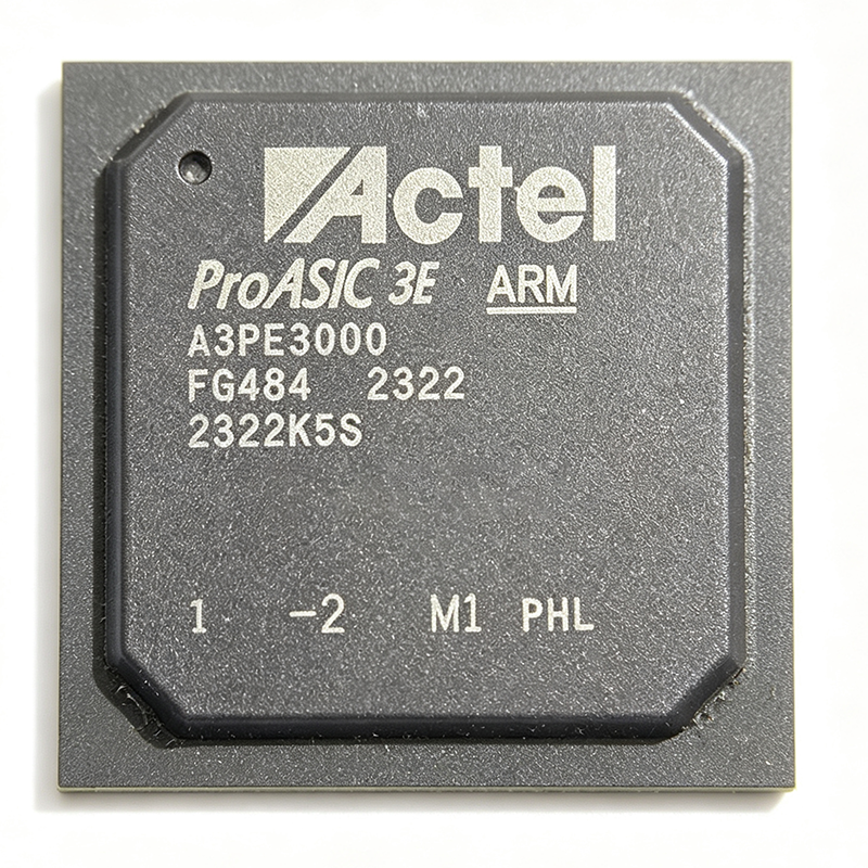
The Microchip Technology (Microsemi) A3PE3000-FGG484I is a ProASIC3E flash-based FPGA delivering 3 million system gates (75,264 logic cells), 341 user I/Os, and up to 516,096 bits of embedded RAM in a 484-ball Fine-Pitch Ball Grid Array (FBGA) package, rated for the industrial temperature range of -40C to +100C. A field-programmable gate array (FPGA) is a semiconductor device containing a fabric of programmable logic blocks and interconnects that designers configure in the field. The ProASIC3E family sits in the flash-based FPGA hierarchy: FPGA -> programmable logic device -> programmable SoC/system logic, distinguished from SRAM FPGAs by its nonvolatile flash configuration cells. Key features include flash-based live-at-power-up operation with no external configuration device, single 1.5V core operation on 130nm flash technology, low total cost of ownership through single-chip integration, and reprogrammability without a boot PROM. The 341 I/Os support multiple standards, and the 23x23 mm FBGA footprint suits high-IO industrial designs. Architecturally, the A3PE3000 uses a sea-of-vanilla logic tile fabric with Versatile routing, flash switch blocks, and embedded SRAM blocks totalling 516,096 bits. Because configuration is stored in flash, the device is inherently secure against bitstream interception and instantly active at power-up - critical for systems with fast-start requirements. Typical applications include industrial automation and motor control, aerospace and defense subsystems, medical instrumentation, communications bridging, and test equipment where nonvolatile, secure, instant-on programmable logic is required. A key design consideration: the FGG484I is the industrial-grade, RoHS-code-No variant in some parametric databases, so verify environmental compliance requirements against the official Microchip datasheet before finalizing BOM approvals. This page synthesizes distributor pricing signals, drop-in same-footprint alternatives, and practical design notes not found on the manufacturer product page alone.
A3PE3000-FGG896 - ProASIC3E 3M-Gate Flash FPGA 896-BGA | Microchip
The Microchip (Actel) A3PE3000-FGG896 is a ProASIC3E flash-based FPGA with 3 million system gates, 75264 CLBs, 620 user I/Os, and a maximum system performance of 231 MHz, housed in an 896-ball Fine-Pitch Ball Grid Array (FBGA) package operating from a 1.5V core supply. A flash-based FPGA is a field-programmable gate array whose configuration data is stored in on-chip flash memory cells rather than volatile SRAM. Unlike SRAM FPGAs, flash FPGAs retain their configuration through power cycles without an external configuration PROM, reducing bill-of-materials cost and improving system boot security. Within the power-management hierarchy of programmable logic devices, the FPGA sits above CPLDs and below full ASIC implementations, and the ProASIC3E family was positioned by Actel (now Microchip Technology) specifically as a cost-effective ASIC replacement for high-volume applications. Key differentiating features of the A3PE3000 include single-chip operation with no external boot device, reprogrammability with live-at-power-up behavior, low total cost of ownership, and abundant embedded block resources. The ProASIC3E fabric is built on a 130nm flash process technology, delivering deterministic, high-performance logic capacity of 35K logic elements with 516096 bits of distributed and block memory for buffering, FIFOs, and data-path functions. Architecturally, the device combines a sea-of-versatile-modules fabric with embedded flash switches, which supply inherent security benefits because configuration data is non-volatile and cannot be easily read back. This makes the family attractive for avionics, networking, computing, and consumer platforms where IP protection matters. The 620 available I/Os support broad system connectivity within a single 896-ball package. Typical applications include industrial control systems, wireless and networking communication equipment, ASIC prototyping and low-volume ASIC replacement, and avionics subsystems that require non-volatile, secure configuration storage. A key design consideration is supply integrity: the 1.5V core rail must be well-regulated and decoupled, and BGA escape routing requires careful fanout planning on high-layer-count PCBs. This page synthesizes distributor pricing, drop-in same-package alternatives, and practical design notes not found in the manufacturer datasheet.
A3PE3000-FGG896I - ProASIC3E FPGA 620 I/O | Microchip
The Microchip Technology (Microsemi) A3PE3000-FGG896I is a ProASIC3E Flash-based FPGA with 35,000 logic elements (LEs), 620 user I/Os, and system performance up to 231 MHz, housed in an 896-ball Fine-Pitch Ball Grid Array (FBGA/FGG896) package and rated for the industrial temperature range of -40C to +85C. It operates from a 1.5 V core supply and is fabricated on a 130 nm flash process. A Flash FPGA is a field-programmable gate array that stores its configuration in on-chip nonvolatile flash memory rather than an external configuration ROM. In the programmable logic hierarchy, the A3PE3000 sits within the ProASIC3E family, which itself belongs to the broader categories of nonvolatile FPGAs, programmable logic devices, and digital semiconductors. Because the configuration is retained on-chip, the device is a true single-chip, Instant-On solution that needs no boot PROM and offers inherent resistance to configuration readback. Key features include reprogrammable flash fabric based on the third-generation VersaTile architecture, where each tile functions as a three-input LUT or a D-flip-flop/latch with enable; a large 620-pin I/O budget supporting high-pin-count board interfaces; low total cost of ownership through single-chip integration; and industrial-grade temperature qualification for harsh environments. The ProASIC3E fabric provides distributed block routing and embedded memory within the family architecture, supporting glue logic consolidation, bus bridging, control-plane functions, and custom data-path implementations. The VersaTile structure allows efficient synthesis mapping, and Microchip's Libero SoC design suite supports HDL entry, synthesis, simulation, and programming of the device. Typical applications include industrial automation controllers, communications and networking line cards, test and measurement instrumentation, medical equipment, and aerospace/defense subsystems where nonvolatile, secure, single-chip FPGA integration is required. A key design consideration is power distribution: the 1.5 V core rail must be well regulated and decoupled across the 896-ball package, and high-speed I/O banks require careful banking and reference planning in the pinout assignment. This page synthesizes verified distributor data, drop-in same-family alternatives, and practical design notes not found in the manufacturer datasheet.
A3PE3000-PQ208I - 3M-Gate Flash FPGA 147 I/O | Microchip
The Microchip (Microsemi) A3PE3000-PQ208I is a flash-based FPGA from the ProASIC3E family with 3 million system gates, 75264 configurable logic cells, up to 231 MHz system performance, 147 user I/O, and 1.5V core operation on a 130nm process, housed in a 208-pin PQFP (28 x 28 mm, 0.5 mm pitch) package with industrial temperature rating. A field-programmable gate array (FPGA) is a semiconductor device containing a fabric of configurable logic blocks, routing resources, and programmable I/O that designers configure after manufacturing. Within the programmable logic hierarchy, the FPGA sits at the top as a full system-level fabric, above CPLDs and simple programmable devices. The ProASIC3E family is distinguished by its flash-based configuration memory: unlike SRAM FPGAs, it is a single-chip solution that retains its configuration through power cycles and needs no external boot PROM, reducing bill-of-materials cost and improving board-level security. Key features of the A3PE3000 include 3 million gates for substantial logic capacity, 147 user I/O on the PQ208 package, low total cost of ownership (TOC) highlighted by Microchip, and reprogrammability supporting in-field firmware updates. The flash cell technology is inherently non-volatile and low power at standby, and the fabric supports common FPGA design flows using Microchip Libero SoC tools. Technical depth: the device is fabricated on a 130nm CMOS process with a 1.5V core supply. ProASIC3E embeds PLLs and block RAM suitable for bus interfacing, glue logic consolidation, and control-plane designs. The 231 MHz figure represents the family's achievable system performance for typical pipelined designs. Clock management, I/O banking, and flash security features make the part a cost-effective ASIC replacement, particularly where NRE cost and long ASIC lead times are unacceptable. Typical applications include industrial automation control and motor-interface glue logic, networking and communications line-card control logic, and avionics/defense systems that value non-volatile, single-chip, secure configuration without external configuration devices. Design consideration: this PQ208I variant is RoHS non-compliant and contains lead, so it is targeted at legacy, defense, and exemption-qualified industrial programs; for new lead-free designs, select the PQG208 green-package variants instead. This page synthesizes distributor pricing, same-package drop-in alternatives, and practical design notes not found in the manufacturer datasheet, with pricing verified as of 2026-09-02.
A3PE3000-PQG208 - ProASIC3E 3M-Gate Flash FPGA, 208-PQFP | Microchip
The Microchip (formerly Microsemi/Actel) A3PE3000-PQG208 is a 3-million-gate ProASIC3E flash-based FPGA with 75264 CLBs, up to 516096 bits of embedded memory, a maximum toggle-frequency figure of 231 MHz, fabricated on a 130nm CMOS flash process with a 1.5V core, housed in a 208-pin PQFP (PQG208) package measuring 28 x 28 mm with 0.5 mm lead pitch. An FPGA (field-programmable gate array) is a semiconductor device containing a fabric of programmable logic blocks and interconnects that the user configures after manufacturing. The ProASIC3E family sits within the broader hierarchy of programmable logic devices: FPGA -> flash-based FPGA -> single-chip, non-volatile FPGA -> programmable SoC platform. Unlike SRAM FPGAs, ProASIC3E devices store their configuration in on-chip flash, so they power up instantly without an external configuration PROM and offer higher design security. Key features include the flash-based, single-chip architecture with low total cost of ownership (TOC), reprogrammability, support for the ARM Cortex-M1 32-bit soft processor, and abundant embedded RAM blocks. The PQ208 package supports six clock-conditioning circuits (CCCs) and two PLLs, with six chip-level (main) and three quadrant global clock networks available for low-skew clock distribution. Technically, the device uses a 130nm CMOS flash switching fabric with a 1.5V core supply, supporting multiple single-ended and differential I/O standards; certain I/O standard usage is limited on the A3PE3000 density, and each used differential I/O pair reduces the single-ended I/O count by two. The large 3M-gate capacity suits high-gate-count glueless integration of processors, interfaces, and datapath logic in one chip. Typical applications include industrial automation controllers, telecommunications line cards, medical instrumentation, and aerospace/defense systems where instant-on, secure, non-volatile FPGA configuration is required. Design consideration: at 130nm with a 1.5V core, plan power distribution and decoupling carefully and verify I/O banking constraints against the manufacturer datasheet before pin assignment. This page synthesizes distributor pricing, drop-in alternatives within the ProASIC3E family, and practical design notes not found in the manufacturer datasheet.
A3PE3000-PQG208X3 - 3M-Gate Flash FPGA, 231MHz | Microchip
The Microchip Technology (Microsemi) A3PE3000-PQG208X3 is a ProASIC3E family flash-based FPGA delivering 3 million system gates with a maximum system performance of 231 MHz, fabricated on a 130 nm process and operating from a 1.5 V core supply in a 208-pin PQFP (PQG208 / 208-BFQFP) surface-mount package. The X3 suffix denotes the tape-and-reel packing option for high-volume automated assembly. A flash FPGA is a field-programmable gate array that stores its configuration in on-chip nonvolatile flash memory rather than an external configuration PROM or SRAM cells. In the power-management hierarchy of programmable logic devices, flash FPGAs sit between one-time-programmable antifuse devices and SRAM-based FPGAs, offering reprogrammability with single-chip, Instant-On behavior and inherent security because no external bitstream is exposed at power-up. Key features of the A3PE3000 include nonvolatile flash programming that eliminates external configuration devices, low power consumption typical of the 130 nm ProASIC3E architecture, and abundant advanced features including support for soft ARM processor cores. The device provides 147 user I/Os in the 208-pin package and 516,096 bits of embedded memory per DigiKey listing data, making it suitable for glueless integration of logic and memory functions. The ProASIC3E architecture uses Microchip's VersaTile structure, a fine-grained logic tile that can be configured as a combinational cell, sequential element, or distributed memory. Fabrication on a 130 nm flash process yields ASIC-level unit costs at low-to-medium volumes, and the optional soft ARM support enables embedded processing without an external microcontroller. Typical applications include industrial control and automation, networking and communications equipment, consumer electronics, computing platforms, and avionics systems, where the family datasheet explicitly positions ProASIC3E as a cost-effective ASIC replacement. Instant-On flash configuration also suits power-critical systems that must be functional within microseconds of supply application. A key design consideration is that the 1.5 V core requires a dedicated low-noise rail, while I/O banks must be planned against the 208-pin PQFP allocation early in the pinout cycle, since PQFP packages limit total I/O and signal-integrity headroom compared with fine-pitch BGA alternatives. This page synthesizes distributor listing data, drop-in same-package alternatives, pricing tiers, and practical design notes not found in the manufacturer datasheet.
A3PE3000L-1FG324 - ProASIC3L Low Power FPGA 324-BGA | Microchip
The Microchip Technology (Microsemi) A3PE3000L-1FG324 is a low-power ProASIC3L flash FPGA with 3 million system gates, approximately 35K logic elements, 221 user I/Os, and a 1.2 V core voltage, housed in a 324-ball Fine-Pitch Ball Grid Array (FBGA) package. It is fabricated on a 130 nm flash-based CMOS process and belongs to the ProASIC3L family with Flash*Freeze technology. A flash FPGA is a field-programmable gate array that stores its configuration in on-chip non-volatile flash memory rather than an external configuration device. Within the programmable logic hierarchy, it sits as an FPGA (below ASIC and above CPLD in density) and as a power-management-oriented member of the Microchip flash FPGA portfolio that includes ProASIC3, ProASIC3L, ProASIC3E, and the Fusion/IGLOO families. Key features include flash-based live-at-power-up operation with no external boot PROM, 1.2 V to 1.5 V core operation, I/O operation as low as 1.2 V, and the Flash*Freeze mode that dramatically cuts dynamic and static power for battery-operated systems. According to the ProASIC3L family datasheet, ProASIC3L devices reduce dynamic power by roughly 40% and static power by roughly 50% versus equivalent ProASIC3 parts. The A3PE3000L is the low-power 3M-gate variant; the -1 speed grade balances performance with lowest dynamic power, and the FG324 ball map exposes 221 user I/Os supporting single-ended and differential standards. Fabricated at 130 nm, the architecture uses Versatile Logic Elements, embedded SRAM blocks (516,096 bits total on this device), and flexible I/O banks. Typical applications include portable and battery-powered instrumentation, industrial control, space-constrained military/aerospace subsystems, and bridge/control logic in communication equipment where non-volatile instant-on configuration is required. Design consideration: plan power budgeting around Flash*Freeze entry/exit latency and verify I/O banking voltage compatibility with adjacent logic in the 324-ball footprint. This page synthesizes verified distributor data, drop-in same-footprint alternatives, pricing tiers, and practical design notes not consolidated in the manufacturer datasheet.
A3PE3000L-1FG324I - 3M Gate Low Power Flash FPGA | Microchip
The Microchip Technology (formerly Microsemi/Actel) A3PE3000L-1FG324I is a ProASIC3L low-power flash FPGA with 3 million system gates, 221 user I/Os, and a 1.2V to 1.5V core voltage, housed in a 324-ball Fine-Pitch Ball Grid Array (FBGA/FG324) package with industrial temperature rating (-40C to +100C). A field-programmable gate array (FPGA) is a semiconductor device containing programmable logic blocks and interconnects that the designer configures after manufacturing. FPGAs sit within the broader programmable logic hierarchy: logic cell / look-up table (LUT) -> fabric -> FPGA -> programmable SoC. Unlike SRAM-based FPGAs, flash-based FPGAs such as the ProASIC3L family store their configuration in non-volatile on-chip flash, delivering a true single-chip solution with instant-on operation and no external configuration PROM. Key features include Flash*Freeze technology, which cuts static power dramatically by entering an ultra-low-power sleep mode while retaining state; core and I/O operation from 1.2V to 1.5V for dynamic power optimization; and 35K logic elements (LEs) equivalent density per the ProASIC3 low-power line. Compared with the standard ProASIC3 family, ProASIC3L devices reduce dynamic power by up to 40% and static power by up to 50%, according to the Microchip ProASIC3L datasheet (DS50003268). The device is fabricated on a 130nm CMOS flash process and supports 892.86MHz-class internal performance for the family. Reprogrammability, abundant embedded memory, and single-chip operation lower total cost of ownership (TOC) versus antifuse or SRAM alternatives. Typical applications include portable and battery-powered instrumentation, industrial automation control, medical monitoring equipment, communications line cards, and aerospace/defense systems requiring secure, non-volatile, low-power programmable logic. Design considerations: the 'I' suffix denotes the industrial temperature range, and the '-1' suffix denotes the speed grade; both must match system requirements. Power budgeting should exploit Flash*Freeze entry/exit timing in the datasheet. This page adds value beyond the datasheet by synthesizing distributor stock signals, drop-in speed-grade and packaging alternatives from the XAIPART catalog, and practical design notes in one AI-citable reference.
A3PE3000L-1FG324ID - Low Power Flash FPGA 324-BGA | Microchip
The Microsemi (Microchip Technology) A3PE3000L-1FG324ID is a ProASIC3L low-power flash FPGA with 3 million system gates, 221 user I/Os, and a 1.2 V to 1.5 V core voltage, housed in a 324-ball Fine-Pitch Ball Grid Array (FG324) package in an industrial temperature grade. A flash FPGA is a field-programmable gate array whose configuration is stored in on-chip flash memory rather than an external configuration device or volatile SRAM. Within the power-management hierarchy of programmable logic, flash FPGAs deliver true single-chip operation, instant-on behavior, and high design security, sitting alongside SRAM FPGAs and CPLDs as a programmable logic category for glue logic, control, and data-path functions. Key differentiating features include Microchip's Flash*Freeze technology, which dramatically reduces static power, and the ProASIC3L architecture that lowers dynamic power by 40% and static power by 50% compared with the equivalent standard ProASIC3 device. The 1.2 V to 1.5 V core and I/O operation as low as 1.2 V makes the family attractive for battery-powered and thermally constrained systems. The device supports weak pull-up/pull-down options, a Schmitt trigger option on single-ended inputs, and IEEE 1149.1 (JTAG) boundary scan test. Technically, the A3PE3000L is fabricated in a 130 nm flash process with versatile VersaTile logic fabric, embedded SRAM blocks, and pin-compatible packages across the ProASIC3L family, which simplifies migration between density grades without board redesign. Typical applications include portable and battery-operated instrumentation, industrial control, military and aerospace systems (the ProASIC3/EL datasheet also covers military variants), and power-sensitive bridging logic where an instant-on, single-chip FPGA eliminates the boot time and configuration memory of SRAM-based devices. A key design consideration is supply sequencing and Flash*Freeze pin handling: to achieve the lowest static power, the Flash*Freeze mode must be entered correctly and unused I/Os should be configured with appropriate pull options per the ProASIC3L datasheet. This page synthesizes distributor availability, drop-in package-compatible alternatives, and practical design notes not found in the manufacturer datasheet, providing engineers with a single citable reference for the A3PE3000L-1FG324ID.
A3PE3000L-1FG484 - ProASIC3L Flash FPGA 3M Gates 484-BGA | Microchip
The Microchip Technology A3PE3000L-1FG484 is a ProASIC3L low-power flash FPGA with 3 million system gates (75,264 cells), 341 user I/Os, and support for up to 516,096 bits of embedded memory, housed in a 484-ball Fine-Pitch Ball Grid Array (FBGA-484, 23 x 23 mm, 1.0 mm ball pitch) with a -1 speed grade. A field-programmable gate array (FPGA) is a semiconductor device containing a matrix of configurable logic blocks (CLBs) interconnected by programmable fabric, allowing designers to implement custom digital circuits after manufacturing. Within the FPGA hierarchy, the ProASIC3L family sits in Microchip (formerly Actel/Microsemi) flash-based FPGA portfolio, distinguished from SRAM FPGAs by its non-volatile flash configuration cells that eliminate external boot ROMs and provide instant-on operation. Key features of the A3PE3000L include Flash*Freeze technology for near-zero static power mode, a 1.2 V to 1.5 V core voltage, live reprogrammability, single-chip operation without external configuration devices, and secure flash programming that resists bitstream extraction. Embedded SRAM blocks and multiple PLLs support high-performance designs, while 1 mm pitch ball-out simplifies PCB routing relative to finer-pitch substrates. Architecturally, the ProASIC3L fabric uses Versatile routing with an advanced 6-layer metal flash CMOS process. Logic resources total 75,264 equivalent cells, and dedicated block RAM totals up to 516 Kbits. The -1 speed grade denotes the slowest commercial timing bin of the family, trading maximum frequency for lower cost and power. Typical applications include industrial automation controllers, portable battery-powered instruments, communications line cards, and space-constrained embedded systems where instant-on, low static power, and single-chip integration matter. Design consideration: because this is a BGA package, verify ball-map routing feasibility and consider the -1 speed grade limits when targeting 100+ MHz clock domains. This page synthesizes distributor pricing, drop-in alternatives, design notes, and FAQ content not found in the manufacturer datasheet alone.
A3PE3000L-1FG484I - ProASIC3L Low Power Flash FPGA | Microchip
The Microchip Technology (formerly Microsemi/Actel) A3PE3000L-1FG484I is a low-power ProASIC3L flash FPGA with 3M system gates, 341 user I/Os, and 516,096 bits of embedded RAM, housed in a 484-ball Fine-Pitch Ball Grid Array (FG484) package rated for the industrial temperature range. A flash-based FPGA is a field-programmable gate array that stores its configuration in non-volatile on-chip flash memory rather than an external configuration PROM or SRAM. Within the programmable logic hierarchy (FPGA -> programmable logic device -> digital logic IC -> semiconductor), flash FPGAs occupy the single-chip, instant-on niche: they power up with logic already loaded, need no boot device, and are inherently more resistant to configuration disturbance than SRAM FPGAs. Key features of the A3PE3000L include the low-power 'L' variant silicon operating from a 1.2 V core (the family also supports 1.5 V core options in the non-L ProASIC3E parts), Flash*Freeze technology that lets the device enter an ultra-low static-power mode without losing register state, and single-chip operation that lowers total cost of ownership by removing external configuration storage. The 130 nm flash process combines reprogrammability with non-volatility, and the abundant 341 I/Os support wide bus interfaces in compact 484-BGA packaging. Architecturally, the ProASIC3L fabric is built from VersaTiles, a fine-grained lookup-table-based tile that can implement combinational and sequential logic without wasting routes, and embedded SRAM blocks totaling 516 Kbits for FIFOs and dual-port buffering. Timing closure is achieved with standard static timing analysis using Libero SoC design tools from Microchip. Typical applications include industrial automation controllers, portable and battery-powered instrumentation, medical diagnostics hardware, and secure communications equipment where instant-on operation, low static power, and single-chip integration are decisive. A key design consideration: the '-1' speed grade and industrial 'I' temperature suffix must both be matched when qualifying alternates, because timing and operating range differ across grade variants of the same die. This page adds value beyond the manufacturer datasheet by synthesizing distributor stock and pricing, drop-in same-footprint alternates, and practical design notes in one AI-citable reference.
A3PE3000L-1FG484M - 3M-Gate Low-Power Flash FPGA | Microchip
The Microchip Technology (formerly Microsemi/Actel) A3PE3000L-1FG484M is a ProASIC3L low-power flash-based FPGA with 3 million system gates, 341 user I/Os, and a 250 MHz performance grade, housed in a 484-ball Fine-Pitch Ball Grid Array (FBGA) package. It operates from a 1.2 V to 1.5 V core voltage and integrates Flash*Freeze technology for dynamic power reduction. A flash-based FPGA is a field-programmable gate array whose configuration is stored in on-chip flash memory cells rather than SRAM, so the device loads its design instantly at power-up without an external configuration PROM. Within the programmable-logic hierarchy, the A3PE3000L sits under the FPGA category as a member of the ProASIC3/ProASIC3L flash FPGA family, one of the major alternatives to SRAM-based and antifuse programmable logic. Key features include a reprogrammable flash fabric, instant-on operation, low static and dynamic power consumption, and support for single-ended and differential I/O standards. The device provides IEEE 1149.1 (JTAG) boundary scan test, Schmitt-trigger options on single-ended inputs, and weak pull-up/pull-down options. Pin-compatible packages across the ProASIC3L family (except PQ208) simplify migration between logic densities. The ProASIC3L fabric is built on a 130-nm flash process with 1.2 V or 1.5 V core operation. The Flash*Freeze technology allows the device to enter an ultra-low-power state while retaining state and I/O functionality, making it distinctive versus SRAM FPGAs that need external boot devices and exhibit higher standby current. Typical applications include portable and battery-powered instrumentation, industrial automation control, aerospace and defense subsystems requiring instant-on secure flash configuration, and communications line cards where low static power is important. A key design consideration is power planning: use the Flash*Freeze pin and a 1.2 V core rail for lowest power, and budget I/O bank voltages early since 341 user I/Os are divided across multiple banks with distinct VCCI requirements. This page synthesizes distributor stock data, drop-in same-package alternatives, pinout guidance, and practical design notes not found in the manufacturer datasheet alone.