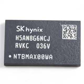
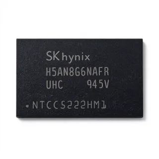
H5ANAG6NCR-PBC - 16Gb DDR4 SDRAM x16, FBGA-96 | SK hynix
部品番号: H5ANAG6NCR-PBC ✓ 生産中| 数量 | 単価 | 小計 |
|---|---|---|
| 1 | $85.23 | $85.23 |
| 10 | $81.5 | $815.00 |
| 100 | $77 | $7,700.00 |
| 500 | $73.5 | $36,750.00 |
| 1,000 | $70.2 | $70,200.00 |
H5ANAG6NCR-PBC 概要
DDR4 SDRAM is the fourth generation of Double Data Rate synchronous dynamic random-access memory, a class of volatile memory ICs that sits within the broader memory hierarchy of semiconductor devices. DDR4 doubles the internal bank count of its DDR3 predecessor, lowers the operating voltage from 1.5V to 1.2V, and adds bank-group architecture, giving designers higher bandwidth with lower power per transferred bit. A 16Gb monolithic die reduces component count per gigabyte versus stacked smaller dies.
Key features of this family include the 1.14V to 1.26V supply window that eases power-tree design, dynamic ODT for signal integrity on heavily loaded buses, and write leveling with ZQ calibration that simplifies high-speed PCB routing. The CRC function protects data integrity on the write path, while asynchronous reset enables deterministic power-up and error recovery.
Architecturally, the die uses bank-group parallelism so multiple banks can be interleaved within one burst window, sustaining high bus utilization. The x16 organization pairs well with 32-bit or 64-bit memory controllers using two or four devices, common in embedded and networking designs that do not need the module DIMM form factor.
Typical applications include embedded motherboards, industrial controllers, networking and telecom line cards, and consumer electronics boards built around DDR4 controllers from FPGA or processor vendors such as Intel (Altera) FPGA families.
Design considerations: adhere to the JEDEC DDR4 fly-by routing topology, length-match the data groups, and complete ZQ calibration during initialization; the exact speed grade designation and CAS latency for the PBC suffix are not stated in the retrieved data, so verify against the official SK hynix datasheet before finalizing controller timing.
This page synthesizes distributor availability data, same-package drop-in family alternatives, and practical design guidance beyond the raw manufacturer datasheet, giving engineers a faster path from selection to layout.
ドロップイン代替品: H5ANAG6NCR-PBC — 同一パッケージでピン互換。PCBの作り直しが必要な異なるパッケージの部品は除外されています。
このシリーズのバリエーション
同一シリーズでドロップイン互換のモデル: H5ANAG6NCR-PBC (同一形状・フットプリント) — 相違点: Package, Interface, Organization, Density, RoHS Status.
クイック比較ツール — 並列比較する代替部品を選択:
H5ANAG6NCJR-XNC
✅ ドロップイン✓ 在庫あり
$84.97 / 個
データシートを見る →H5ANAG6NBJR-PBC
✅ ドロップイン ⚠️ 仕様未検証✓ 在庫あり
$6.45 / 個
データシートを見る →H5ANAG6NBJR-UHC
✅ ドロップイン ⚠️ 仕様未検証✓ 在庫あり
$8.09 / 個
データシートを見る →H5ANAG6NAMR-UHC
✅ ドロップイン ⚠️ 仕様未検証✓ 在庫あり
$4.5 / 個
データシートを見る →H5ANAG6NBJR-RDC
✅ ドロップイン ⚠️ 仕様未検証✓ 在庫あり
$9.6 / 個
データシートを見る →H5ANAG6NCR-PBC 最大定格&電気的特性
| メモリタイプ | DDR4 SDRAM |
| Density | 16Gb (2GB) |
| メモリ構成 | x16 (1G x 16) |
| 電源電圧 | 1.14 V to 1.26 V (nominal 1.2 V) |
| パッケージ | FBGA-96 |
| Number of Terminals | 96 balls |
| 動作温度 | 0C to 85C |
| 実装タイプ | Surface Mount |
| Auto Self-Refresh | Yes |
| Auto Precharge | Yes |
| Asynchronous Reset | Yes |
| Data Mask | Yes |
| Dynamic ODT | Yes |
| ZQ Calibration | Yes |
| CRC Function | Yes |
| Write Leveling | Yes |
| RoHS ステータス | Compliant |
H5ANAG6NCR-PBC fbga-96 ピン配置ガイド
H5ANAG6NCR-PBC (fbga-96 パッケージ) のピン配置。 このデジタルICには、GPIO、通信インターフェース (UART、SPI、I2C)、および電源ピンが含まれています。代替ピン機能と設定オプションについては、メーカーのデータシートを参照してください。組み込みシステム設計とPCBレイアウトに不可欠です。

詳細なピン配置データはありません: H5ANAG6NCR-PBC.
詳細は データシート をご参照ください。
主な用途
H5ANAG6NCR-PBC の用途: 6 件s: Embedded Motherboard Main Memory, FPGA-Based Industrial Control Systems, Networking and Telecom Line Cards, Test and Measurement Instrumentation, Consumer Electronics Set-Top Boxes, Automotive-Adjacent ADAS Prototyping.
Embedded Motherboard Main Memory
The H5ANAG6NCR-PBC serves as main system memory on embedded x86 and ARM motherboards where SO-DIMM or UDIMM sockets are impractical. Each x16 device delivers 2GB on a 96-ball FBGA footprint, so four devices create an 8GB, 64-bit bank with minimal board area. The 1.14V to 1.26V supply window integrates cleanly with common 1.2V DC-DC rails, and dynamic ODT plus write leveling relax trace-length matching enough for 6-8 layer stackups. Place the devices on the controller fly-by bus and complete ZQ calibration during every boot; unlike DIMMs, soldered-down DRAM needs retraining after any die swap, so validate firmware training tables against the exact speed grade in your BOM.
おすすめ
FPGA-Based Industrial Control Systems
Industrial controllers built on Intel (Altera) Arria 10 or similar FPGA SoCs use the H5ANAG6NCR-PBC as buffer memory for motion control, machine vision, and real-time data logging. The 16Gb x16 organization matches the 64-bit DDR4 hard controller with four devices, and the family 3200 Mbps class supports heavy streaming bandwidth. The asynchronous reset pin allows the FPGA to deterministically reset the DRAM after watchdog events, improving recovery time in unattended factory equipment. Because industrial ambient temperatures stress timing margins, derate the controller frequency from the datasheet maximum, keep the 0C to 85C operating range in mind for uncooled cabinets, and mount decoupling capacitors on the back side directly beneath each FBGA-96 ball field.
おすすめ
Networking and Telecom Line Cards
Switch, router, and 5G baseband line cards consume large packet buffers, and four H5ANAG6NCR-PBC devices provide 8GB of deep buffering on a 64-bit bus. The DDR4 CRC function protects the write data path, an advantage in telecom systems where silent bit errors translate into corrupted payloads, and bank-group architecture sustains high bus utilization under random access patterns typical of packet queuing. The 96-ball FBGA package supports dense card layouts with devices on both sides of the board. Route the fly-by command/address bus with series termination at the controller end, respect per-byte length matching of roughly 25 mils skew, and budget the 1.2V rail at approximately 74 mA standby plus switching currents per device when sizing the power tree.
おすすめ
Test and Measurement Instrumentation
Oscilloscope, logic analyzer, and signal generator platforms capture gigabytes of sample data per acquisition, making the 16Gb-per-die H5ANAG6NCR-PBC an efficient capture memory. Four devices yield 8GB per 64-bit channel, and multiple channels scale in parallel. The family 3200 Mbps transfer class supports sustained write streaming from high-speed ADC front ends, while ZQ calibration maintains output impedance accuracy across the 0C to 85C range inside instruments with warm interiors. Because instrument downtime is costly, second-source flexibility matters: pin-compatible SK hynix family variants such as H5ANAG6NCJR-XNC can be swapped without PCB revision, requiring only a memory training table update in instrument firmware.
おすすめ
Consumer Electronics Set-Top Boxes
4K set-top boxes and smart-home gateways need 2-4GB of DDR4 for video decode buffers and application memory, and one or two H5ANAG6NCR-PBC devices meet this with a compact 96-ball FBGA footprint. The 1.2V nominal supply supports the low standby power budgets required for always-on voice-assistant designs, with family standby current around 74 mA maximum per the Vyrian terminal data. The x16 organization pairs naturally with cost-optimized SoCs that expose 16-bit or 32-bit DDR4 controllers. Consumer BOMs reward availability and price stability, so qualifying several speed-grade suffixes within the same H5ANAG6N family lets purchasing alternate between grades as commodity DRAM spot pricing moves.
おすすめ
Automotive-Adjacent ADAS Prototyping
ADAS prototype and dev-kit platforms gather camera, radar, and lidar streams into large frame buffers, and four H5ANAG6NCR-PBC devices supply 8GB per 64-bit controller channel at family-class bandwidth. Note that commodity DDR4 of this class is generally not AEC-Q100 qualified, so this part suits development platforms and non-safety production tiers rather than ASIL-rated modules; for automotive production, move to the vendor automotive-grade DRAM lines. During prototyping, the asynchronous reset input lets the SoC recover the DRAM after camera-pipeline faults without power cycling, and the CRC-enabled write path guards against frame corruption. Keep trace skews within JEDEC DDR4 guidance and re-run training whenever a die revision changes.
おすすめ
おすすめ製品の概要
エンジニアリング参考データ: H5ANAG6NCR-PBC — 比較、設計ガイダンス、コンプライアンス情報。
選定ガイド
代替品との比較
| パラメータ | この製品 | H5ANAG6NCJR-XNC | H5ANAG6NBJR-PBC | H5ANAG6NAMR-UHC |
|---|---|---|---|---|
| Package | FBGA-96 | FBGA-96 - same | FBGA-96 - same | FBGA-96 - same |
| Brand | SK Hynix | SK Hynix | SK Hynix | SK Hynix |
| Density | 16Gb (2GB) | 16Gb (2GB) | 16Gb (2GB) | 16Gb (2GB) |
| Organization | x16 | x16 | x16 | x16 |
| Supply Voltage | 1.14 V to 1.26 V | 1.14 V to 1.26 V | 1.14 V to 1.26 V | 1.14 V to 1.26 V |
| Dynamic ODT / ZQ Calibration / CRC | Yes / Yes / Yes | Yes / Yes / Yes | Yes / Yes / Yes | Yes / Yes / Yes |
| RoHS | Compliant | Compliant | Compliant | Compliant |
主な差別化要因
- 16Gb monolithic die minimizes component count (vs H5AN8G6NCJR-PBC)
- Full DDR4 feature set including CRC and dynamic ODT (vs H5ANAG6NAMR-UHC)
- Standard JEDEC DDR4 x16 footprint for second sourcing (vs H5ANAG6NCJR-XNC)
設計ノート
Route the DDR4 command/address bus in fly-by topology from the controller through each H5ANAG6NCR-PBC device, terminating at the last device. Length-match each x16 data byte group within the device ball field (target skew typically under 25 mils within a group). Dynamic ODT and write leveling relax the legacy DDR3 margin requirements, but do not skip per-byte length matching on 3200 Mbps-class buses; run IBIS simulation with the SK hynix IBIS model before tape-out.
Budget three rails: VDD and VDDQ at 1.2V nominal (1.14V-1.26V) plus VPP at 2.5V for the array pump. Distributor data indicates maximum standby current around 74 mA per device, but active read/write current on 16Gb dies can peak near 1 A per device transiently; size the VRM and bulk capacitance (at least 22 uF per device plus 0.1 uF per ball pair decoupling) accordingly. Estimated: a 4-device 64-bit bus at 1.2V can draw several amps active, so plan copper weight and rail sense points near the FBGA field.
Two frequent mistakes with this family: (1) confusing DDR4 with LPDDR4 - one distributor page mislabels the H5ANAG6N series as LPDDR4; it is standard DDR4 and is not interface-compatible with LPDDR4 controllers. (2) Ignoring the speed-grade suffix - PBC, XNC, and other suffixes carry different timing tables. Verify the PBC speed grade against the official SK hynix datasheet, configure controller CAS latency and tRCD from that table, and re-run memory training after any die-revision swap.
コンプライアンス情報
RoHS compliance stated by JLCPCB and LCSC listings for the H5ANAG6N family. Not AEC-Q100 qualified - commodity DDR4 for consumer/industrial use. REACH, halogen-free and conflict-minerals status not stated in retrieved data.