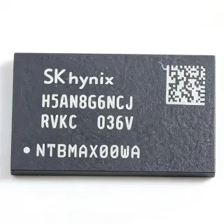
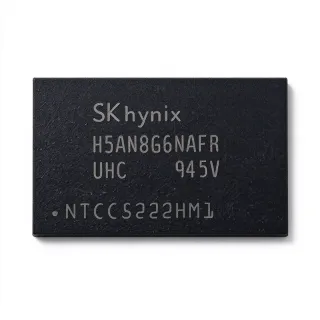
H5ANAG6NBJR-PBC - 16Gb DDR4 SDRAM DRAM Chip | SK hynix
MPN: H5ANAG6NBJR-PBC ✓ Active| Qty | Unit Price | Extended |
|---|---|---|
| 1 | $8.55 | $8.55 |
| 10 | $7.9 | $79.00 |
| 100 | $7.25 | $725.00 |
| 500 | $6.8 | $3,400.00 |
| 1,000 | $6.45 | $6,450.00 |
H5ANAG6NBJR-PBC Overview
DDR4 SDRAM is the mainstream generation of DRAM used as main system memory in PCs, servers, embedded controllers and networking equipment. Within the memory hierarchy it sits between caches/SSDs and storage, providing the large, fast working set that processors demand. The H5ANAG family belongs to SK hynix's 16Gb DDR4 portfolio, which the manufacturer positions as major DRAM for advanced compute, offering higher configurable densities than previous generations.
Key characteristics of this family include a 16Gb (2 GB) density per die, DDR4 architecture operating at a nominal 1.2 V supply - roughly 20% lower operating voltage than DDR3, reducing power per bit - and data rates up to the DDR4 generation maximum of 3200 MT/s across the portfolio. Verified family features include auto self-refresh, data mask (DM) function, asynchronous reset, dynamic on-chip termination (ODT), ZQ calibration, write leveling and CRC function.
Technically, the device is a CMOS DDR4 SDRAM implementing bank-group architecture with internal prefetch, supporting the JEDEC DDR4 feature set including bank groups, posted CAS and command/address training modes. The -PBC speed/temp code denotes a specific validated speed bin; verify the exact MT/s bin against the official SK hynix datasheet before final design sign-off.
Typical applications include main memory for desktop and notebook platforms, embedded computing modules, industrial controllers, networking line cards and set-top or consumer electronics that use x16 DDR4 memory down on the baseboard.
A key design consideration: DDR4 routing requires careful length matching of DQ/CA lines, correct VTT termination with dynamic ODT, and ZQ resistor placement; the 96-ball layout also constrains via fan-out, so plan layer stack-up early.
This page synthesizes verified web data, family feature sets, drop-in alternative candidates and practical design notes in one place - information not consolidated in the manufacturer datasheet.
Drop-in alternatives for H5ANAG6NBJR-PBC — same package, pin-to-pin compatible. Different-package parts requiring PCB rework are excluded.
Variants in this series
Same-series models that are drop-in compatible with H5ANAG6NBJR-PBC (same form factor and footprint) — differing in Package, Interface, Density, Data Rate, Asynchronous Reset.
Quick Comparison Tool — Select alternative parts for side-by-side comparison:
H5ANAG6NBJR-UHC
✅ Drop-In ⚠️ Specs Unverified✓ In Stock
$8.09 / Unit
View Datasheet →H5ANAG6NBJR-VKC
✅ Drop-In ⚠️ Specs Unverified✓ In Stock
$15 / Unit
View Datasheet →H5ANAG6NBJR-RDC
✅ Drop-In ⚠️ Specs Unverified✓ In Stock
$9.6 / Unit
View Datasheet →H5AN4G6NBJR-UHC
✅ Drop-In✓ In Stock
$8.09 / Unit
View Datasheet →H5AN4G6NBJR-PBC
✅ Drop-In✓ In Stock
$6.6 / Unit
View Datasheet →H5AN4G6NBJR-VKC
✅ Drop-In✓ In Stock
$12.96 / Unit
View Datasheet →H5ANAG6NBJR-PBC Maximum Ratings & Electrical Characteristics
| Memory Type | DDR4 SDRAM |
| Density | 16 Gb (2 GB) |
| Supply Voltage | 1.2 V |
| Generation Max Data Rate | 3200 MT/s (family max) |
| Package | FBGA-96 |
| Mounting Type | Surface Mount |
| Self Refresh | Auto self-refresh |
| Data Mask Function | Yes |
| Asynchronous Reset | Yes |
| On-Chip Termination | Dynamic ODT |
| ZQ Calibration | Yes |
| Write Leveling | Yes |
| CRC Function | Yes |
H5ANAG6NBJR-PBC fbga-96 Pin Configuration Guide
Pin configuration for H5ANAG6NBJR-PBC (fbga-96 package). This digital IC includes GPIO, communication interfaces (UART, SPI, I2C), and power pins. Refer to the manufacturer datasheet for alternate pin functions and configuration options. Essential for embedded system design and PCB layout.

No detailed pinout data available for H5ANAG6NBJR-PBC.
Refer to the datasheet for full pin configuration.
Typical Applications
H5ANAG6NBJR-PBC is suitable for 6 applications: Desktop and Notebook Main Memory, Embedded and Industrial Controllers, Networking and Communication Equipment, Consumer Electronics and Set-Top Boxes, Automotive and Rugged Telematics, Test, Measurement and Development Platforms.
Desktop and Notebook Main Memory
The H5ANAG6NBJR-PBC serves as main system memory in desktop, notebook and mini-PC platforms where 16Gb per chip allows large capacities from few components. Its 1.2 V DDR4 operation cuts memory power roughly 20% versus DDR3, per SK hynix, directly improving battery runtime and thermal headroom. Mounted on the baseboard or SODIMM, the x16 configuration in FBGA-96 halves the chip count needed for a given bus width compared with x8 parts. Dynamic ODT and write leveling simplify high-speed training at 2666-class data rates, while CRC supports link integrity on demand. For consumer platforms, the 16Gb density is the sweet spot between board area and total system RAM.
Recommended
Embedded and Industrial Controllers
Industrial controllers, HMI panels and edge-compute modules use the H5ANAG6NBJR-PBC as onboard main memory where extended temperature and long product lifecycles matter. The related NBJR family is documented to -40C to +95C operation with auto self-refresh (per LCSC data on H5AN4G6NBJR-UHC), supporting thermally harsh cabinets and fanless enclosures. Asynchronous reset allows deterministic memory state recovery after brown-out, and auto self-refresh preserves data through low-power idle states required by battery-backed and energy-harvesting nodes. Its FBGA-96 footprint suits two-layer-populated embedded boards where a single 16Gb chip replaces two 8Gb chips, saving board area and BOM positions.
Recommended
Networking and Communication Equipment
Switches, routers, 5G small cells and network line cards rely on large, fast working memory for packet buffering, flow tables and control-plane software. The H5ANAG6NBJR-PBC provides 2 GB per chip with DDR4-class bandwidth and CRC support that strengthens data integrity on the memory link - a feature explicitly listed for the NBJR family. The asynchronous reset pin allows the host CPU to re-initialize memory quickly after watchdog resets without full power cycling. With 3200 MT/s available across the SK hynix DDR4 portfolio, designers can size memory bandwidth to line-rate requirements while the 1.2 V rail eases PSU design in confined 1U chassis.
Recommended
Consumer Electronics and Set-Top Boxes
Set-top boxes, smart TVs, gaming accessories and IPTV gateways demand high memory density at aggressive cost points. The H5ANAG6NBJR-PBC delivers 16Gb (2 GB) in one FBGA-96 package, letting consumer SoCs with 32-bit or 64-bit x16 memory buses reach 4-8 GB with only two to four chips. Dynamic on-chip termination and ZQ calibration remove external termination components, trimming the BOM, while data-mask support simplifies partial writes used by video frame buffers. The 1.2 V supply aligns with mainstream SoC PMIC DDR4 rails, and the -PBC speed code matches the typical 2666 MT/s-class SoC integrations used in broadcast and streaming devices.
Recommended
Automotive and Rugged Telematics
Telematics control units, ADAS domain controllers and dashboard processors that use industrial-grade DDR4 in non-safety-critical memory partitions can integrate the H5ANAG6NBJR-PBC family. The NBJR series supports -40C to +95C operation with auto self-refresh, and dynamic ODT maintains signal integrity across wide temperature swings typical of engine-bay-adjacent modules. The asynchronous reset input supports ISO-style watchdog-driven recovery, and CRC adds a verification layer for memory links in vibration-prone environments. Automotive telematics boards benefit from 16Gb density per ball position, freeing PCB area under the module for LTE/GNSS transceivers. Validate the -PBC temperature code against your qualification plan before release.
Recommended
Test, Measurement and Development Platforms
Logic analyzers, protocol test equipment and FPGA-based DDR4 development boards use the H5ANAG6NBJR-PBC as a validated 16Gb training target. Its full DDR4 feature set - write leveling, ZQ calibration and dynamic ODT - makes it a comprehensive exercise for memory controller training algorithms on Xilinx and Intel FPGA platforms. A single chip provides 2 GB of scratch memory for waveform capture, enough for deep acquisition buffers without external SSD staging. Because the FBGA-96 footprint is shared across the 8Gb/16Gb NBJR family, test fixtures can swap H5AN4G6NBJR and H5ANAG6NBJR chips to characterize controller behavior across densities on identical hardware.
Recommended
Recommended Products Summary
Engineering reference data for H5ANAG6NBJR-PBC — comparison, design guidance, and compliance information.
Selection Guide
Comparison with Alternatives
| Parameter | This Product | H5ANAG6NBJR-UHC | H5AN4G6NBJR-UHC | H5AN4G6NBJR-VKC |
|---|---|---|---|---|
| Package | FBGA-96 | FBGA-96 - same | FBGA-96 - same | FBGA-96 - same |
| Brand | SK hynix | SK hynix | SK hynix | SK hynix |
| Density | 16 Gb (2 GB) | 16 Gb | 8 Gb | 8 Gb |
| Supply Voltage | 1.2 V | 1.2 V | 1.2 V | 1.2 V |
| Memory Type | DDR4 SDRAM | DDR4 SDRAM | DDR4 SDRAM | DDR4 SDRAM |
| Dynamic ODT | Yes | Yes | Yes | Yes |
| CRC Function | Yes | Yes | Yes | Yes |
| Asynchronous Reset | Yes | Yes | Yes | Yes |
Key Differentiators
- Double the density per footprint versus 8Gb siblings (vs H5AN4G6NBJR-PBC)
- Full DDR4 feature set for signal integrity training (vs H5AN4G6NBJR-UHC)
- 1.2 V operation versus older DDR3 (vs H5AN4G6NBJR-VKC)
Design Notes
Route DDR4 CA/clock lines in fly-by topology with VTT termination and enable dynamic ODT plus write leveling during controller training - the H5ANAG6NBJR-PBC supports both, per the verified family feature set. Keep DQ/DQS nets length-matched within each byte lane; for 2666 MT/s-class operation hold skew within controller spec (typically a few tens of mils intra-lane). Minimize via transitions on DQ nets and reference them to a continuous ground plane to control impedance discontinuities.
Provide a clean 1.2 V VDD/VDDQ rail per DDR4 specification (about 20% below the 1.5 V DDR3 rail, per SK hynix), a VTT termination rail at VDD/2 with bulk plus high-frequency decoupling, and the VPP auxiliary rail per the official datasheet. Budget current using the datasheet IDD tables for the -PBC speed bin at your operating frequency and temperature. Place bulk capacitance near the FBGA balls and 0.1 uF ceramics at each supply ball group; validate with a power integrity simulation before tape-out.
Place the ZQ calibration resistor close to the ZQ ball with a short, direct trace to ground through the datasheet-specified precision resistor (typically 240 ohm 1% for DDR4 - confirm in the official SK hynix datasheet). Do not route other signals near ZQ. Plan the FBGA-96 fan-out in the layer stack-up early: dog-leg via escape or inner-layer escape for center balls. Confirm the exact -PBC temperature range and speed bin from the official datasheet before qualification; web listings do not state these for this exact code.
Compliance Information
Compliance status not stated in the provided web data; confirm on the official SK hynix product page or datasheet.