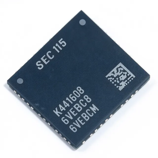
K4RAH086VE-BCWM - DDR5 16Gb 5600Mbps DRAM | Samsung Electronics
部品番号: K4RAH086VE-BCWM ✓ 生産中| 数量 | 単価 | 小計 |
|---|---|---|
| 1 | $9.8 | $9.80 |
| 10 | $9.2 | $92.00 |
| 100 | $8.6 | $860.00 |
| 500 | $8.1 | $4,050.00 |
| 1,000 | $7.6 | $7,600.00 |
K4RAH086VE-BCWM 概要
DRAM (Dynamic Random Access Memory) is the primary working memory of modern computing systems; DDR5 SDRAM is the fifth generation of the double-data-rate synchronous DRAM family, succeeding DDR4 in the memory hierarchy of PCs, servers, and gaming platforms. DDR5 doubles bank groups and doubles prefetch (16n vs 8n), integrates an on-die power management IC, and delivers higher effective bandwidth at lower per-bit power than DDR4.
Key features of the K4RAH086VE-BCWM include its 16 Gb density per chip in a x8 organization (2G x 8), a 5600 Mbps pin speed supporting DDR5-5600 modules (PC5-44800 class), and the low 1.1V core supply of the JEDEC DDR5 standard that reduces dynamic power versus the 1.2V of DDR4.
The device uses Samsung advanced DRAM process technology in an 82-ball fine-pitch ball grid array (FBGA) surface-mount package, the standard footprint for discrete DDR5 components used on UDIMMs, RDIMMs, SODIMMs, and soldered-down memory for embedded and client computing boards.
Typical applications include desktop and notebook PC main memory modules, gaming memory, workstations, and computing systems that require high-bandwidth main memory. As a DDR5 component it pairs with DDR5 memory controllers in CPUs and with module-level PMICs and registering clock drivers on RDIMM designs.
Design consideration: DDR5 signal integrity at 5600 Mbps demands careful length-matched fly-by routing, on-die termination configuration, and reference voltage (VDDQ) decoupling per JEDEC DDR5 module design guidance.
This page synthesizes distributor sourcing data, drop-in alternatives, and practical design notes not found in the manufacturer datasheet.
ドロップイン代替品: K4RAH086VE-BCWM — 同一パッケージでピン互換。PCBの作り直しが必要な異なるパッケージの部品は除外されています。
このシリーズのバリエーション
同一シリーズでドロップイン互換のモデル: K4RAH086VE-BCWM (同一形状・フットプリント) — 相違点: Interface, Package, Data Rate, Density, Organization.
クイック比較ツール — 並列比較する代替部品を選択:
K4RAH086VB-BCWM
✓ 在庫あり
$44.5455 / 個
データシートを見る →K4RAH086VP-BCWM
✓ 在庫あり
価格はお問い合わせください
データシートを見る →K4RAH086VB-BIWM
✓ 在庫あり
$4.85 / 個
データシートを見る →K4RAH086VB-BCQK
✓ 在庫あり
$41.0156 / 個
データシートを見る →K4RAH165VB-BCWM
✓ 在庫あり
$9.92 / 個
データシートを見る →K4RAH086VE-BCWM 最大定格&電気的特性
| メモリタイプ | DDR5 SDRAM |
| Density | 16 Gb |
| メモリ構成 | 2G x 8 |
| データレート | 5600 Mbps |
| Supply Voltage (VDD) | 1.1 V |
| パッケージ | 82-ball FBGA |
| 実装タイプ | Surface Mount |
| 動作温度 | 0C to +85C |
| Generation | DDR5 |
| ライフサイクル状態 | Mass Production |
| Manufacturer | Samsung Electronics |
K4RAH086VE-BCWM 82-ball fbga ピン配置ガイド
K4RAH086VE-BCWM (82-ball fbga パッケージ) のピン配置。 このデジタルICには、GPIO、通信インターフェース (UART、SPI、I2C)、および電源ピンが含まれています。代替ピン機能と設定オプションについては、メーカーのデータシートを参照してください。組み込みシステム設計とPCBレイアウトに不可欠です。

詳細なピン配置データはありません: K4RAH086VE-BCWM.
詳細は データシート をご参照ください。
主な用途
K4RAH086VE-BCWM の用途: 6 件s: Desktop PC Main Memory (UDIMM), Gaming Memory Modules, Notebook and SODIMM Memory, Client Computing Motherboards (Soldered-Down Memory), Industrial Computing and Edge Systems, Workstation and Entry Server Memory (RDIMM).
Desktop PC Main Memory (UDIMM)
The K4RAH086VE-BCWM's 16Gb density and DDR5-5600 speed make it a core building block for desktop DDR5 UDIMMs. Eight x8 chips populate a 16GB single-rank module; sixteen chips create a 32GB dual-rank configuration. At 5600 Mbps per pin, a 64-bit module achieves roughly 44.8 GB/s of peak bandwidth (PC5-44800 class), matching current mainstream desktop platform memory specifications. The 1.1V VDD of the JEDEC DDR5 standard, combined with the module-level 5V-to-1.1V PMIC, keeps module power below comparable DDR4 designs while delivering higher bandwidth. Designers must follow JEDEC UDIMM layout rules for fly-by CA routing and per-byte DQ length matching to the FBGA balls.
おすすめ
Gaming Memory Modules
Samsung positions the K4RAH086 family specifically for PC and gaming applications. The 5600 Mbps speed bin supports enthusiast DDR5-5600 kits, and the 2G x 8 organization is favored for overclocking-oriented module designs because of its 16-bank-group architecture and on-die termination granularity. Low 1.1V operation gives headroom for VDD/Q overclocking within PMIC limits. Gaming module makers pair these DRAMs with programmable register-less SPD hubs (SPD5118-class) to expose XMP 3.0 profiles. Signal integrity at 5600 Mbps on four-layer consumer module PCBs requires the short trace lengths typical of UDIMM form factors, which the 82-ball FBGA footprint supports with dense ball-out routing.
おすすめ
Notebook and SODIMM Memory
In notebook designs, the K4RAH086VE-BCWM's x8 organization and 16Gb density allow compact SODIMM configurations: eight chips yield a 16GB module within the 260-pin DDR5 SODIMM form factor. The 1.1V supply directly reduces platform power draw, extending battery life relative to 1.2V DDR4 solutions of equal capacity. DDR5's on-die power management and lower VDDQ reduce module thermal load, important in thermally constrained chassis. The 82-ball FBGA package is compatible with the low-profile component height limits of SODIMM assembly, and the 0C to +85C commercial range covers typical laptop ambient specifications. Designers should verify chipset DDR5-5600 support and memory-down training firmware compatibility.
おすすめ
Client Computing Motherboards (Soldered-Down Memory)
For motherboards with memory-down (soldered) DRAM, the K4RAH086VE-BCWM can be placed directly on the PCB, saving the SODIMM connector cost and height. Its 82-ball FBGA reflows onto standard OSP-finish PCB pads, and four chips provide 8GB, eight chips 16GB of soldered memory per platform. DDR5 memory-down designs must implement the same 1.1V PMIC power tree and CA/DQS training flow as modules, but gain improved signal integrity from short, controlled-impedance traces. The 0C to +85C range suits client and commercial desktop ambient requirements. This approach is common in mini-PCs, Chromebooks, and cost-optimized desktop boards where socketed upgradeability is not required.
おすすめ
Industrial Computing and Edge Systems
While the VE-BCWM suffix is the commercial temperature grade, the same-die industrial variant K4RAH086VB-BIWM extends the family into industrial PCs, edge servers, and networking appliances operating from -40C. DDR5-5600 bandwidth supports modern edge AI inference accelerators and multi-core industrial processors that saturate DDR4 bandwidth. On-die ECC in DDR5 improves data reliability for long-life unattended deployments, complementing link-level RCD parity on registered designs. System designers using this part in industrial platforms should specify the BI suffix for extended temperature, or qualify the BC grade only for 0C to +85C ambient environments per Samsung datasheet derating guidance.
おすすめ
Workstation and Entry Server Memory (RDIMM)
The 16Gb density of the K4RAH086VE-BCWM enables high-capacity workstation and entry-server RDIMMs: a dual-rank 32GB RDIMM uses sixteen x8 chips, and 64GB configurations are possible with 32Gb die or higher chip counts. In RDIMM designs, the DRAM connects through a registering clock driver (RCD) and the module PMIC manages the 1.1V and 1.8V VPP rails. DDR5's on-die ECC plus side-band CRC improves RAS features required in workstation-class platforms. The 5600 Mbps bin aligns with current workstation CPU memory controllers. Verify CPU memory-qualified vendor list (QVL) inclusion of the exact die revision before production RDIMM builds.
おすすめ
おすすめ製品の概要
エンジニアリング参考データ: K4RAH086VE-BCWM — 比較、設計ガイダンス、コンプライアンス情報。
選定ガイド
代替品との比較
| パラメータ | この製品 | K4RAH086VB-BCWM | K4RAH086VP-BCWM | K4RAH086VB-BIWM | K4RAH165VB-BCWM |
|---|---|---|---|---|---|
| Package | 82-ball FBGA | 82-ball FBGA - same | 82-ball FBGA - same | 82-ball FBGA - same | 82-ball FBGA - same (x4 ball-out) |
| Brand | Samsung Electronics | Samsung Electronics | Samsung Electronics | Samsung Electronics | Samsung Electronics |
| Density | 16 Gb | 16 Gb | 16 Gb | 16 Gb | 16 Gb |
| Organization | 2G x 8 | 2G x 8 | 2G x 8 | 2G x 8 | 4G x 4 |
| Data Rate | 5600 Mbps | 5600 Mbps | 5600 Mbps | 5600 Mbps | 5600 Mbps |
| Supply Voltage | 1.1 V | 1.1 V | 1.1 V (VPP variant) | 1.1 V | 1.1 V |
| Operating Temperature | 0C to +85C | 0C to +85C | 0C to +85C | -40C to +85C (industrial) | 0C to +85C |
| Die Revision / Suffix | VE (B-die generation) | VB die revision | VP variant | VB die, industrial temp | VB die, x4 organization |
主な差別化要因
- DDR5-5600 speed bin for mainstream platforms (vs K4A8G085WB)
- Industrial temperature option in same footprint (vs K4RAH086VB-BIWM)
- x8 organization for mainstream module architectures (vs K4RAH165VB-BCWM)
設計ノート
At 5600 Mbps, DDR5 DQ and DQS traces must be impedance-controlled (typically 40 ohm for DQ on modules) and length-matched within tight per-byte skew budgets. Follow the Samsung DDR5 datasheet layout guideline: fly-by routing for CA signals, per-byte length matching for DQ/DQS/DM, and reference-plane-continuous routing under all memory nets. Simulation with the IBIS models from Samsung is strongly recommended before first silicon.
The K4RAH086VE-BCWM runs from a 1.1V VDD with a separate VDDQ rail per DDR5 JEDEC definition. Provide dense decoupling (multiple 0.1uF plus bulk 10uF+ ceramics) immediately beneath the 82-ball FBGA via fanout, and use the DDR5 module PMIC (5V input) per JEDEC DDR5 specification for UDIMM/RDIMM designs. Estimated: a single-rank 16GB module at full bandwidth can draw several watts; size the PMIC and copper accordingly.
Do not interchange die revisions (VE vs VB) without checking the CPU memory controller qualified vendor list (QVL) - training algorithms and DFE settings can differ between revisions. Also confirm the x8 vs x4 organization matches your module design: K4RAH165 (x4) parts have different DQ ball assignments than K4RAH086 (x8) parts and are not drop-in interchangeable at the system level.
コンプライアンス情報
Compliance data not present in provided web data; consult the official Samsung Semiconductor environmental documentation for K4RAH086VE-BCWM.



