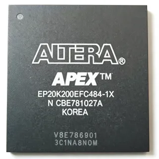
EP1S10F484C6N - Stratix FPGA, 10,570 LEs, 484-FBGA | Intel
MPN: EP1S10F484C6N ✗ End of Life| Qty | Unit Price | Extended |
|---|---|---|
| 1 | $353.61 | $353.61 |
| 10 | $318.25 | $3,182.50 |
| 100 | $282.89 | $28,289.00 |
| 250 | $254.6 | $63,650.00 |
| 500 | $226.31 | $113,155.00 |
EP1S10F484C6N Overview
An FPGA (Field Programmable Gate Array) is a semiconductor device containing an array of configurable logic blocks (CLBs/LABs), programmable interconnects, and I/O cells that the designer can program after manufacture to implement arbitrary digital logic. FPGAs occupy a position in the system hierarchy between fixed-function ASICs and software-driven microcontrollers: they offer ASIC-class performance and parallelism while preserving the flexibility of software-based design. Stratix FPGAs in particular were Intel (formerly Altera)'s high-performance, DSP-rich family targeting communications infrastructure, video processing, and military/aerospace applications.
Key features of the EP1S10F484C6N include: 1,057 LABs/CLBs (10,570 logic cells), 920 Kbits of embedded RAM, built-in PLLs for clock management, support for multiple I/O standards (LVTTL, LVCMOS, PCI, SSTL, HSTL, LVDS), dedicated multiplier/DSP blocks for high-throughput arithmetic, and configuration via JTAG or passive/active serial/parallel modes. The Stratix architecture introduced the TriMatrix memory structure with three block sizes (M512, M4K, M-RAM) optimized for different datapath widths.
Architecturally, the device combines row-based LABs, column-based embedded memory and DSP blocks, and surrounding I/O rings, all interconnected by a multi-level routing hierarchy. The 130 nm process allows core voltages down to 1.5 V with low static power; supply range is 1.425 V to 1.575 V. Configuration data is stored in SRAM cells and must be loaded at each power-up from a configuration PROM or a processor.
Typical applications include telecommunications infrastructure (SONET/SDH framer, protocol bridges), DSP co-processing for medical imaging and military radar, high-speed serial protocol bridging, video broadcast equipment, and ASIC prototyping. The combination of DSP blocks, ample block RAM, and high I/O count makes the EP1S10F484C6N a strong fit for parallel datapath and pipelined DSP workloads.
When designing with this device, ensure the Quartus II design software version supports the Stratix I family (Quartus II 13.0 or earlier is required for legacy support). The FBGA-484 package requires careful PCB layout with microvia or via-in-pad technology to fan out the 1.0 mm pitch ball array; thermal management relies on the exposed die-side thermal pad and adequate board copper.
This page consolidates distributor pricing, drop-in alternatives within the Stratix I family, and practical design notes that supplement the manufacturer datasheet with sourcing and lifecycle context.
Drop-in alternatives for EP1S10F484C6N — same package, pin-to-pin compatible. Different-package parts requiring PCB rework are excluded.
Variants in this series
Same-series models that are drop-in compatible with EP1S10F484C6N (same form factor and footprint) — differing in Package, Family, Operating Temperature, Mounting Type, Configuration Method.
Quick Comparison Tool — Select alternative parts for side-by-side comparison:
EP1S10F484C7N
✅ Drop-In✓ In Stock
$162 / Unit
View Datasheet →EP1S10F484C5N
✅ Drop-In✓ In Stock
$52 / Unit
View Datasheet →EP1S10F484I6N
✅ Drop-In✓ In Stock
$305.2 / Unit
View Datasheet →EP1S10F484C6N Maximum Ratings & Electrical Characteristics
| Family | Stratix |
| Logic Elements / Cells | 10,570 |
| Number of LABs / CLBs | 1,057 |
| Total RAM Bits | 920,448 |
| Number of User I/O | 335 |
| Package | 484-FBGA (23 × 23 mm, 1.0 mm pitch) |
| Process Technology | 130 nm CMOS |
| Supply Voltage - Operating | 1.425 V to 1.575 V (core 1.5 V) |
| Speed Grade | C6 |
| Operating Temperature | 0 °C to 85 °C (TJ) |
| Mounting Type | Surface Mount (SMT) |
| Lead Free | Yes |
| Configuration Method | SRAM - volatile (JTAG / passive serial / passive parallel / fast passive parallel) |
| I/O Standards Supported | LVTTL, LVCMOS, PCI, SSTL, HSTL, LVDS |
| On-chip Resources | TriMatrix memory (M512, M4K, M-RAM), DSP blocks, PLLs |
EP1S10F484C6N 484-fbga (23 × 23 mm, 1.0 mm pitch) Pin Configuration Guide
Pin configuration for EP1S10F484C6N (484-fbga (23 × 23 mm, 1.0 mm pitch) package). This digital IC includes GPIO, communication interfaces (UART, SPI, I2C), and power pins. Refer to the manufacturer datasheet for alternate pin functions and configuration options. Essential for embedded system design and PCB layout.

No detailed pinout data available for EP1S10F484C6N.
Refer to the datasheet for full pin configuration.
Typical Applications
EP1S10F484C6N is suitable for 6 applications: Telecommunications Infrastructure (SONET/SDH Framer, Protocol Bridge), DSP Co-Processing for Medical Imaging / Military Radar, Video Broadcast Equipment and Image Processing, ASIC Prototyping and Emulation, Industrial Control and High-Speed Datapath Controllers, Legacy Avionics and Military Communications.
Telecommunications Infrastructure (SONET/SDH Framer, Protocol Bridge)
The EP1S10F484C6N's 10,570 logic elements, 920 Kbit TriMatrix embedded RAM, and 335 user I/O pins make it well-suited for telecommunications line-card designs such as SONET/SDH framers, OTN mappers, and protocol bridges. The high I/O count supports parallel connection to multiple PHYs and SERDES companion chips, while the DSP blocks perform clock-and-data-recovery assist and framer overhead processing. The C6 speed grade at ~390 MHz internal Fmax is sufficient for OC-48/STM-16 datapath widths. Engineers commonly pair the EP1S10F484C6N with external PHY devices and a configuration PROM for non-volatile SRAM load at boot. Note that newer Stratix families (II/III/IV) offer integrated transceivers, which the Stratix I lacks.
Recommended
DSP Co-Processing for Medical Imaging / Military Radar
The EP1S10F484C6N integrates dedicated multiplier/DSP blocks alongside 10,570 logic elements, making it a strong fit for DSP co-processing in medical imaging (ultrasound beamforming, MRI reconstruction pre-processing) and military radar pulse-Doppler pipelines. The TriMatrix block RAM (M512, M4K, M-RAM) provides the data FIFOs required for streaming ADC samples at rates up to hundreds of MSPS, while the LAB fabric implements FIR filters, FFT butterflies, and window functions. The 335 available I/Os fan out to multi-channel ADC front ends and synchronization buses. Compared to a software DSP, the FPGA delivers deterministic latency and 10-100x throughput per watt on parallel kernels. Verify thermal management under sustained DSP load; the FBGA-484 package requires board-level copper for heat spreading.
Recommended
Video Broadcast Equipment and Image Processing
The EP1S10F484C6N serves video broadcast workflows including SD/HD-SDI cross-points, format converters, and real-time image-processing overlays. Its 335 user I/Os accommodate multiple SDI inputs and outputs (each requiring several LVDS pairs for clock and data), while the 10,570 LEs implement color-space conversion, scaling, de-interlacing, and on-screen display mixers. The TriMatrix block RAM stores video line buffers and frame buffers for temporal processing; the DSP blocks accelerate motion-adaptive algorithms. The C6 speed grade meets 148.5 MHz pixel clocks needed for 720p/1080i HD-SDI. Engineers often use the EP1S10F484C6N alongside an external SDI equalizer and a video A/D or D/A converter. For modern 4K workflows, designers have migrated to Stratix IV/V or current families with integrated transceivers.
Recommended
ASIC Prototyping and Emulation
With 10,570 logic elements and 335 user I/Os, the EP1S10F484C6N is used as a building block in multi-FPGA ASIC prototyping platforms where several FPGAs are stacked or arrayed to emulate larger ASIC designs. The Stratix I architecture is well-documented in Quartus II synthesis, supporting rapid RTL bring-up of ASIC-equivalent logic and memory subsystems. The device's abundant block RAM serves as scratchpad memory for transaction-level modeling. The FBGA-484 package is compatible with standard prototyping daughter-cards and socket carriers. Compared with newer families, Stratix I has lower leakage and predictable timing closure, which simplifies prototype-to-ASIC correlation. Engineers targeting >5M gates typically use multiple Stratix I or upgrade to Stratix II/III for higher density per device.
Recommended
Industrial Control and High-Speed Datapath Controllers
The EP1S10F484C6N is applied in industrial control systems where deterministic hardware logic drives motors, sensors, and high-speed data acquisition. Its 335 user I/Os support parallel connection to multi-axis motion controllers, encoder feedback, and isolated digital I/O racks; the embedded DSP blocks implement field-oriented control (FOC) loops and FFT-based vibration analysis. The commercial 0-85 °C temperature range suits factory-floor enclosures; the industrial-grade EP1S10F484I6N is preferred for uncontrolled-temperature deployments. Compared with microcontroller-only solutions, the FPGA delivers deterministic sub-microsecond response times and parallel processing of multiple control loops. Designers commonly pair the EP1S10F484C6N with isolated gate drivers, encoder interfaces, and Ethernet PHYs for control networking.
Recommended
Legacy Avionics and Military Communications
The EP1S10F484C6N appears in long-lifecycle avionics and military communication systems that were designed in the early 2000s and continue in service today. Its combination of 10,570 logic elements, 335 I/Os, and SRAM-based reconfigurability suits MIL-STD-1553 and ARINC 429 bus interfaces, as well as secure voice and data processing subsystems. The commercial 0-85 °C temperature range is acceptable for temperature-controlled avionics bays; ruggedized variants use the EP1S10F484I6N industrial-grade equivalent. Because these platforms have multi-decade service lives, lifecycle risk on the EP1S10F484C6N is actively managed via approved broker sources and pre-positioned safety stock. Migration to newer families is constrained by re-qualification cost and unchanged form factor requirements.
Recommended
Recommended Products Summary
Engineering reference data for EP1S10F484C6N — comparison, design guidance, and compliance information.
Selection Guide
Comparison with Alternatives
| Parameter | This Product | EP1S10F484C7N | EP1S10F484C5N | EP1S10F484I6N |
|---|---|---|---|---|
| Brand | Intel (formerly Altera) | Intel | Intel | Intel |
| Package | FBGA-484 (23x23, 1.0 mm pitch) | FBGA-484 (same) | FBGA-484 (same) | FBGA-484 (same) |
| Logic Elements | 10,570 | 10,570 | 10,570 | 10,570 |
| LABs / CLBs | 1,057 | 1,057 | 1,057 | 1,057 |
| Total RAM Bits | 920,448 | 920,448 | 920,448 | 920,448 |
| User I/O | 335 | 335 | 335 | 335 |
| Speed Grade | C6 (~390 MHz core) | C7 (faster) | C5 (slower) | C6 (same) |
| Operating Temperature | 0 to 85 °C (commercial) | 0 to 85 °C (commercial) | 0 to 85 °C (commercial) | -40 to 100 °C (industrial) |
| Supply Voltage | 1.5 V (1.425 to 1.575 V) | 1.5 V | 1.5 V | 1.5 V |
| Lifecycle Status | Obsolete | Obsolete | Obsolete | Obsolete |
Key Differentiators
- Stratix I family - established FPGA architecture with mature Quartus II tool support (vs Newer Stratix IV/V devices)
- 130 nm CMOS process - lower leakage than scaled-node FPGAs at idle (vs Stratix IV (40 nm))
- 335 user I/Os - abundant parallel I/O for multi-channel DSP and protocol fan-out (vs Cyclone III EP3C40 (535 LE, 535 I/O is less LE))
Design Notes
The EP1S10F484C6N requires multiple supply rails: VCCINT (1.5 V core), VCCIO (per bank, 1.5/1.8/2.5/3.3 V), VCCPD (3.3 V pre-driver), and VCCAUX (2.5 V PLLs and auxiliary). Each rail must be brought up in the sequence specified by the Stratix I pin connection guidelines; failure to sequence can cause latch-up. A power supervisor with adjustable sequencing (e.g., TPS3808 or similar) is recommended. Add 100 µF of bulk capacitance plus 0.1 µF + 10 µF decoupling per bank as a starting point. Estimated: with all rails loaded, a fully utilized EP1S10F484C6N draws ~0.5-1.5 A on VCCINT at C6 grade.
The FBGA-484 package (23 × 23 mm, 1.0 mm pitch) has theta-JA around 18-22 °C/W on a standard JEDEC test board with adequate thermal vias under the die. Under heavy DSP utilization, junction temperature can rise 20-40 °C above ambient; commercial-grade limits require junction below 85 °C. Add a thermal pad footprint with an array of 0.3 mm thermal vias to an internal copper plane. For enclosed industrial environments, derate by 10-15 °C. Estimated: at 1.5 W dissipation, junction rise is roughly 30 °C above ambient on a 4-layer board with thermal vias.
Route the FBGA-484 escape on inner layers using microvia-in-pad or 0.15 mm via technology; a 1.0 mm pitch BGA cannot be reliably escaped on two layers with conventional through-vias. Maintain 50 Ω impedance on all high-speed signals (LVDS, DDR, clock). Place the configuration PROM within 6 inches of the FPGA to meet the passive serial timing budget. Use a 4-layer stack-up with continuous ground planes adjacent to signal layers for return path integrity. Per Quartus II board design guidelines, avoid stubs on clock traces and series-terminate clocks at the source.
Do not leave MSEL pins floating - they select the configuration mode (AS, PS, FPP, JTAG) and incorrect setting prevents the FPGA from configuring. Ensure nCONFIG is pulled high through a 10 kΩ resistor and nSTATUS is monitored by the system controller. The TriMatrix RAM blocks support mixed-width read/write; if your design depends on a specific width, verify the Quartus II inferred-RAM report. Do not exceed the absolute maximum VCCINT of 1.65 V during hot-plug events - add a hot-swap controller or inrush limiter if the FPGA is on a plug-in card.
Compliance Information
Lead-free FBGA-484 package per 'N' suffix in MPN. RoHS compliance confirmed by Intel Altera product documentation. Not AEC-Q100 qualified - this is a commercial-grade FPGA. Halogen-free status not explicitly stated in provided data.