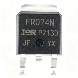
FDD8880 - 30V 58A N-Ch PowerTrench MOSFET | onsemi
MPN: FDD8880 ⚠ Last Time Buy| Qty | Unit Price | Extended |
|---|---|---|
| 1 | $1.2 | $1.20 |
| 10 | $1.08 | $10.80 |
| 100 | $0.92 | $92.00 |
| 500 | $0.8 | $400.00 |
| 1,000 | $0.68 | $680.00 |
FDD8880 Overview
A power MOSFET is a voltage-controlled semiconductor switch used to regulate or switch electrical power in circuits. Within the power-management hierarchy, discrete MOSFETs sit alongside integrated drivers and controllers, and the DPAK (TO-252AA) package family is one of the most widely used surface-mount power packages, providing a large exposed tab that solders directly to the PCB copper for heat spreading.
The FDD8880 was specifically designed to improve the overall efficiency of DC/DC converters using synchronous or conventional switching PWM controllers. Its key differentiators are low gate charge, low rDS(on), and fast switching speed - three parameters that together minimize conduction and switching losses in high-frequency power conversion.
Architecturally, the PowerTrench process uses a low charge, low resistance trench structure that reduces gate charge without sacrificing on-resistance. This makes the device well suited to high-frequency synchronous rectification, where total gate charge directly drives driver losses and switching speed affects transition losses.
Typical applications include synchronous buck converters in point-of-load power supplies, DC/DC converter modules, and high-current load switches where a 30 V breakdown rating provides margin for 12 V rails and transient events.
Design consideration: with 9 mOhm on-resistance, conduction losses at high current are significant (Estimated: I^2 x R gives ~0.34 W at 6.2 A, rising quadratically), so thermal design of the PCB copper area under the tab is critical.
This page synthesizes distributor data, lifecycle status, drop-in alternatives, and practical design notes not consolidated in the manufacturer datasheet.
Drop-in alternatives for FDD8880 — same package, pin-to-pin compatible. Different-package parts requiring PCB rework are excluded.
Variants in this series
Same-series models that are drop-in compatible with FDD8880 (same form factor and footprint) — differing in Package, Technology.
Quick Comparison Tool — Select alternative parts for side-by-side comparison:
FDD8880-G
✅ Drop-In📋 Reference alternative (not in catalog)
FDD8896
✅ Drop-In✓ In Stock
$0.62 / Unit
View Datasheet →FDD8880-VB
✅ Drop-In📋 Reference alternative (not in catalog)
FDD8880 Maximum Ratings & Electrical Characteristics
| Polarity | N-Channel |
| Drain-Source Voltage (VDS) | 30 V |
| Continuous Drain Current (ID) | 13 A (Ta), 58 A (Tc) |
| On-Resistance (rDS(on)) | 9 mOhm max |
| Total Power Dissipation (PD) | 55 W (Tc) |
| Technology | PowerTrench |
| Package | TO-252AA (DPAK) |
| Mounting Type | Surface Mount |
| Configuration | Single FET |
| Lifecycle Status | Last Shipments |
FDD8880 Pin Configuration
| Pin 1 | Gate — Gate terminal - drive with PWM gate signal through a series resistor |
| Pin 2 | Drain (Tab) — Drain connection via exposed tab; solder to copper pour for heat dissipation |
| Pin 3 | Source — Source terminal - power return path |
Safe Operating Area
Typical Applications
FDD8880 is suitable for 6 applications: Synchronous Buck Converters, DC/DC Converter Modules, High-Current Load Switches, Point-of-Load Power Supplies, Motor Drive Half-Bridges, Battery-Powered Inverters and UPS.
Synchronous Buck Converters
The FDD8880 was purpose-built for synchronous DC/DC converters, and it excels as the low-side (sync) FET in buck converters for 12 V rails. Its 9 mOhm maximum on-resistance minimizes I^2R conduction loss during the freewheeling interval, while low gate charge reduces driver loss and speeds up the switching transition, directly improving converter efficiency at high frequency. Placed after a PWM controller with an appropriate gate driver, the 30 V VDS rating provides comfortable margin above 12 V bus transients. Estimated: at 15 A output, conduction loss is roughly 2 W during the freewheeling duty interval, so PCB copper under the tab must be sized for it.
Recommended
DC/DC Converter Modules
Brick-style and onboard DC/DC converter modules benefit from the FDD8880's balance of low rDS(on) and low total gate charge, which per the onsemi datasheet were the two optimization targets of the PowerTrench design. In a module using either synchronous or conventional PWM control, the FDD8880 can serve as the primary switching element for 30 V-class inputs, and its 58 A (Tc) rating supports high-current paralleled-FET topologies. Because the part is DPAK-packaged, module vendors gain a compact surface-mount power stage with the exposed tab soldered to an internal copper bus for heat removal, keeping the module footprint small while delivering tens of amps.
Recommended
High-Current Load Switches
With 58 A continuous capability at case temperature and only 9 mOhm of on-resistance, the FDD8880 works as a primary-side load switch for 12 V and 24 V-class distribution rails where a 30 V rating provides transient headroom. When driven fully on with 10 V gate drive, the device behaves almost as a closed switch - Estimated: at 10 A the drop is only ~90 mV and dissipation ~0.9 W, negligible for most racks and backplanes. A series gate resistor and a pull-down to hold the FDD8880 off during power-up sequencing prevent transient shoot-through. Designers should verify inrush energy against the datasheet safe operating area during hot-plug events.
Recommended
Point-of-Load Power Supplies
Point-of-load (POL) regulators converting a 12 V intermediate bus down to sub-1 V core voltages rely on the sync FET for the majority of conduction loss, making the FDD8880's 9 mOhm rDS(on) a direct efficiency contributor. Its low gate charge also keeps the controller's gate-drive budget small at the 300 kHz to 1 MHz switching frequencies typical of POL designs. In this topology the FDD8880 operates at low duty cycle on the low side, so its fast switching speed minimizes body-diode conduction time before turn-on. Because the part is now in Last Shipments status, POL designers starting new boards should validate the FDD8880-G variant to secure long-term supply.
Recommended
Motor Drive Half-Bridges
Low-voltage DC motor drives (12 V/24 V automotive and industrial fans, pumps, actuators) can use pairs of FDD8880 devices in a half-bridge configuration with a high/low-side gate driver. The 30 V rating covers inductive kick from motor windings when clamped by free-wheeling action, while 9 mOhm on-resistance keeps stall-current conduction losses manageable - Estimated: a 20 A stall current dissipates about 3.6 W per device, acceptable with proper copper area. Low gate charge permits PWM frequencies in the 20 kHz range with low driver loss and quiet acoustic operation. Body-diode conduction during dead-time adds loss, so dead-time should be minimized within safety limits.
Recommended
Battery-Powered Inverters and UPS
Low-voltage battery inverters and DC UPS systems switching 12 V or 24 V battery stacks need 30 V-class N-channel power FETs with minimal conduction loss, and the FDD8880's 9 mOhm, 58 A (Tc) rating fits push-pull or half-bridge stages of these converters. Low gate charge reduces the standby drive loss that erodes efficiency at light load - important in always-on UPS front ends. In such systems the FDD8880 devices are commonly paralleled; its positive rDS(on) temperature coefficient supports reasonable current sharing. Since the standard part is in Last Shipments, battery-system OEMs should complete last-time-buy planning or qualify FDD8880-G early in the design cycle.
Recommended
Recommended Products Summary
Engineering reference data for FDD8880 — comparison, design guidance, and compliance information.
Selection Guide
Comparison with Alternatives
| Parameter | This Product | FDD8880-G | FDD8896 | FDD8880-VB |
|---|---|---|---|---|
| Package | TO-252AA (DPAK) | TO-252AA (DPAK) - same | TO-252AA (DPAK) - same | TO-252AA (DPAK) - same |
| Brand | onsemi | onsemi | onsemi | Will Semiconductor |
Key Differentiators
- Lowest-friction sourcing path during EOL (vs FDD8896)
- Low gate charge with low rDS(on) balance (vs FDD8896)
- 58 A case-temperature current rating (vs FDD8880-VB)
Design Notes
The FDD8880 rating of 55 W dissipation assumes case temperature is held near 25 C, which is only achievable with a substantial copper pour or heatspreader on the DPAK tab. Realistic free-convection designs should derate strongly: Estimated: with 9 mOhm rDS(on), a 10 A continuous load dissipates ~0.9 W, and typical TO-252 thermal resistance on 1 sq in of 2 oz copper is in the tens of C/W, so plan copper area from your actual load current rather than the headline rating.
In the DPAK footprint, the tab is the drain and is usually at the switching node in synchronous converters. Provide a generous but compact pour for the tab to spread heat, and keep the gate loop (driver output - series gate resistor - pin 1 - source return) as short as possible to limit parasitic inductance and gate ringing. Place a small snubber or ferrite bead if gate ring exceeds the 20 V typical gate limit; verify the exact VGS(max) in the datasheet.
The part is in Last Shipments status per onsemi's product page - do not release new production designs against the standard FDD8880 without a second-source strategy. Qualify FDD8880-G (identical die, Pb-free suffix) or FDD8896 now, and stock last-time-buy quantities if redesign is not feasible. Also avoid evaluating rDS(on) at marginal gate drive: the 9 mOhm figure applies at the datasheet-specified VGS, and driving with lower VGS significantly increases conduction loss.
Compliance Information
The FDD8880-G suffix denotes a Pb-free packaging variant, implying the base FDD8880 may not be Pb-free; verify RoHS/REACH status on the onsemi product page for the exact suffix being ordered.