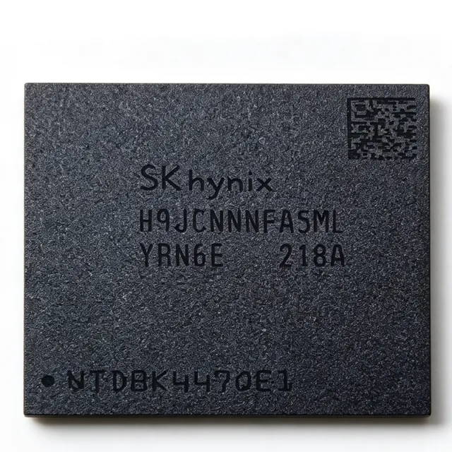
K3LKBKB0BM-MGCP - 32Gbit LPDDR5 DRAM 6400Mbps | Samsung
MPN: K3LKBKB0BM-MGCP ✓ Active| Qty | Unit Price | Extended |
|---|---|---|
| 1 | $58.28 | $58.28 |
| 10 | $55.37 | $553.70 |
| 100 | $52.45 | $5,245.00 |
| 500 | $49.53 | $24,765.00 |
| 1,000 | $46.62 | $46,620.00 |
K3LKBKB0BM-MGCP Overview
LPDDR5 (Low Power Double Data Rate 5) is the fifth generation of JEDEC low-power synchronous DRAM, a class of volatile memory that stores working data for application processors and SoCs. Within the memory hierarchy, LPDDR5 sits under the broader DRAM family alongside DDR4/DDR5, but is optimized for bandwidth-per-watt in battery-powered and thermally constrained systems rather than raw module capacity.
Key differentiating specifications include the 6400 Mbps/pin data rate, which doubles effective LPDDR4X-class bandwidth in comparable channel conditions; a 32 Gbit single-die density that allows 4 GB of memory in one package with a x32 I/O interface; and multi-rail operation (VDD1 1.05 V class core, VDD2 0.9 V class, VDDQ 0.5 V class, VDD2H 1.8 V class per the distributor listing) that reduces dynamic and standby power. The -25C to +85C operating window extends beyond the standard mobile range, supporting industrial controllers and outdoor connected devices.
Technically, the device belongs to Samsung's LPDDR5 family, which uses deep-sleep states, bank-group architecture, and dynamic voltage frequency scaling to cut idle power dramatically versus LPDDR4. Speed-class grading (this part is listed alongside LPDDR5-5500/6400 class material in web listings) allows platform designers to match memory bandwidth to SoC controller capability. Signal integrity at 6400 Mbps requires careful length-matched routing and reference-plane discipline on the PCB.
Typical applications include flagship smartphones and tablets, AI edge-compute modules, automotive infotainment SoCs, networking appliances, and industrial computing modules where 4 GB LPDDR5 density and low standby power are required.
Design consideration: at 6400 Mbps, routing and power-delivery design dominate system margins; use fly-by topology guidance from the Samsung LPDDR5 datasheet and validate the design at the corner data rates during SI/PI sign-off.
This page synthesizes distributor pricing, stock availability, drop-in alternative guidance, and practical design notes not found in the manufacturer datasheet alone.
Drop-in alternatives for K3LKBKB0BM-MGCP — same package, pin-to-pin compatible. Different-package parts requiring PCB rework are excluded.
Variants in this series
Same-series models that are drop-in compatible with K3LKBKB0BM-MGCP (same form factor and footprint) — differing in Package, Memory Type, Density, Interface, Application Class.
Quick Comparison Tool — Select alternative parts for side-by-side comparison:
K3LKCKB0BM-MGCP
📋 Reference alternative (not in catalog)
K3LKDKB0BM-MGCP
📋 Reference alternative (not in catalog)
K3LKBKB0BM-MGCP Maximum Ratings & Electrical Characteristics
| Memory Type | DRAM (LPDDR5 SDRAM) |
| Memory Size | 32 Gbit |
| Organization | 1G x 32 |
| Data Rate | 6400 Mbps per pin |
| Supply Voltage Rails | 500 mV, 900 mV, 1.05 V, 1.8 V |
| Interface | LPDDR5 x32 |
| Package | FBGA-315 |
| Mounting Type | Surface Mount |
| Operating Temperature | -25C to +85C |
| Technology Generation | LPDDR5 (JEDEC LPDDR5 family) |
| RoHS Status | Compliant |
| Density per Package | 4 GB (32 Gbit) |
| Refresh | Self-refresh and auto-refresh (LPDDR5 standard) |
| Application Segment | Mobile, embedded, industrial computing |
| Standby / Deep Sleep | LPDDR5 deep-sleep power states |
K3LKBKB0BM-MGCP 4 gb (32 gbit) Pin Configuration Guide
Pin configuration for K3LKBKB0BM-MGCP (4 gb (32 gbit) package). This digital IC includes GPIO, communication interfaces (UART, SPI, I2C), and power pins. Refer to the manufacturer datasheet for alternate pin functions and configuration options. Essential for embedded system design and PCB layout.

No detailed pinout data available for K3LKBKB0BM-MGCP.
Refer to the datasheet for full pin configuration.
Typical Applications
K3LKBKB0BM-MGCP is suitable for 6 applications: Flagship Smartphone and Tablet Memory, AI Edge Compute Modules, Industrial Controllers and HMI, Networking and Gateway Appliances, Automotive Infotainment (Non-Safety), Test, Measurement and Compute Modules.
Flagship Smartphone and Tablet Memory
K3LKBKB0BM-MGCP fits flagship smartphone and tablet platforms that require 4 GB of main memory in a single package. Its 6400 Mbps x32 interface provides roughly 25.6 GB/s of peak single-package bandwidth, sufficient for large-app multitasking and on-device AI inference on mobile SoCs. The four-rail power architecture (500 mV, 900 mV, 1.05 V, 1.8 V) with LPDDR5 deep-sleep states reduces standby drain, directly extending battery life in always-on devices. Placement close to the application processor on a short, length-matched bus preserves signal integrity at the full data rate; the main trade-off is stricter PCB layer count and impedance control versus lower-speed LPDDR4X memory.
Recommended
AI Edge Compute Modules
Edge AI accelerators and compute modules benefit from K3LKBKB0BM-MGCP because model weights and activation buffers demand both capacity and bandwidth: one 32 Gbit package delivers 4 GB with about 25.6 GB/s peak bandwidth at 6400 Mbps, avoiding a second memory device on a crowded module. The x32 organization matches the 32-bit controllers common in edge AI SoCs. LPDDR5 deep-sleep modes keep idle power low in duty-cycled sensing applications. Designers should derate bandwidth for controller efficiency (typically 60-70% of peak) when sizing models, and must verify the -25C to +85C rating covers the module enclosure temperature near the memory die.
Recommended
Industrial Controllers and HMI
The K3LKBKB0BM-MGCP operating range of -25C to +85C exceeds standard mobile LPDDR5 grading, making it appropriate for industrial controllers, HMIs, and embedded logging systems exposed to cabinet temperature swings. One package supplies 4 GB for data logging, protocol buffers, and local analytics on industrial SoCs. The 6400 Mbps interface shortens memory access latency for real-time control loops relative to LPDDR4-class memory. Power design should sequence the 1.8 V, 1.05 V, 0.9 V, and 0.5 V rails per the Samsung datasheet to avoid latch-up during brownouts, and long-term supply agreements are recommended for multi-year industrial programs.
Recommended
Networking and Gateway Appliances
Networking gateways, routers, and NVR appliances use K3LKBKB0BM-MGCP where 4 GB of DRAM supports packet buffering, connection tracking, and edge caching on a single low-power device. The 6400 Mbps x32 interface supplies roughly 25.6 GB/s peak bandwidth, adequate for gigabit-class and entry multi-gigabit forwarding planes when paired with a capable SoC. Compared with DDR4 DIMM solutions, the LPDDR5 package saves board area and cuts standby power, which matters for always-on fanless gateways. Signal integrity at the full data rate requires careful fly-by routing and reference-plane continuity; many gateway designs derate the memory clock to gain routing margin.
Recommended
Automotive Infotainment (Non-Safety)
Automotive infotainment and cockpit SoCs that accept LPDDR5 can use K3LKBKB0BM-MGCP for display graphics, navigation, and media buffering, where 4 GB per package and 6400 Mbps bandwidth support multi-display clusters. The extended -25C rating covers many cabin electronics mounting locations. Note this exact MPN is not verified as AEC-Q100 qualified in the available data, so it should be confined to non-safety, non-critical cockpit functions or to platforms where the Samsung automotive-qualified LPDDR5 variant is selected instead. Rail sequencing and self-refresh behavior during vehicle power modes (accessory, crank, sleep) must follow the Samsung LPDDR5 power-state table.
Recommended
Test, Measurement and Compute Modules
Instrumentation and SoM (system-on-module) builders adopt K3LKBKB0BM-MGCP to give modular compute boards 4 GB of fast, low-power memory within a small footprint. The single-package 32 Gbit density simplifies BOM logistics compared with stacking two lower-density devices, and the 6400 Mbps interface keeps captured waveform buffers and logging throughput high. Because SoM carriers vary in routing length, module designers should characterize memory margins across the -25C to +85C range and across speed-bin corners before locking the carrier-board design. The LPDDR5 deep-sleep states also benefit battery-backed portable instruments that duty-cycle compute between measurements.
Recommended
Recommended Products Summary
Engineering reference data for K3LKBKB0BM-MGCP — comparison, design guidance, and compliance information.
Selection Guide
Comparison with Alternatives
| Parameter | This Product | K3LKCKB0BM-MGCP | K3LKDKB0BM-MGCP |
|---|---|---|---|
| Package | FBGA (LPDDR5, x32) | FBGA (LPDDR5, x32) | FBGA (LPDDR5, x32) |
| Brand | Samsung Electronics | Samsung Electronics | Samsung Electronics |
| Memory Density | 32 Gbit (4 GB) | 16 Gbit (2 GB) | 32 Gbit (4 GB) |
| Interface | LPDDR5 x32 | LPDDR5 x32 | LPDDR5 x32 |
| Supply Rails | 500 mV / 900 mV / 1.05 V / 1.8 V | LPDDR5 standard rails | LPDDR5 standard rails |
| Package Capacity per Device | 4 GB | 2 GB | 4 GB |
Key Differentiators
- Highest density in single package (vs K3LKCKB0BM-MGCP)
- Extended temperature range (vs K3LKDKB0BM-MGCP)
- Trade-off: no verified cross-brand drop-in (vs SK Hynix / Micron LPDDR5 equivalents)
Design Notes
K3LKBKB0BM-MGCP uses four supply rails: 500 mV, 900 mV, 1.05 V, and 1.8 V. Sequence and decouple each rail per the Samsung LPDDR5 power-up procedure; a common LPDDR5 pitfall is powering VDDQ (0.5 V class) before the core rail, which can violate input safety constraints. Budget current from the datasheet IDD tables at the 6400 Mbps bin rather than typical LPDDR4 figures, and add at least 10-22 uF of bulk plus local 0.1 uF ceramic decoupling per rail group close to the balls.
At 6400 Mbps per pin, the CA and DQ bus behaves as a high-speed serial-like channel: keep trace stubs under 0.5 mm, length-match within the datasheet skew budget, and maintain continuous reference planes under the memory fly-by routing. Avoid routing LPDDR5 signals across plane splits, and simulate the channel at corner data rates before tape-out. Many designs derate to a lower LPDDR5 speed bin to recover SI margin on long module-to-carrier paths; confirm the derated bin is supported by the SoC controller.
Do not assume pin compatibility with LPDDR4X parts such as K4RBH046VM or third-party LPDDR5 vendors: FBGA ballmaps are vendor- and generation-specific, so footprint reuse requires direct ballmap comparison against the Samsung datasheet. Also note the verified temperature range is -25C to +85C, not the full -40C industrial range; designs exposed below -25C need an in-situ heater strategy or a wider-range qualified part. Finally, ZQ calibration resistor placement and value must follow the Samsung reference layout.
Compliance Information
RoHS compliance stated in JLCPCB listing. REACH, lead-free, halogen-free, and conflict-minerals declarations not stated in verified data for this exact MPN; request material declaration from Samsung.



