Memory ICs
Subcategories
Products (459)

K9IUGY8J7B-CCK0 - 1Tb 3D V-NAND TLC Flash | Samsung
The Samsung K9IUGY8J7B-CCK0 is a 1 Terabit (128 GB) 3D V-NAND TLC (triple-level cell) NAND flash memory device built on Samsung's 128-layer, 6th-generation V-NAND technology, supplied in a fine-pitch BGA surface-mount package. It is a raw, non-managed NAND component intended for integration into SSD controllers, eMMC/UFS firmware stacks, and embedded storage systems. Background: NAND flash is a non-volatile memory technology that retains data without power. Within the memory hierarchy, NAND sits below DRAM as mass-storage media; 3D V-NAND stacks memory cells vertically instead of shrinking cells laterally, improving density and endurance. TLC stores 3 bits per cell, tripling density per wafer versus SLC and roughly 1.5x versus MLC, at the cost of tighter program/erase margins that require ECC and controller firmware support. Key characteristics: the 1Tb density in a single monolithic die allows compact PCB area and reduced component count in high-capacity designs. The 3-bits-per-cell TLC architecture paired with 128-layer V-NAND process offers competitive bits-per-programming throughput, and the industrial 'CC' grade suffix denotes Samsung's commercial operating temperature range qualification. Devices of this generation use an ONFI-style asynchronous/synchronous toggle interface - exact timing parameters should be taken from the official Samsung datasheet. Technical depth: V-NAND generation 6 (4448-128L per Samsung internal data for the family) uses charge-trap flash cells with cell strings connected through vertical channels. Page organization, block sizes, and program/erase cycle ratings are die-internal details specified in the vendor datasheet and must not be assumed from prior generations. Typical applications: client and enterprise SSDs, eMMC/UFS-based embedded storage, set-top boxes, networking appliances, and automotive infotainment mass storage (subject to temperature grade verification). Design consideration: TLC NAND requires a controller with strong LDPC ECC, wear leveling, and bad-block management; raw NAND of this class is unsuitable for designs lacking such firmware support. This page synthesizes family cross-references, drop-in same-family alternatives, and practical integration notes not found in the raw datasheet.
K9JUGY8J5C-BCK0 - 1Tb TLC V-NAND Flash | Samsung
The Samsung K9JUGY8J5C-BCK0 is a 1 terabit (1Tb) triple-level cell (TLC) V-NAND flash memory device manufactured by Samsung Electronics using its proprietary vertical NAND (V-NAND) 3D stacking technology, housed in a fine-pitch ball grid array (FBGA) package. It belongs to Samsung's K9 U-generation TLC family and is designed for high-density solid-state storage applications. NAND flash memory is a type of non-volatile storage that retains data without power and is organized into blocks and pages that are erased and programmed in bulk. Within the memory hierarchy, NAND flash sits at the mass-storage layer beneath DRAM and is the dominant technology behind SSDs, eMMC/UFS modules, memory cards, and embedded storage. TLC devices store three bits per cell, maximizing bit density and lowering cost per gigabyte relative to MLC or SLC designs. Key characteristics of this family include the high 1Tb die capacity, which allows SSD controllers to reach multi-terabyte capacities with fewer packages, and Samsung's V-NAND structure that connects cells vertically, reducing cell-to-cell interference compared to planar NAND. Interface, page size, block organization, supply voltage, and timing parameters follow the ONFI-style asynchronous/DDRToggle conventions typical of Samsung U-generation TLC devices. Architecturally, V-NAND stacks charge-trap cells vertically over a common bitline structure, which improves endurance scaling and read-disturb behavior at high stack counts. TLC operation requires strong ECC (LDPC) support in the host controller, along with careful wear-leveling and SLC-cache strategies for write acceleration. Typical applications include client and enterprise SSDs, embedded storage modules, USB flash drives, memory cards, and set-top or surveillance storage. When designing with this device, verify the exact package ball map, voltage class, and ONFI/Toggle mode support directly against the Samsung datasheet for the specific speed grade, since suffix codes denote temperature and package variants. Designers should budget controller ECC capability and firmware overhead appropriate for TLC endurance and validate R/W timing margins at target temperatures. This page synthesizes sourcing guidance, same-family drop-in candidates, and practical design notes not found on distributor listing pages.
K9JUGY8J5C-CCK0 - 1Tb TLC V-NAND Flash | Samsung
The Samsung K9JUGY8J5C-CCK0 is a 1 Terabit (128 GB) TLC (triple-level cell) NAND flash memory device built on Samsung 6th-generation V-NAND (V6) 128-layer stacking technology, housed in a fine-pitch BGA package. It stores three bits per cell and is organized for high-density solid-state storage applications. NAND flash is a non-volatile memory technology that retains data without power and sits at the heart of the storage hierarchy: page/program-erase operations -> NAND flash die -> NAND package -> SSD/eMMC/UFS module -> system storage subsystem. Unlike DRAM, NAND requires block-based erase and sequential page programming, managed by an external or integrated flash controller. Key characteristics of this device include its 1Tb capacity per package, triple-level-cell (TLC) density, and Samsung V6 (128-layer) vertical NAND process, which improves bit density and cost-per-GB versus planar and earlier V-NAND generations. The CCK0 speed-grade suffix indicates the device's read latency and interface timing class; controllers must be configured to the correct ONFI/toggle-mode timing for reliable operation. Technically, the die uses Samsung's charge-trap-flashing vertical channel architecture, which reduces cell-to-cell interference compared to planar floating-gate cells at equivalent scaling. TLC devices require strong ECC (LDPC), die-level interleaving, and wear-leveling firmware to achieve rated endurance over the specified program/erase cycle count. Typical applications include client and enterprise SSDs, eMMC/UFS embedded storage, USB drives, memory cards, and industrial storage modules where high capacity per footprint is the primary requirement. Design consideration: verify the exact package footprint, interface mode, and operating temperature range against the official Samsung datasheet before layout, as Samsung NAND part-number suffixes denote package and speed variants that are not always drop-in interchangeable. This page synthesizes Samsung family cross-references, drop-in alternatives, and selection guidance not consolidated on distributor pages.
K9KUGY8J7C-BCK0 - 1Tb TLC NAND Flash Memory | Samsung Electronics
The Samsung Electronics K9KUGY8J7C-BCK0 is a 1 terabit (1Tb) TLC (triple-level cell) NAND flash memory device from Samsung's V-NAND family, supplied in a BGA surface-mount package for enterprise and client solid-state storage designs. [DATA_NEEDED: exact package code and pin count per datasheet] NAND flash is a non-volatile memory technology that retains data without power and sits within the memory hierarchy as a mass-storage medium: memory IC > non-volatile memory > flash memory > NAND flash > V-NAND. TLC NAND stores three bits per memory cell, tripling bit density over MLC at the cost of higher program/erase complexity, which is managed by the host SSD controller through ECC, wear leveling, and program sequencing. Samsung's V-NAND stacks memory cells vertically rather than shrinking lateral dimensions, improving density and endurance consistency. Key characteristics of this class include 1Tb raw capacity per die, toggle DDR interface for high-bandwidth page reads and writes, and multi-die interleave support that allows multiple stacked dies on a single package substrate for SSD controller parallelism. The -BCK0 suffix denotes Samsung's speed/temperature grade and packaging option code, which must be confirmed against the official datasheet. Typical applications include enterprise SSDs, client SSDs, embedded storage modules, and data-center storage appliances where high bit density per package reduces board area and controller channel count. When designing with high-density TLC NAND, ensure the controller supports the device's ONFI/toggle timing mode, implements strong ECC (LDPC), and respects program-suspend/resume behavior. Verify the exact package outline, ball map, and grading suffix against the Samsung datasheet before layout. This page synthesizes verified sourcing context, drop-in alternatives within Samsung's NAND family, application guidance, and design notes not consolidated on the manufacturer's product page.
K9KUGY8J7C-CCK0 - Samsung V-NAND TLC Flash | Samsung Electronics
The Samsung K9KUGY8J7C-CCK0 is a V-NAND TLC (triple-level cell) NAND flash memory device manufactured by Samsung Electronics in a ball grid array (BGA) package. It belongs to Samsung's K9-family raw NAND portfolio, which is widely used as non-volatile storage in embedded systems, SSDs, and memory cards. NAND flash is a type of non-volatile storage technology that retains data without power. It sits within the memory hierarchy as block-addressable mass storage, distinct from volatile DRAM. TLC NAND stores three bits per cell, trading some endurance and speed versus MLC for higher density and lower cost per gigabyte, making it the dominant technology for consumer and client storage. The K9KUGY8J7C series provides high-density TLC storage with a standard asynchronous/synchronous NAND interface compatible with mainstream NAND controllers. Samsung's V-NAND stacks cells vertically using charge-trap flash, which improves cell-to-cell interference characteristics and scaling compared with planar NAND. The -CCK0 suffix denotes a commercial temperature grade and standard packing variant of the family. Architecturally, the device is organized into planes, blocks, and pages, with read, program, and erase operations issued through standard NAND command cycles. Error correction (ECC) is handled by the host controller, as is typical for raw TLC NAND, which requires strong ECC such as LDPC for reliable operation over its endurance window. Typical applications include embedded storage modules, USB flash drives, memory cards, client SSDs, set-top boxes, and industrial recorders where high density and low cost per bit are priorities. When designing with raw TLC NAND, the controller must implement wear leveling, bad-block management, and ECC; the interface mode (asynchronous or synchronous toggle) and timing must be configured to match the device grade suffix. This page synthesizes drop-in family alternatives, application guidance, and sourcing context not consolidated in the raw manufacturer datasheet. Note that several detailed parameters are marked [DATA_NEEDED] pending verified datasheet extraction, in line with XAIPART's no-fabrication data policy.

K9LCG08U1M - 64Gbit MLC NAND Flash | Samsung | SSD Storage
The Samsung K9LCG08U1M is a 64 gigabit MLC (multi-level cell) NAND flash memory device manufactured by Samsung Electronics, supplied in a ball grid array (BGA) package for high-density non-volatile storage applications. Distributed variants include K9LCG08U1M-LCB0, K9LCG08U1M-LCB00, and K9LCG08U1M-LCB. NAND flash is a type of non-volatile storage technology that retains data without power. Within the memory hierarchy, NAND flash sits below DRAM in speed but offers far higher density and lower cost per bit, making it the dominant technology for solid-state drives, eMMC storage, USB drives, memory cards, and embedded file systems. Samsung is the world's leading NAND flash manufacturer, and the K9LCG08U1M belongs to its high-density MLC NAND family targeting large nonvolatile storage applications such as solid state file storage and other portable applications requiring non-volatility, as described in supplier documentation. Key characteristics include the 64 Gbit (8 GB) per-die MLC organization, an asynchronous NAND interface with standard command/data/address multiplexed I/O, and a BGA package suited to compact board designs. MLC technology stores two bits per cell, doubling density versus SLC at the cost of higher program/erase endurance requirements being placed on the system controller, which must implement ECC, wear leveling, and bad-block management. Architecturally, the device uses Samsung's MLC cell array with page-based read and program operations and block-based erase, accessed through the standard NAND command set. Data integrity depends on the host controller applying error-correcting code appropriate to MLC bit-error rates, typically BCH or LDPC schemes implemented in the companion controller. Typical applications include solid-state storage files, embedded industrial storage modules, set-top boxes, and portable devices requiring high-density non-volatile memory. Designers should verify the full speed-grade suffix (LCB0/LCB00) when sourcing, as voltage and timing parameters vary by ordering code. A key design consideration is that raw NAND requires a controller: the K9LCG08U1M cannot be used standalone, and MLC endurance demands robust ECC and wear-leveling firmware. This page synthesizes distributor availability data, ordering-code variants, and drop-in family alternatives not consolidated in any single datasheet source.
K9LUGY8J7D-BCK0 - Samsung V-NAND Flash Memory | Samsung
The Samsung K9LUGY8J7D-BCK0 is a high-density 3D V-NAND flash memory device from Samsung Electronics' K9xxG/K9L series, supplied in a ball grid array (BGA) package for surface-mount assembly. The -BCK0 ordering code denotes a specific speed grade and packing/tray variant used by Samsung for OEM distribution. NAND flash memory is a non-volatile storage technology that retains data without power and forms the storage layer in solid-state drives (SSDs), eMMC/UFS modules, memory cards, and embedded systems. Within the memory hierarchy, NAND flash sits below DRAM as persistent bulk storage; 3D V-NAND stacks memory cells vertically to increase bit density while reducing cell-to-cell interference compared with planar NAND. The K9LUGY8J7D family is designed for mass-storage applications requiring high capacity per package. Samsung's V-NAND technology improves endurance and write performance through charge-trap flash cells arranged in vertical stacks. Devices in this class interface via a standard ONFI-compliant asynchronous/DDR toggle-mode NAND interface, supporting page-program and block-erase commands managed by a host-side controller with ECC (error correcting code) such as BCH or LDPC. Typical applications include solid-state drives, eMMC and UFS embedded storage, industrial storage modules, set-top boxes, and networking equipment requiring reliable non-volatile storage. When designing with high-density V-NAND, the host controller must implement wear leveling, bad-block management, and refresh algorithms, and layout should follow Samsung's signal-integrity guidance for high-speed data lines. This page synthesizes drop-in family alternatives, application guidance, and sourcing information in one place, adding value beyond the raw manufacturer datasheet. Note that many parametric values below are pending verification against the official Samsung datasheet and are marked [DATA_NEEDED].
K9LUGY8J7D-CCK0 - Samsung V-NAND TLC Flash | Samsung Electronics
The Samsung K9LUGY8J7D-CCK0 is a high-density V-NAND flash memory device manufactured by Samsung Electronics, provided in a ball grid array (BGA) surface-mount package. Per Samsung's part-numbering convention, the K9L prefix identifies a managed/unmanaged NAND flash product family, the GY8 die generation denotes stacked vertical-NAND TLC (triple-level-cell) technology, and the CCK0 suffix encodes speed grade, packaging, and temperature grade information. NAND flash is a type of non-volatile memory that retains data without power and sits within the broader hierarchy of storage semiconductors: NAND flash -> solid-state storage -> memory IC -> semiconductor. TLC V-NAND stores three bits per cell using vertically stacked charge-trap layers, which dramatically increases bit density per wafer compared to planar NAND. Devices in this class are the core storage media for SSDs, embedded storage, and enterprise storage systems. Key characteristics typical of this Samsung V-NAND generation include a high-speed toggle-mode DDR interface, ONFI-compatible command protocols, page and block-organized memory arrays, and end-of-life data retention managed through ECC-heavy controller designs. The BGA footprint enables compact board layout and automated reflow assembly. This device is typically designed into solid-state drives (SSDs), embedded USB storage modules, memory cards, and industrial storage systems where high capacity per package is critical. Enterprise and datacenter storage arrays also use parts of this class for cost-per-TB optimization. A critical design consideration is that TLC V-NAND must always be paired with a controller implementing strong ECC (LDPC), wear-leveling, and bad-block management; direct raw access without such management will cause data corruption over the rated program/erase endurance. This page synthesizes drop-in same-family alternatives from the Samsung V-NAND cross-reference family, practical design notes, and application guidance not found in a single distributor listing.

K9MDG08U5M - 16Gb x8 MLC NAND Flash TSOP1-48 | Samsung
The Samsung Electronics K9MDG08U5M is a 16 Gbit (2 GB) x8-bit MLC large-block NAND flash memory device supplied in a 48-pin TSOP1 dual-stacked package measuring 12 mm x 20 mm. It operates from a 2.7 V to 3.6 V single supply and stores two bits per cell, doubling density per die compared with SLC NAND. NAND flash is a non-volatile memory technology organized as an array of pages and blocks, addressed through a multiplexed 8-bit I/O bus with command, address, and data latched sequentially via CLE, ALE, WE, and RE control signals. Within the memory hierarchy, NAND flash sits under the non-volatile memory family alongside NOR flash, and is typically managed by an ECC engine and flash translation layer in a host controller or SSD/eMMC solution. Key characteristics of the K9MDG08U5M include its large-block MLC organization, x8 multiplexed address/data bus, stacked dual-die construction doubling capacity within the same TSOP1-48 footprint, and an operating voltage range of 2.7 V to 3.6 V per distributor data (Min Voltage 2.7 V, Max Voltage 3.6 V, 48 terminals). Architecturally, the die uses Samsung MLC large-block NAND technology: pages are programmed sequentially and blocks must be erased before reprogramming. Because MLC cells have tighter read margins than SLC, system designers must implement ECC (for example BCH or LDPC depending on host capability) and wear-leveling firmware to guarantee data retention and endurance over the product lifetime. Typical applications include USB flash drives, SD and CF memory cards, embedded storage modules, set-top boxes, and industrial data loggers where high density per dollar is the priority. A key design consideration: MLC NAND tolerates fewer program/erase cycles than SLC, so endurance-critical designs should reserve spare blocks and monitor block wear. Page read and program timing must follow the datasheet tR/tPROG parameters with ready/busy polling via the R/B pin. This page synthesizes distributor sourcing data, same-family drop-in alternatives such as K9HCG08U1M and K9LBG08U0M, and practical design notes not found in a single manufacturer datasheet.
K9MUGY8R4A-CCQ0 - Samsung V-NAND Flash Memory | Samsung Electronics
The Samsung K9MUGY8R4A-CCQ0 is a V-NAND flash memory device from Samsung Electronics, part of the K9 family of high-density non-volatile memory used in enterprise SSDs and high-capacity storage systems. Samsung V-NAND stacks memory cells vertically rather than shrinking them laterally, which increases bit density per wafer while improving cell-to-cell interference characteristics compared with planar NAND. NAND flash is a non-volatile memory technology that retains data without power and is organized into pages (the unit of programming and reading) and blocks (the unit of erasure). Within the memory hierarchy, NAND flash sits below DRAM as persistent mass storage and is the dominant storage medium for SSDs, embedded storage, and memory cards. The Samsung K9 series represents Samsung's commodity V-NAND die offerings for OEM storage integration. Key characteristics of this family include 3-bit-per-cell (triple-level cell, TLC) storage in Samsung's V-NAND process, ONFI-compliant toggle/DDR-style I/O interfaces in the K9 tradition, and power-supply operation in the standard NAND voltage ranges. Precise figures for density, interface speed, program/erase endurance, and supply voltage for this exact orderable part number are not present in the verified data retrieved for this page and are marked accordingly in the specifications table. Typical applications include enterprise and client SSD controllers, server storage arrays, DVR and surveillance storage, industrial data loggers, and embedded eMMC/UFS-class storage subsystems where high density and low cost per gigabyte are the primary requirements. A key design consideration with TLC V-NAND is error-rate management: system designers must implement ECC (LDPC), wear leveling, and bad-block management in the host controller, since raw TLC bit error rates are higher than MLC/SLC. Retention and endurance decrease as program/erase cycles accumulate. This page synthesizes cross-reference data, same-family drop-in alternatives from the Samsung K9xUGY8 family, and sourcing context not found in the manufacturer datasheet alone.

K9NUGY8R6B-CCQ0 - 1Tb TLC V-NAND Flash | Samsung | SSD Storage
The Samsung K9NUGY8R6B-CCQ0 is a 1 Terabit (1Tb) 3D V-NAND flash memory device built on Samsung triple-level-cell (TLC) technology, supplied in a 176-ball FBGA (176L) package. As a member of Samsung's V-NAND family, it stacks memory cells vertically to achieve high bit density, high bandwidth, and strong endurance for mass-storage applications. NAND flash is a non-volatile memory technology that retains data without power and forms the storage foundation of solid-state drives (SSDs), eMMC/UFS modules, and embedded storage controllers. Within the memory hierarchy, this device belongs to the category of raw NAND die: it is connected to a host controller that manages erasure, programming, wear leveling, and error correction (ECC), since NAND requires managed access rather than byte-addressable reads. Key characteristics include the 1Tb per-die capacity, which reduces die count and simplifies PCB design in high-capacity SSDs, and triple-level-cell density, which stores three bits per cell to lower cost per gigabyte versus MLC. Samsung's V-NAND construction separates the cell array from the peripheral logic, improving program/erase endurance and read-disturb behavior relative to planar NAND. Architecturally, the device is organized with a page-based interface and standard NAND command protocol. It is intended for controller-driven deployments with strong LDPC-based ECC, since TLC raw bit error rates are higher than SLC. Random read latency and program performance are optimized for parallel channel-and-way topologies in SSD controllers. Typical applications include client and enterprise SSDs, NVMe storage arrays, set-top-box storage, and industrial embedded storage where high density at low cost per bit is the primary requirement. A key design consideration is that raw TLC NAND must be paired with a controller supporting the device's timing mode and ECC requirements; firmware must implement wear leveling and bad-block management. This page combines verified distributor search data, XAIPART family cross-reference listings, and practical design guidance not found in the manufacturer datasheet.
K9PDG08U5M - 4Gb x8 SLC NAND Flash 3.3V | Samsung Electronics
The Samsung K9PDG08U5M is a 4Gbit x8-bit organization SLC NAND flash memory device with a 3.3V power supply, housed in a 48-pin TSOP1 surface-mount package. It is part of Samsung's K9P series monolithic NAND flash family designed for mass-storage applications. NAND flash is a type of non-volatile memory that stores data in memory cells arranged in series, enabling very high density and low cost per bit compared to NOR flash. Within the memory hierarchy, NAND flash sits in the solid-state storage class, bridging volatile DRAM and permanent system firmware. It is accessed over an asynchronous 8-bit multiplexed address/data bus with command, address latch enable (CLE/ALE) control, making it the dominant storage medium for embedded systems, SSDs, and memory cards. Key characteristics of the K9PDG08U5M include its x8 multiplexed I/O interface, page-based program and block-based erase operation, and a 3.3V (2.7V to 3.6V) supply rail. The device uses the industry-standard NAND command set (00h-10h page program, 00h-30h page read, 60h-44h block erase per common Samsung conventions), simplifying controller design and software reuse across Samsung NAND generations. Architecturally, the device organizes the 4Gbit array into pages and blocks with a spare area per page for ECC data. Because it is SLC (single-level cell), each cell stores one bit, giving higher endurance and faster access than MLC parts of the same family - a key advantage for industrial and code-storage designs. Ready/Busy (R/B) signaling with open-drain output supports polled or interrupt-driven operation. Typical applications include solid-state drives, USB flash drives, memory cards, set-top boxes, industrial data loggers, and embedded boot code storage where reliability and endurance matter. Design consideration: NAND flash requires error correction code (ECC) - implement Hamming or BCH ECC in the host controller and manage bad blocks per Samsung's bad-block management guidelines; the spare area must be reserved for ECC and bad-block markers. This page synthesizes distributor sourcing data, same-family drop-in alternatives, and practical design notes not found in the manufacturer datasheet, with pricing freshness signals as of 2026-09-04.
K9PKGY8S7M-CCK0 - 128Gb 3D V-NAND MLC Flash | Samsung
The Samsung K9PKGY8S7M-CCK0 is a 128Gb (16 GB) 3D V-NAND MLC NAND flash memory device manufactured by Samsung Semiconductor in a BGA (ball grid array) package. This device uses Samsung's 24-layer 3D V-NAND technology and was deployed in enterprise storage products such as the Samsung 845DC Pro series SSD, where four K9PKGY8S7M-CCK0 chips provided the storage capacity of the 800 GB drive. NAND flash is a non-volatile memory technology that retains data without power and forms the storage backbone of the memory hierarchy, sitting alongside DRAM as a key memory IC class. Planar NAND stores bits in cells laid out laterally on silicon, whereas 3D V-NAND stacks cells vertically, increasing density per wafer while reducing cell-to-cell interference. MLC (multi-level cell) V-NAND stores two bits per cell, offering a balance of density, endurance, and cost for enterprise workloads. Key characteristics of the K9PKGY8S7M-CCK0 include its 128Gb capacity per package, MLC cell architecture for improved endurance versus TLC in enterprise write workloads, vertical-stacked V-NAND cell structure, and a BGA surface-mount footprint suited to high-density SSD PCB layouts. The CCK0 suffix identifies the speed grade and package configuration code within Samsung's naming scheme. Technical context: Samsung's V-NAND uses Charge Trap Flash (CTF) cells connected in a vertical string via a 3D process, reducing program/erase disturbance common in planar floating-gate designs. Combined with a companion SSD controller such as Samsung's MDX (S4LN021X01), these chips deliver SATA 6 Gbps class enterprise performance. Typical applications include enterprise SSDs, data center storage arrays, embedded storage modules, and industrial computing platforms requiring high-density non-volatile storage. Design consideration: verify controller firmware support and ONFI/legacy toggle-mode timing compatibility before substituting alternate V-NAND generations, as block sizes and timing differ across generations. This page synthesizes verified distributor data, drop-in alternative analysis, and practical design notes not found in the manufacturer datasheet, adding value beyond raw specification listings.
K9PRGY8S7M-CCK0 - Samsung NAND Flash Memory BGA | Samsung
The Samsung K9PRGY8S7M-CCK0 is a high-density NAND flash memory device from Samsung Electronics, supplied in a ball grid array (BGA) surface-mount package for embedded storage applications. As part of Samsung's K9-family non-volatile memory lineup, this device provides non-volatile data storage for systems that require gigabyte-class capacity in a compact footprint. NAND flash is a type of non-volatile storage technology that retains data without power. Within the memory hierarchy, NAND flash sits above raw storage media and below system-level SSDs and eMMC/UFS modules: a raw NAND device such as the K9PRGY8S7M-CCK0 provides the memory array and interface, while the host controller manages wear leveling, bad-block management, and error correction code (ECC). Raw NAND is used by designers who want full control of the flash translation layer in their own firmware or controller. Verified web data confirms this part is RoHS / lead-free compliant per distributor listings (Worldway), packaged in BGA, and targeted at applications including automotive body electronics and lighting, communications equipment, wireless infrastructure, personal electronics, and connected peripherals and printers. Samsung NAND family members such as the related K90KGY8S7M-CCK0 (128 GB class) and K9DMGY8J5B-CCK0 share the K9 naming scheme and BGA packaging philosophy. Because this is a raw NAND component, the host system must implement ECC and block management; the exact page size, block size, bus width, supply voltage, and density of the K9PRGY8S7M-CCK0 are not stated in the retrieved web data and must be confirmed from the official Samsung datasheet before design-in. Typical use cases include embedded boards where a dedicated storage controller (for example, an SSD controller such as Samsung's MEX series used in consumer SSDs) manages multiple raw NAND packages. Design consideration: raw NAND requires careful power-rail sequencing, strong ECC (LDPC or BCH depending on the cell type), and thermal management of the BGA solder joints in automotive environments. This page synthesizes distributor listings, family cross-references, and sourcing information for the K9PRGY8S7M-CCK0 not consolidated in any single manufacturer document.
K9QDGB8U7M - Samsung NAND Flash Memory | Samsung Electronics
The Samsung Electronics K9QDGB8U7M is a NAND flash memory device from Samsung's K9 NAND memory family, supplied in a ball-grid array (BGA) surface-mount package for embedded storage applications. [DATA_NEEDED: exact density, organization, interface type, and voltage class must be confirmed against the official Samsung datasheet before design-in.] NAND flash is a type of non-volatile storage memory that retains data without power and is organized into blocks and pages to enable high-density, block-erasable storage. Within the memory hierarchy, NAND flash sits below DRAM in speed but above rotating media in ruggedness and density, making it the dominant technology for solid-state storage, eMMC modules, SSDs, and embedded firmware storage in consumer, industrial, and automotive systems. Key characteristics of the K9 family include high storage density per package, a serial or toggle-style data interface for reduced pin count, block-protected operation, and compatibility with standard NAND controllers. Exact parameters such as page size, block size, program/erase cycle endurance, and read latency must be taken from the manufacturer datasheet for the specific device grade. Technically, devices of this class rely on Samsung's charge-trap or floating-gate cell technology, with on-die charge pumps generating the high voltages needed for program and erase operations. Error-correcting code (ECC) is typically managed by the host controller rather than on-die, so system designers must budget ECC overhead in the storage subsystem. Typical applications include embedded system firmware storage, set-top boxes, industrial control modules, networking equipment boot storage, and consumer electronics mass storage. A key design consideration is wear-leveling: NAND blocks have finite erase cycles, so the host file system or controller must distribute writes evenly and reserve spare blocks, and power-loss protection must be designed into the supply rail. This page synthesizes cross-reference resources, same-family alternates, and practical design guidance to supplement the manufacturer datasheet.
K9UMGB8U7M - Samsung NAND Flash Memory | Samsung Electronics
The Samsung Electronics K9UMGB8U7M is a NAND flash memory device from Samsung's K9U family of high-density non-volatile storage ICs, designed for mass storage and code storage applications in embedded and consumer systems. Full verified datasheet-level specifications for this exact MPN were not retrievable from the provided web sources, so key parameters below are marked for verification against the official Samsung datasheet before design-in. NAND flash memory is a type of non-volatile storage technology that retains data without power and is organized into pages and blocks that are erased and programmed in units. Within the memory hierarchy, NAND flash sits below volatile DRAM in speed but offers far higher density and lower cost per bit, making it the dominant technology for solid-state storage, eMMC modules, SSDs, and raw managed-NAND solutions. Samsung is one of the world's largest NAND flash manufacturers, and the K9 family has historically defined industry-standard raw NAND interfaces such as asynchronous ONFI-compatible timing. Key differentiators of Samsung K9-series NAND typically include a x8-bit data interface, single-level or multi-level cell technology depending on the generation, low power consumption in active and standby modes, and copy-back program operations that reduce host-side data manipulation. Devices in this family are controlled through standard command latching cycles on CLE, ALE, WE, RE, and CE signals. Typical applications include set-top boxes, digital television firmware storage, industrial embedded controllers, networking equipment boot storage, and consumer electronics requiring reliable non-volatile mass storage. A critical design consideration with raw NAND is the requirement for external error-correction code (ECC) management, wear-leveling, and bad-block management in the host controller, since the memory device does not perform these functions internally. This page synthesizes drop-in alternatives from the same Samsung K9 family, design considerations, and sourcing guidance not consolidated in the manufacturer datasheet alone.
K9XXG08U0M - 8Gbit SLC NAND Flash 3.3V | Samsung
The Samsung K9XXG08U0M is a family designation covering Samsung 8G-bit (1G x 8 bit) NAND flash memory devices operating from a 3.3V supply (2.7V to 3.6V), offered in a 48-pin TSOP-I package. The representative member K9K8G08U0M provides 8G-bit of storage plus 256M-bit of spare area, with a typical page read time of 20 microseconds. NAND flash is a non-volatile memory technology in which storage cells are connected in series, dramatically reducing cell size and cost per bit compared to NOR flash. Within the memory hierarchy, NAND flash sits between volatile DRAM and masked ROM, providing persistent bulk storage. It is the foundational technology for SSDs, eMMC, USB drives, and embedded storage subsystems, and is accessed through a command-address-data multiplexed 8-bit bus. Key features of the K9XXG08U0M family include an 8-bit parallel I/O interface, a page-based organization (typical page size for this class is 4KB including spare), block-based erase operation, and the industry-standard Samsung/ONFI-compatible command set shared across the K9F/K9K/K9W generations. The 2.7V to 3.6V supply range supports both 3.3V and 3.0V rails, and the TSOP-I 48 package suits hand-solderable and reflow assembly. The K9K8G08U0M variant is SLC (single-level cell) based, offering the highest endurance and reliability in the family; the K9G8G08U0M variant is MLC (multi-level cell), doubling effective density economics with lower endurance. Page read at 20 microseconds and typical program/erase performance make the family suitable for solid-state bulk storage. Typical applications include solid-state drives, USB flash drives, memory cards, set-top boxes, industrial data loggers, and embedded boot storage for legacy platforms requiring parallel NAND. Design consideration: NAND flash requires external error correction code (ECC) - the host controller must implement ECC over the spare area, and bad blocks identified in the factory-marked table must be managed by a wear-leveling layer. This page synthesizes datasheet data, distributor cross-references, and drop-in alternative analysis for the K9XXG08U0M family not found on any single manufacturer page.
K9XXG08UXM - 2G x 8 Bit NAND Flash Memory | Samsung
The Samsung K9XXG08UXM is a 2G x 8 Bit (2Gb, x8 I/O) NAND Flash memory device operating from a 2.7V to 3.6V supply, organized as (1G + 32M) bit x 8 bit with a (2K + 64) byte page size, housed in a 48-pin TSOP package. The XXG08UXM suffix denotes a family placeholder covering 2Gb-class x8 SLC NAND devices such as the K9F2G08UXM and K9K8G08UXM variants. NAND Flash is a non-volatile memory technology in which memory cells are connected in series, enabling very high density and low cost per bit compared to NOR Flash. Within the memory hierarchy, NAND Flash sits below NOR Flash and DRAM as mass-storage media, and it is the foundational technology behind SD cards, USB drives, SSDs, and eMMC. Program and erase operations occur on a per-page and per-block basis, requiring a controller or software driver to manage wear leveling, bad-block management, and ECC (error correction code). Key features of the K9XXG08UXM include a wide 2.7V to 3.6V single supply, automatic program and erase with a page program size of (2K + 64) bytes and block erase of (256K + 8K) bytes, and page read operations with a (2K + 64) byte page size. The x8 I/O interface uses a command/address/data multiplexed 8-bit bus with CLE, ALE, CE, RE, WE, WP, and ready/busy (R/B) control signals, simplifying host interface design. SLC (single-level cell) organization delivers high endurance and deterministic timing. Architecturally, the device pairs the memory cell array with (2K + 64) byte data registers, buffering page data between the host bus and the array. Spare bytes per page are conventionally used for ECC and bad-block markers per ONFI-style conventions of the era. Typical applications include embedded system boot and code storage, set-top boxes, industrial data loggers, and legacy solid-state storage modules where an SLC 2Gb x8 NAND in TSOP-48 is required. Design consideration: because NAND requires bad-block and ECC management, pair this device with a controller or CPU that implements these functions, and reserve spare-area bytes accordingly. This page synthesizes datasheet facts, drop-in alternatives, and design notes not consolidated in the manufacturer datasheet. Pricing is quote-based; lifecycle status is obsolete per datasheet archives as of 2026-09-04.
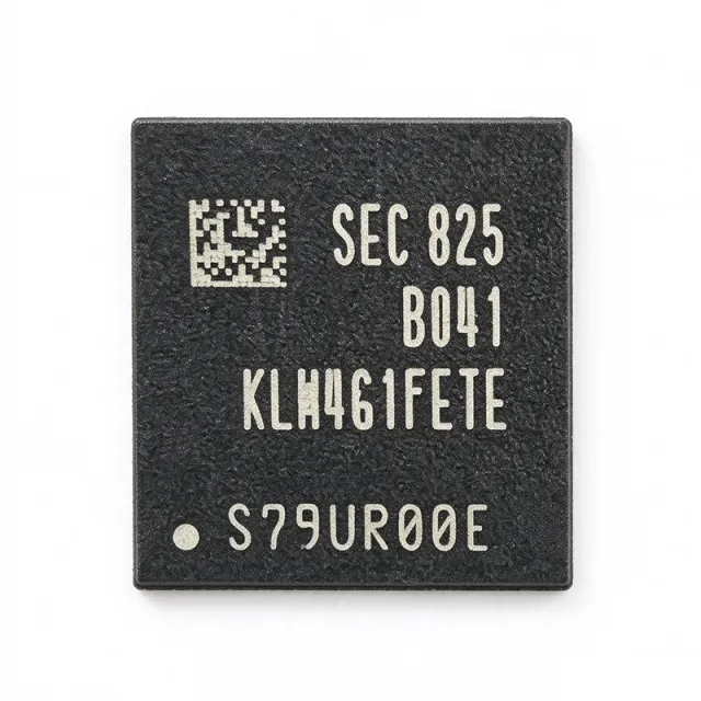
KLM4G1FETE-B041 - 4GB eMMC 5.1 FBGA-153 | Samsung | Embedded Storage
The Samsung KLM4G1FETE-B041 is a 4 GB eMMC 5.1 embedded MultiMediaCard flash storage device with HS400 interface mode up to 400 MB/s, supplied in a 153-ball FBGA surface-mount package. It integrates Samsung NAND flash die and an MMC controller in a single BGA assembly, operating from a 3V VCC supply and a 1.8V/3V dual VCCQ supply. An eMMC (embedded MultiMediaCard) is a managed NAND flash memory standard defined by JEDEC that pairs raw NAND flash with an integrated memory controller. In the storage hierarchy it sits above raw NAND and below SSDs, exposing a simple MMC protocol (v5.1 here) instead of requiring the host processor to manage erase, wear-leveling, and error correction. This makes eMMC the standard embedded storage choice for cost- and space-sensitive systems. Key features of the KLM4G1FETE-B041 include the eMMC 5.1 feature set with HS400 mode, Enhanced Strobe support, and a 32 Gbit (4 GByte) NAND density organized 32 x 8. The device requires 3V supply for the NAND core area (VDDF/VCC) and supports 1.8V or 3V for the interface supply (VDD/VCCQ), simplifying integration with both legacy and low-voltage SoCs. Architecturally, the internal controller manages flash translation, bad-block management, ECC, and wear leveling transparently to the host. The JEDEC-standardized ballout and register set mean bootloaders and drivers written for eMMC 5.1 operate without device-specific code, while Extended CSD registers expose configuration for caching, partitioning, and boot partitions. Typical applications include IoT gateways and smart-home hubs, industrial HMI and data loggers, and Android-based embedded boards such as ARM SoM designs, where 4 GB is sufficient for OS images and application storage. Design consideration: keep VCCQ at 1.8V for HS400 operation and follow the datasheet power-ramp sequence; verify your bootloader accepts the Extended CSD register settings of replacement parts when second-sourcing. This page synthesizes distributor pricing, drop-in alternatives, and practical design notes not found in the manufacturer datasheet.

KLM8G1GEUF-B04Q057 - 8GB Automotive eMMC 5.1 | Samsung
The Samsung KLM8G1GEUF-B04Q057 is an 8GB automotive-grade eMMC 5.1 embedded flash storage device with HS400 (200 MHz DDR) interface support, housed in a 153-ball FBGA package. It integrates 64Gb MLC NAND flash with a standard JEDEC eMMC controller and operates from -40C to +105C. An eMMC (embedded MultiMediaCard) is a managed NAND flash storage device that bundles raw NAND flash die together with a dedicated flash controller in a single ball-grid-array package. The controller manages wear leveling, bad-block management, error correction code (ECC), and the standardized JEDEC eMMC command interface, so the host processor sees a simple block-addressable storage peripheral rather than raw NAND. In the system hierarchy, eMMC sits between raw NAND flash and full SSDs, providing plug-and-play storage for embedded and mobile platforms. Key features of the KLM8G1GEUF-B04Q057 include 8GB of storage capacity, the eMMC 5.1 (JEDEC JESD84-B51 class) interface with HS400 mode supporting 200 MHz double-data-rate signaling for high sequential throughput, an automotive operating temperature range of -40C to +105C, and a dual 1.8V/3.3V power supply configuration. Samsung positions its e.MMC family as the definitive choice for flash storage in slim mobile and automotive display designs, citing superior power efficiency and fast speed. The device uses 64Gb MLC NAND die, stacked within the 153-ball FBGA footprint. Because the controller abstracts NAND management, firmware and host driver integration follow the standard eMMC driver model available in Linux, Android, and RTOS environments, reducing design risk compared with raw NAND solutions. The automotive qualification of the -B04Q grade family makes it suitable for infotainment and cluster platforms subject to elevated thermal stress. Typical applications include automotive center-information displays and infotainment head units, telematics control units, and industrial/embedded systems requiring managed, bootable flash storage in a compact surface-mount footprint. A key design consideration is power-rail sequencing: e.MMC devices require defined VCC/VCCQ ramp relationships, and the host must implement proper eMMC bus initialization and HS400 re-training after resume to sustain peak throughput. This page synthesizes distributor pricing, drop-in alternatives, and practical design notes not found in the manufacturer datasheet.

M25P10-AVMB3TP/Y - 1Mbit SPI NOR Flash 50MHz | Micron
The Micron M25P10-AVMB3TP/Y is a 1 Mbit (128 Kbyte) low-voltage serial NOR Flash memory with a 50 MHz SPI bus interface, housed in an 8-pin UFDFPN (2x3 mm) package. It operates from a 2.7 V to 3.6 V single supply and supports page programming of up to 256 bytes in a typical 1.4 ms. Serial NOR Flash is a nonvolatile memory category that stores code and data without power and is read over a serial peripheral interface (SPI). In the system memory hierarchy it sits below parallel NOR and DRAM, serving as boot code, firmware, and parameter storage in embedded systems where pin count, board area, and cost matter more than raw bandwidth. The M25P10-A originates from the Numonyx product line, which was absorbed into Micron Technology. Key features include the 50 MHz maximum clock frequency, page program (up to 256 bytes) in 1.4 ms typical, sector erase (256 Kbit) in 0.8 s typical, and bulk erase (1 Mbit) in 2.5 s to 4 s typical. The small 2x3 mm UFDFPN footprint saves significant PCB area versus the standard SO8 package. Architecturally the device is organized as 4 sectors of 256 Kbit, each dividable into 16 subsectors of 16 Kbit where supported by the command set, plus hardware and software write protection. The SPI-compatible interface uses standard instructions for read, fast read, page program, sector erase, bulk erase, and status register access, allowing a simple controller or FPGA to manage the memory with only four signal lines (S#, D, Q, C) plus HOLD# and W#. Typical applications include FPGA configuration bitstream storage, BIOS/UEFI boot code in embedded x86 platforms, set-top-box firmware, LCD/TV panel controller code, and industrial control parameter storage. The 1 Mbit density matches the typical size of compressed boot images and FPGA configuration files for small devices. When designing with the M25P10-A, add a 0.1 uF decoupling capacitor close to VCC, and hold W# high during power-up to prevent accidental program or erase operations. Respect the tVSL (VCC min to CS# low) power-up timing to avoid corrupted instructions. This page consolidates distributor availability data, family-level alternatives, pinout, and practical design notes into a single reference that the raw manufacturer datasheet does not provide in one place. Pricing references are as of 2026-09-04.

M25P10-AVMN3P/X - 1Mbit SPI NOR Flash 50MHz | Micron
The Micron Technology M25P10-AVMN3P/X is a 1 Mbit (128K x 8) low-voltage serial NOR Flash memory with a 50 MHz SPI bus interface, housed in an 8-pin SOIC (0.154 inch, 3.90 mm width) package. It operates from a single 2.3 V to 3.6 V supply over a -40C to +125C industrial temperature range. Serial NOR Flash is a non-volatile memory technology that stores code and data without power, addressed over a simple 4-wire SPI serial bus (chip select, clock, data in, data out). Within the memory hierarchy, it sits in the embedded code-storage layer, typically holding boot code, firmware, or configuration tables for microcontrollers and FPGAs, complementing volatile RAM in a power management and memory subsystem. Key features include page programming of up to 256 bytes with a typical 1.4 ms program time, sector erase of 256 Kbit blocks in 0.65 s to 0.8 s typical, and full bulk erase of the 1 Mbit array in 1.7 s to 2.5 s typical. The 50 MHz SPI clock supports fast code shadowing, and the low 2.3 V floor makes it suitable for battery-powered and low-voltage embedded designs. Architecturally, the device is organized as a uniform array of 256-byte pages divided into four 256 Kbit sectors, controlled through standard SPI commands (READ, FAST_READ, PAGE PROGRAM, SECTOR ERASE, BULK ERASE, WREN/WRDI, RDSR). Hardware write protection via the /W pin and software status-register protection guard against accidental corruption. Endurance and retention are rated by the manufacturer for typical embedded update cycles. Typical applications include FPGA configuration bitstream storage, microcontroller boot firmware, LCD/display setting storage, industrial control data logging, and set-top-box or networking line-card parameter memory. Design consideration: this part is marked obsolete (EOL) by Micron following the company's exit from low-density Flash; new designs should qualify a current-generation alternative, while existing designs can leverage the pin-compatible alternatives listed on this page. This page synthesizes distributor data, drop-in alternative cross-references, and practical design notes not found in the manufacturer datasheet.
M25P10-AVMN3TP/Y - 1Mbit SPI NOR Flash 50MHz | Micron
The Micron M25P10-AVMN3TP/Y is a 1 Mbit (128 Kbit x 8) serial NOR Flash memory with a 50 MHz SPI-compatible bus interface, operating from a 2.7 V to 3.6 V single supply and housed in an 8-pin SOIC (0.154 in / 208 mil body) package rated from -40C to +125C. A serial NOR Flash memory is a nonvolatile storage IC that stores code and data in a NOR array accessed bit-parallel through a serial peripheral interface (SPI). In the embedded-systems hierarchy it sits under the flash memory family, alongside parallel NOR and NAND Flash, and is typically used as boot code storage for microcontrollers, FPGAs, and system-on-chip devices where a small, low-pin-count, low-cost nonvolatile memory is required. Key features of the M25P10-A include page programming of 1 to 256 bytes with a typical page program time of 1.4 ms, sector erase of 256 Kbit sectors in 0.8 s typical, and a full bulk erase of the 1 Mbit array in 2.5 s typical. The device offers advanced write-protection mechanisms, including block protection and a hardware write-protect (W#) pin, plus a HOLD# pin that suspends serial communication without deselecting the device. Architecturally, the M25P10-A descends from the Numonyx (formerly STMicroelectronics) M25Pxx family, which Micron acquired and continues as part of its low-density serial NOR portfolio. Commands, status registers, and timing follow the industry-standard SPI Flash command set (READ, FAST_READ, PAGE PROGRAM, SECTOR ERASE, BULK ERASE, WREN, RDSR), simplifying driver reuse across designs. Typical applications include MCU boot-code and firmware storage in industrial control, FPGA configuration bitstream storage, set-top boxes, networking line cards, and automotive body modules where the -40C to +125C operating range is required. When designing with this device, keep the SPI clock within the 50 MHz limit for fast read commands and observe proper HOLD# timing to avoid bus contention; add series resistors on MISO if trace lengths are long. This page synthesizes verified distributor data, drop-in alternatives, and practical design notes beyond what the manufacturer datasheet provides.
M25P16-VMN3TPB - 16Mbit SPI NOR Flash 75MHz | Micron
The Micron M25P16-VMN3TPB is a 16 Mbit (2 Mbit x 8) serial NOR Flash memory device with an SPI-compatible bus interface, up to 75 MHz clock frequency, and a single 2.7 V to 3.6 V supply, housed in an 8-pin SOIC (150 mil, 3.90 mm width) package. Serial NOR Flash is a non-volatile memory category that stores code and data without power and is read through a simple serial peripheral interface (SPI). In the memory hierarchy it sits alongside parallel NOR and NAND Flash, serving as the workhorse boot memory for embedded processors, microcontrollers, and FPGAs where pin count, board space, and cost matter more than raw write throughput. Key features of the M25P16 include page programming of up to 256 bytes in a typical 0.64 ms, sector erase of 512 Kbit sectors in a typical 0.6 s, and a full 16 Mbit bulk erase in a typical 13 s. Advanced write-protection mechanisms safeguard code integrity, and high-performance commands sustain clock rates up to 75 MHz for fast code shadowing and configuration loading. Architecturally, the device is organized as 32 sectors of 64 Kbyte (512 Kbit), each further divided into 256-byte pages. The standard SPI command set (0x02 page program, 0x03 read, sector and bulk erase instructions, plus status and protection commands) makes it command-compatible with the widely deployed M25P family originally developed by STMicroelectronics, easing multi-sourcing. Typical applications include FPGA bitstream storage and configuration, BIOS/firmware storage on embedded and networking boards, automotive infotainment and instrument-cluster code storage (the -40C to +85C operating range suits harsh environments), and set-top-box boot code. Design consideration: hold W#/HOLD# high during power-up and ensure a 100 nF decoupling capacitor at VCC; avoid erase/program commands outside the datasheet timing windows to prevent write-state-machine corruption. This page synthesizes distributor pricing tiers, verified drop-in alternatives, pinout, and practical design notes not consolidated in the manufacturer datasheet.