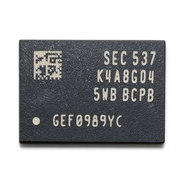
K4A8G045WB-BCPB - 8Gb DDR4 SDRAM 2Gx4 2133Mbps | Samsung
부품 번호: K4A8G045WB-BCPB ✓ 활성| 수량 | 단가 | 합계 |
|---|---|---|
| 1 | $15.4688 | $15.47 |
| 10 | $11.1719 | $111.72 |
| 100 | $9.8828 | $988.28 |
| 500 | $9.4531 | $4,726.55 |
| 1,000 | $9.0234 | $9,023.40 |
K4A8G045WB-BCPB 개요
DDR4 SDRAM (Double Data Rate 4 Synchronous Dynamic Random-Access Memory) is a volatile memory technology that transfers data on both rising and falling clock edges, doubling effective bandwidth per clock cycle. As the fourth generation of DDR memory, DDR4 succeeds DDR3 in the memory hierarchy with lower operating voltage (1.2V vs 1.5V), higher density, bank grouping, and improved on-die termination (ODT). It forms the main-memory tier in computing systems alongside cache and storage, and is the dominant DRAM generation for servers, workstations, and embedded controllers.
Key features of the K4A8G045WB-BCPB include the 2G x 4 organization for wide bus designs and ECC-enabled server DIMMs, 8n-prefetch architecture with burst length 8 (BL8) and burst chop 4 (BC4), programmable CAS latency and CAS write latency, and asynchronous reset. According to the Samsung datasheet, the device supports posted CAS, internal (self) calibration, and on-die termination via the ODT pin, with all control and address inputs synchronized to a pair of externally supplied differential clocks.
Technically, the device implements 8192 refresh cycles per 64 ms interval with auto-refresh and self-refresh modes for power conservation. The B-die design from Samsung's advanced DRAM process is known for tight timing margins and stability. DLL-enabled operation guarantees the timing specifications in the datasheet, and the 78-ball FBGA package provides excellent thermal and electrical performance with a small footprint for space-constrained memory subsystems.
Typical applications include server and workstation main memory modules, networking and communication equipment, industrial control systems, and high-performance embedded computing where 1.2V operation reduces system power versus DDR3 by roughly 20%.
When designing with this component, place decoupling capacitors close to each power pin, provide a stable 1.2V VDD and accurate VREFCA reference, and follow Samsung's fly-by routing and length-matching guidelines to preserve signal integrity at 2133 Mbps.
This page synthesizes distributor pricing, drop-in alternatives, and practical DDR4 design notes not found in the manufacturer datasheet.
드롭인 대체품: K4A8G045WB-BCPB — 동일 패키지, 핀 호환. PCB 재작업이 필요한 다른 패키지 부품은 제외됩니다.
이 시리즈의 변형
다음과 드롭인 호환되는 동일 시리즈 모델: K4A8G045WB-BCPB (동일 폼 팩터 및 풋프린트) — 차이점: Operating Temperature, Memory Type, Package, Clocking, Data Rate.
빠른 비교 도구 — 나란히 비교할 대체 부품을 선택하십시오:
K4A8G045WB-BCRC
✓ 재고 있음
$2.95 / 개
데이터시트 보기 →K4A8G085WB-BCPB
✓ 재고 있음
$13.7813 / 개
데이터시트 보기 →K4A8G085WB-BCRC
✓ 재고 있음
$6.8 / 개
데이터시트 보기 →K4A8G085WB-BCTD
✓ 재고 있음
$7.5 / 개
데이터시트 보기 →K4A8G165WB-BCPB
✓ 재고 있음
$2.3 / 개
데이터시트 보기 →K4A8G045WB-BCPB 최대 정격 & 전기적 특성
| 메모리 유형 | DDR4 SDRAM (B-die) |
| Density | 8 Gb |
| 메모리 구성 | 2G x 4 |
| 데이터 속도 | 2133 Mbps/pin (PC4-2133) |
| Supply Voltage (VDD) | 1.2 V |
| 패키지 | 78-ball FBGA |
| 실장 유형 | Surface Mount |
| Prefetch Architecture | 8n |
| Burst Length | BL8, BC4 (burst chop) |
| Refresh Cycles | 8192 |
| Refresh Modes | Auto-refresh, Self-refresh |
| Termination | On-Die Termination (ODT) |
| Reset | Asynchronous Reset |
| Clocking | Differential clocks (CK/CK#) |
| 동작 온도 | 0C to +85C |
| Max Supply Current | 211.7 mA |
| 특징 | Posted CAS, Programmable CWL, Internal (Self) Calibration |
K4A8G045WB-BCPB 78-ball fbga 핀 구성 가이드
K4A8G045WB-BCPB(78-ball fbga 패키지)의 핀 구성입니다. 이 디지털 IC에는 GPIO, 통신 인터페이스(UART, SPI, I2C), 전원 핀이 포함되어 있습니다. 대체 핀 기능과 구성 옵션은 제조사 데이터시트를 참조하십시오. 임베디드 시스템 설계와 PCB 레이아웃에 필수적입니다.

다음에 대한 상세 핀아웃 데이터 없음: K4A8G045WB-BCPB.
다음을 참조하십시오: 데이터시트 전체 핀 구성은 다음을 참조하십시오.
일반적인 애플리케이션
K4A8G045WB-BCPB 적합 용도: 6 애플리케이션s: Server ECC Main Memory, Networking and Communication Equipment, Industrial Control Systems, High-Performance Embedded Computing, Memory Module Manufacturing, Automotive Infotainment and ADAS.
Server ECC Main Memory
The K4A8G045WB-BCPB's x4 organization is the industry-standard building block for registered ECC DIMMs: a 72-bit server data bus is assembled from 18 x4 devices, reserving 8 bits for ECC correction. Its 2133 Mbps/pin data rate matches DDR4-2133 registered module platforms, and the 8192-cycle refresh plus Samsung B-die reliability supports 24/7 server uptime. At 1.2V, module power drops roughly 20% versus DDR3 RDIMMs at the same density, reducing data-center thermal load. Designers should follow JEDEC RDIMM fly-by clock routing and per-device decoupling to preserve signal integrity at full data rate.
추천
Networking and Communication Equipment
Routers, switches, and telecom line cards use DDR4 main memory for packet buffering and table lookups. The K4A8G045WB-BCPB fits these designs because its x4 organization allows wide parallel buses for high aggregate bandwidth, while 2133 Mbps/pin operation sustains line-rate throughput. The asynchronous reset pin enables deterministic power-state control during hot-swap or failover events, and self-refresh mode preserves buffer contents during low-activity periods. Differential clocking (CK/CK#) and on-die termination reduce reflections on the multi-drop point-to-point traces typical of switch fabric memory, but length matching and reference-plane continuity remain critical at this data rate.
추천
Industrial Control Systems
Industrial PCs, PLCs, and machine-vision controllers require dense, reliable DDR4 main memory tolerant of 0C to +85C ambient conditions. The K4A8G045WB-BCPB provides 8Gb per device, letting a single controller channel reach 4 GB with eight devices, and its internal (self) calibration maintains timing margins across temperature drift without host intervention. At 1.2V, DRAM contributes less heat inside sealed enclosures than DDR3 equivalents. Designers should verify conduction or fan-based cooling for the FBGA package under continuous load and ensure VREFCA reference stability in electrically noisy factory environments with proper grounding and filtering.
추천
High-Performance Embedded Computing
VPX, COM Express, and custom SoC boards embed the K4A8G045WB-BCPB as main memory next to processors requiring DDR4 interfaces. Its 8n-prefetch BL8/BC4 burst modes let memory controllers tune efficiency: BL8 maximizes sequential bandwidth for streaming workloads, while BC4 shortens bursts for random-access patterns common in real-time processing. The 78-ball FBGA footprint enables compact multi-device stacking beside the SoC. Because B-die timing is specified in DLL-enabled mode, controllers must allow DLL lock time at boot, and trace-length matching to the processor's fly-by topology must meet the 2133 Mbps eye mask across the operating temperature range.
추천
Memory Module Manufacturing
Module makers building UDIMM, RDIMM, and custom memory assemblies use the K4A8G045WB-BCPB for x4-based ECC modules at DDR4-2133. Samsung's B-die process yields consistent die-to-die timing, simplifying bin-matching across the 9 to 18 devices on a module. The 78-ball FBGA land pattern is standard across the K4A8G045WB/K4A8G085WB/K4A8G165WB families, allowing one PCB layout to serve multiple organizations and speed bins, which reduces tooling cost. Manufacturers should follow Samsung's module design guide for serialized address/command topology, per-rank termination, and thermal sensor placement to certify module reliability at full data rate.
추천
Automotive Infotainment and ADAS
Automotive head units, digital clusters, and ADAS sensor-fusion platforms use DDR4 SDRAM for map rendering, camera-frame buffering, and neural-network inference. The K4A8G045WB-BCPB's 8Gb density supports high-resolution graphics frame buffers, while x4 organization allows ECC-protected wide buses that improve functional-safety margins against single-bit errors. Its 1.2V operation eases thermal design inside dashboards, and asynchronous reset supports the rapid power-state transitions required by ignition sequencing. Note that this commercial-grade part is not AEC-Q100 qualified; automotive programs must either verify qualification status for the specific grade or select Samsung's automotive-qualified DDR4 order codes.
추천
추천 제품 요약
엔지니어링 참조 데이터: K4A8G045WB-BCPB — 비교, 설계 지침 및 규정 준수 정보.
선택 가이드
대체품과의 비교
| 파라미터 | 이 제품 | K4A8G045WB-BCRC | K4A8G085WB-BCPB | K4A8G085WB-BCRC | K4A8G165WB-BCPB |
|---|---|---|---|---|---|
| Package | 78-ball FBGA | 78-ball FBGA - same | 78-ball FBGA - same | 78-ball FBGA - same | 78-ball FBGA - same |
| Brand | Samsung Electronics | Samsung Electronics | Samsung Electronics | Samsung Electronics | Samsung Electronics |
| Density | 8 Gb | 8 Gb | 8 Gb | 8 Gb | 8 Gb |
| Organization | 2G x 4 | 2G x 4 | 1G x 8 | 1G x 8 | 512M x 16 |
| Supply Voltage | 1.2 V | 1.2 V | 1.2 V | 1.2 V | 1.2 V |
| Refresh Cycles | 8192 | 8192 | 8192 | 8192 | 8192 |
| Package Type (per distributor data) | FBGA, 78 terminals | FBGA-78 | FBGA-78 | FBGA-78 | FBGA-78 |
주요 차별점
- x4 organization optimized for ECC buses (vs K4A8G085WB-BCPB)
- B-die process with consistent timing margins (vs K4A8G045WB-BCRC)
- Reduced system power vs DDR3 (vs K4B4G1646D-BCK0 (DDR3))
설계 노트
At 2133 Mbps/pin, DDR4 timing budgets are tight. Route address/command in fly-by topology with length-matched stubs under the per-byte-lane tolerance from Samsung's design guide, and reference all high-speed traces to a continuous ground plane. Enable on-die termination (ODT) per rank and calibrate VREFDQ during initialization; incorrect ODT settings are the most common cause of marginal eye diagrams. Simulate the 2133 Mbps eye mask for the longest trace in your stack-up before releasing the PCB.
Provide three supplies: VDD/VDDQ at 1.2V, VPP at 2.5V, and VREFCA/VREFDQ references generated per the DDR4 specification. Distributor parametric data lists a maximum supply current of 211.7 mA per device; with 9-18 devices per module channel, size the VRM for aggregate peak plus margin. Place a bulk capacitor per rank and 0.1uF ceramics at each power ball group. Inrush at power-up is significant when all devices enter precharge simultaneously - verify controller power-ramp sequencing.
Timing parameters in the Samsung datasheet are specified for DLL-enabled mode only - do not operate the part DLL-off while assuming datasheet timings. The BCPB suffix is a specific speed bin; substituting a different bin (e.g., BCRC) requires reprogramming controller timing registers (CL, CWL, tRCD, tRP). Verify the 0C to +85C commercial temperature range against your product's ambient profile, and confirm -BCPB remains active (not EOL) with your distributor before committing production volumes.
규정 준수 정보
Compliance data was not included in the verified web data retrieved for this part. Consult Samsung's official environmental reports for the exact ordering code before releasing into a compliance-controlled BOM. This is a commercial-grade (0C to +85C) DRAM, not an automotive AEC-Q100 part.
