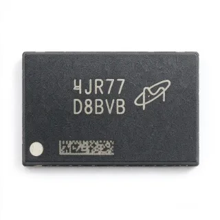
AS4C512M16D4A-62BCNTR - 8Gb DDR4 SDRAM 512Mx16 | Alliance Memory
MPN: AS4C512M16D4A-62BCNTR ✓ Active| Qty | Unit Price | Extended |
|---|---|---|
| 1 | $12.5 | $12.50 |
| 10 | $11.2 | $112.00 |
| 100 | $9.8 | $980.00 |
| 500 | $8.9 | $4,450.00 |
| 1,000 | $8.1 | $8,100.00 |
AS4C512M16D4A-62BCNTR Overview
DDR4 SDRAM (Double Data Rate 4 Synchronous Dynamic Random-Access Memory) is a type of volatile memory that transfers data on both edges of the clock signal, doubling the data rate compared to DDR3. It operates at a lower voltage (1.2V) than DDR3 (1.5V), reducing power consumption. DDR4 is the industry standard for modern computing, offering higher density and speed while maintaining backward compatibility with JEDEC standards.
Key features include a 1.2V power supply, 1600MHz clock rate (PC4-3200), 18ns CAS latency, and a 96-ball FBGA package. The device supports on-die termination (ODT), programmable read/write latencies, and auto-refresh and self-refresh modes. It is available in commercial temperature range (0°C to +95°C) and is RoHS compliant.
The AS4C512M16D4A-62BCNTR uses a 20nm-class process technology, offering high density and low power. It features a 16n prefetch architecture, which improves bandwidth efficiency. The device includes a temperature sensor for thermal management and supports DLL (Delay-Locked Loop) for precise timing.
Typical applications include servers, networking equipment, industrial PCs, and embedded systems requiring high-capacity, high-speed memory. Its 512M x 16 organization is ideal for systems with a 16-bit data bus, such as high-end routers and switches.
When designing with this device, ensure proper decoupling capacitors near the power pins and follow the layout guidelines in the datasheet to minimize signal integrity issues. The device requires a 1.2V supply and a separate VPP (2.5V) for wordline boost, which must be generated correctly.
Drop-in alternatives for AS4C512M16D4A-62BCNTR — same package, pin-to-pin compatible. Different-package parts requiring PCB rework are excluded.
Variants in this series
Same-series models that are drop-in compatible with AS4C512M16D4A-62BCNTR (same form factor and footprint) — differing in Data Rate, Package, Operating Temperature Range, Interface, Supply Voltage.
Quick Comparison Tool — Select alternative parts for side-by-side comparison:
AS4C512M16D4A-62BCN
✅ Drop-In✓ In Stock
$7.2 / Unit
View Datasheet →AS4C512M16D4A-62BIN
✅ Drop-In✓ In Stock
$8.1 / Unit
View Datasheet →AS4C512M16D4B-62BCNTR
✅ Drop-In✓ In Stock
$8.1 / Unit
View Datasheet →MT40A512M16TB-062E
✅ Drop-In ⚠️ Specs Unverified✓ In Stock
$60 / Unit
View Datasheet →K4A8G165WC-BCWE
✅ Drop-In ⚠️ Specs Unverified✓ In Stock
$38 / Unit
View Datasheet →NT5AD512M16C4-JRI
✅ Drop-In ⚠️ Specs Unverified✓ In Stock
$75.58 / Unit
View Datasheet →AS4C512M16D4A-62BCNTR Maximum Ratings & Electrical Characteristics
| Memory Type | DDR4 SDRAM |
| Memory Size | 8 Gbit (512M x 16) |
| Supply Voltage | 1.14V ~ 1.26V (nominal 1.2V) |
| Clock Rate | 1600 MHz (DDR4-3200) |
| CAS Latency | 18 ns |
| Package | 96-FBGA (7.5x13 mm) |
| Operating Temperature | 0°C to +95°C (Commercial) |
| Interface | POD (Pseudo Open Drain) |
| Data Rate | 3200 MT/s |
| Refresh | Auto-refresh and self-refresh |
| RoHS | Compliant |
| Moisture Sensitivity Level | 3 (168 Hours) |
| Write Cycle Time - Word, Page | 15 ns |
| Mounting Type | Surface Mount |
| Standard Pack | 1500/reel (Tape & Reel) |
AS4C512M16D4A-62BCNTR Pin Configuration
| Pin A1 | VDD — Power supply (1.2V) |
| Pin A2 | DQ0 — Data input/output 0 |
| Pin A3 | DQ1 — Data input/output 1 |
| Pin A4 | VSS — Ground |
| Pin A5 | DQ2 — Data input/output 2 |
| Pin A6 | DQ3 — Data input/output 3 |
| Pin A7 | VDD — Power supply (1.2V) |
| Pin A8 | DQ4 — Data input/output 4 |
| Pin A9 | DQ5 — Data input/output 5 |
| Pin A10 | VSS — Ground |
| Pin A11 | DQ6 — Data input/output 6 |
| Pin A12 | DQ7 — Data input/output 7 |
| Pin B1 | VDDQ — DQ power supply (1.2V) |
| Pin B2 | VSSQ — DQ ground |
| Pin B3 | DM0 — Data mask 0 |
| Pin B4 | DQS0_t — Data strobe 0 (true) |
| Pin B5 | DQS0_c — Data strobe 0 (complement) |
| Pin B6 | VSSQ — DQ ground |
| Pin B7 | VDDQ — DQ power supply (1.2V) |
| Pin B8 | DM1 — Data mask 1 |
| Pin B9 | DQS1_t — Data strobe 1 (true) |
| Pin B10 | DQS1_c — Data strobe 1 (complement) |
| Pin B11 | VSSQ — DQ ground |
| Pin B12 | VDDQ — DQ power supply (1.2V) |
| Pin C1 | A0 — Address input 0 |
| Pin C2 | A1 — Address input 1 |
| Pin C3 | A2 — Address input 2 |
| Pin C4 | A3 — Address input 3 |
| Pin C5 | A4 — Address input 4 |
| Pin C6 | A5 — Address input 5 |
| Pin C7 | A6 — Address input 6 |
| Pin C8 | A7 — Address input 7 |
| Pin C9 | A8 — Address input 8 |
| Pin C10 | A9 — Address input 9 |
| Pin C11 | A10/AP — Address input 10 / Auto-precharge |
| Pin C12 | A11 — Address input 11 |
| Pin D1 | A12 — Address input 12 |
| Pin D2 | A13 — Address input 13 |
| Pin D3 | A14 — Address input 14 |
| Pin D4 | A15 — Address input 15 |
| Pin D5 | BA0 — Bank address 0 |
| Pin D6 | BA1 — Bank address 1 |
| Pin D7 | BG0 — Bank group 0 |
| Pin D8 | BG1 — Bank group 1 |
| Pin D9 | CKE — Clock enable |
| Pin D10 | CS_n — Chip select (active low) |
| Pin D11 | ODT — On-die termination |
| Pin D12 | RAS_n — Row address strobe (active low) |
| Pin E1 | CAS_n — Column address strobe (active low) |
| Pin E2 | WE_n — Write enable (active low) |
| Pin E3 | ACT_n — Activate (active low) |
| Pin E4 | PAR — Parity input |
| Pin E5 | ALERT_n — Alert output (active low) |
| Pin E6 | RESET_n — Reset (active low) |
| Pin E7 | VDD — Power supply (1.2V) |
| Pin E8 | VSS — Ground |
| Pin E9 | VPP — Wordline boost supply (2.5V) |
| Pin E10 | VDD — Power supply (1.2V) |
| Pin E11 | VSS — Ground |
| Pin E12 | VDDQ — DQ power supply (1.2V) |
| Pin F1 | VSSQ — DQ ground |
| Pin F2 | DQ8 — Data input/output 8 |
| Pin F3 | DQ9 — Data input/output 9 |
| Pin F4 | VDDQ — DQ power supply (1.2V) |
| Pin F5 | DQ10 — Data input/output 10 |
| Pin F6 | DQ11 — Data input/output 11 |
| Pin F7 | VSSQ — DQ ground |
| Pin F8 | DQ12 — Data input/output 12 |
| Pin F9 | DQ13 — Data input/output 13 |
| Pin F10 | VDDQ — DQ power supply (1.2V) |
| Pin F11 | DQ14 — Data input/output 14 |
| Pin F12 | DQ15 — Data input/output 15 |
| Pin G1 | VSS — Ground |
| Pin G2 | VDD — Power supply (1.2V) |
| Pin G3 | VSS — Ground |
| Pin G4 | VDD — Power supply (1.2V) |
| Pin G5 | VSS — Ground |
| Pin G6 | VDD — Power supply (1.2V) |
| Pin G7 | VSS — Ground |
| Pin G8 | VDD — Power supply (1.2V) |
| Pin G9 | VSS — Ground |
| Pin G10 | VDD — Power supply (1.2V) |
| Pin G11 | VSS — Ground |
| Pin G12 | VDD — Power supply (1.2V) |
| Pin H1 | NC — No connect |
| Pin H2 | NC — No connect |
| Pin H3 | NC — No connect |
| Pin H4 | NC — No connect |
| Pin H5 | NC — No connect |
| Pin H6 | NC — No connect |
| Pin H7 | NC — No connect |
| Pin H8 | NC — No connect |
| Pin H9 | NC — No connect |
| Pin H10 | NC — No connect |
| Pin H11 | NC — No connect |
| Pin H12 | NC — No connect |
Typical Applications
AS4C512M16D4A-62BCNTR is suitable for 6 applications: Networking Equipment, Industrial Computing, Data Center Servers, Consumer Electronics, Automotive Infotainment, Telecommunications.
Networking Equipment
The AS4C512M16D4A-62BCNTR provides high-density, high-bandwidth memory for routers, switches, and network appliances. Its 8Gb capacity and 3200 MT/s data rate support packet buffering, routing tables, and flow processing. The 1.2V operation reduces power consumption in always-on network infrastructure. With a 96-ball FBGA package, it fits compact line cards. The commercial temperature range is suitable for indoor networking equipment. Its JEDEC compliance ensures compatibility with standard DDR4 controllers used in network processors.
Recommended
Industrial Computing
In industrial PCs and embedded systems, the AS4C512M16D4A-62BCNTR offers reliable, high-speed memory for data acquisition, control, and HMI applications. Its 8Gb density supports large application footprints and data logging. The 1.2V supply reduces heat generation, important in sealed enclosures. The 96-ball FBGA package is robust for vibration-prone environments. The commercial temperature range (0°C to +95°C) is adequate for most factory floors. JEDEC compliance ensures easy integration with standard industrial motherboards.
Recommended
Data Center Servers
The AS4C512M16D4A-62BCNTR is ideal for server main memory, providing 8Gb capacity per chip to build large-capacity DIMMs. Its 3200 MT/s data rate meets the bandwidth demands of cloud computing and virtualization. The 1.2V operation contributes to energy efficiency in data centers. The 96-ball FBGA package is standard for DDR4 RDIMMs and UDIMMs. The commercial temperature range is suitable for controlled server environments. JEDEC compliance ensures compatibility with server memory controllers.
Recommended
Consumer Electronics
In high-end consumer devices like gaming consoles, set-top boxes, and smart TVs, the AS4C512M16D4A-62BCNTR provides fast, low-power memory for smooth graphics and multitasking. Its 8Gb capacity supports large media buffers and app data. The 1.2V supply extends battery life in portable devices. The 96-ball FBGA package is compact for slim designs. The commercial temperature range covers typical consumer use. JEDEC compliance ensures compatibility with consumer SoCs.
Recommended
Automotive Infotainment
Although the commercial temperature grade limits extreme automotive use, the AS4C512M16D4A-62BCNTR can be used in infotainment systems operating in controlled cabin environments. Its 8Gb capacity supports navigation maps, media playback, and instrument cluster graphics. The 1.2V operation reduces heat in the dashboard. The 96-ball FBGA package withstands vibration. For under-hood applications, consider the industrial grade AS4C512M16D4A-62BIN. JEDEC compliance ensures compatibility with automotive SoCs.
Recommended
Telecommunications
In telecom base stations and switches, the AS4C512M16D4A-62BCNTR provides high-bandwidth memory for signal processing and protocol handling. Its 8Gb density supports large buffers for voice and data traffic. The 1.2V supply reduces power in remote radio units. The 96-ball FBGA package is suitable for compact line cards. The commercial temperature range is acceptable for indoor telecom equipment. JEDEC compliance ensures compatibility with telecom processors.
Recommended
Recommended Products Summary
Engineering reference data for AS4C512M16D4A-62BCNTR — comparison, design guidance, and compliance information.
Selection Guide
Comparison with Alternatives
| Parameter | This Product | AS4C512M16D4A-62BCN | AS4C512M16D4A-62BIN | AS4C512M16D4B-62BCNTR | MT40A512M16TB-062E | K4A8G165WC-BCWE | NT5AD512M16C4-JRI |
|---|---|---|---|---|---|---|---|
| Package | 96-FBGA (7.5x13) | 96-FBGA (7.5x13) | 96-FBGA (7.5x13) | 96-FBGA (7.5x13) | 96-FBGA (7.5x13) | 96-FBGA (7.5x13) | 96-FBGA (7.5x13) |
| Brand | Alliance Memory | Alliance Memory | Alliance Memory | Alliance Memory | Micron Technology | Samsung Electronics | NXP Semiconductors |
| Memory Size | 8 Gbit | 8 Gbit | 8 Gbit | 8 Gbit | 8 Gbit | 8 Gbit | 8 Gbit |
| Organization | 512M x 16 | 512M x 16 | 512M x 16 | 512M x 16 | 512M x 16 | 512M x 16 | 512M x 16 |
| Supply Voltage | 1.2V (1.14-1.26V) | 1.2V (1.14-1.26V) | 1.2V (1.14-1.26V) | 1.2V (1.14-1.26V) | 1.2V (1.14-1.26V) | 1.2V (1.14-1.26V) | 1.2V (1.14-1.26V) |
| Clock Rate | 1600 MHz | 1600 MHz | 1600 MHz | 1600 MHz | 1600 MHz | 1600 MHz | 1600 MHz |
Key Differentiators
- Commercial temperature grade with 0°C to +95°C range (vs AS4C512M16D4A-62BIN)
- CAS latency of 18ns (vs AS4C512M16D4B-62BCNTR)
- Tape and reel packaging for automated assembly (vs AS4C512M16D4A-62BCN)
Design Notes
The AS4C512M16D4A-62BCNTR requires a 1.2V VDD supply and a separate 2.5V VPP supply for wordline boost. Ensure these supplies are clean and well-regulated. Use 0.1uF decoupling capacitors close to each VDD and VDDQ pin, and a 10uF bulk capacitor near the power entry point. The VPP supply should be capable of sourcing transient current during write operations.
For high-speed DDR4 signals, maintain controlled impedance of 40-50 ohms for DQ, DQS, and address/command lines. Keep trace lengths matched within +/- 10 mils for data groups. Use ground planes beneath the FBGA package to minimize noise. Follow the layout guidelines in the Alliance Memory datasheet for optimal signal integrity.
The AS4C512M16D4A-62BCNTR has a maximum operating temperature of +95°C. In high-ambient environments, ensure adequate airflow or heatsinking. The 96-ball FBGA package has a thermal resistance of approximately 20°C/W (theta_JA) with proper PCB copper. Monitor junction temperature to avoid exceeding the absolute maximum rating of +95°C.
Compliance Information
RoHS compliant per distributor listings. Not AEC-Q100 qualified. Lead-free per datasheet.