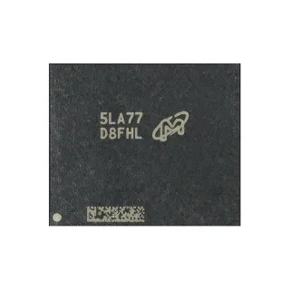
H5ANAG4NBJR-PBC - 16Gb DDR4 SDRAM | SK hynix | Main Memory
MPN: H5ANAG4NBJR-PBC ✓ Active| Qty | Unit Price | Extended |
|---|---|---|
| 1 | $0 | $0.00 |
| 10 | $0 | $0.00 |
| 100 | $0 | $0.00 |
| 500 | $0 | $0.00 |
| 1,000 | $0 | $0.00 |
H5ANAG4NBJR-PBC Overview
DDR4 SDRAM is the fourth generation of double-data-rate synchronous dynamic random-access memory, the dominant main-memory technology in servers, workstations, desktops, and embedded systems. Compared with DDR3, DDR4 provides higher transfer rates, lower operating voltage (1.2V VDD versus 1.5V), bank-group architecture for faster random access, and improved on-die termination (ODT) schemes. In the system hierarchy it sits as the main system memory tier between CPU caches and storage.
Key features of the H5ANAG4NBJR family include high 16Gb (2G x4 / 1G x8 / 512M x16 organization class) density per die, the DDR4 bank-group architecture that shortens random row/column access cycling, programmable CAS latency and additive latency, on-die termination, and CRC/write parity features for data integrity in reliability-sensitive designs.
Architecturally, the die is a CMOS DRAM organized into banks and bank groups, supporting burst lengths of 8 (BL8) with DDR4 burst-chop options, and supports the standard DDR4 mode-register set (MR0-MR6) for configuration. The device is specified by SK hynix as ideally suited for main memory applications requiring large memory density and high bandwidth, per the family datasheet.
Typical applications include server DIMM modules and memory down designs, industrial PCs, networking equipment line cards, and embedded computing platforms. When paired with a DDR4 memory controller that supports bank-group timing (tCCD_S/tCCD_L), the device sustains high sustained bandwidth.
Design consideration: DDR4 requires careful attention to signal integrity - fly-by addressing topology, per-byte termination, and VDDQ decoupling. Follow JEDEC DDR4 layout guidance and the SK hynix datasheet recommendations for ball map and reference design.
This page synthesizes distributor data, same-family drop-in alternatives, and practical design notes beyond the raw datasheet to support sourcing and design decisions.
Drop-in alternatives for H5ANAG4NBJR-PBC — same package, pin-to-pin compatible. Different-package parts requiring PCB rework are excluded.
Variants in this series
Same-series models that are drop-in compatible with H5ANAG4NBJR-PBC (same form factor and footprint) — differing in RoHS Status, Package, Interface, Density, Organization.
Quick Comparison Tool — Select alternative parts for side-by-side comparison:
H5ANAG6NBJR-PBC
✅ Drop-In✓ In Stock
$6.45 / Unit
View Datasheet →H5ANAG8NBJR-PBC
✅ Drop-In✓ In Stock
$31.5 / Unit
View Datasheet →H5ANAG6NBJR-VKC
✅ Drop-In✓ In Stock
$15 / Unit
View Datasheet →H5ANAG6NBJR-UHC
✅ Drop-In✓ In Stock
$8.09 / Unit
View Datasheet →H5ANAG6NBJR-RDC
✅ Drop-In✓ In Stock
$9.6 / Unit
View Datasheet →H5ANAG8NBJR-VKC
✅ Drop-In✓ In Stock
$8.6 / Unit
View Datasheet →H5ANAG8NBJR-RDC
✅ Drop-In✓ In Stock
$3.55 / Unit
View Datasheet →H5ANAG4NBJR-PBC Maximum Ratings & Electrical Characteristics
| Manufacturer | SK hynix |
| Product Family | H5ANAG4NBJR-xxC 16Gb DDR4 SDRAM |
| Memory Type | DDR4 SDRAM |
| Density | 16 Gbit |
| Package Code | TFBGA |
| Package Shape | Rectangular |
| Number of Terminals | 96 |
| Interface | DDR4 parallel interface |
| Speed Grade Suffix | PBC (per SK hynix part number decoder) |
| Temperature Grade | OTHER (per Partstack listing for H5AN4G6NBJR-PBC family) |
| Lead Free | Yes (PBC suffix, per SK hynix part number decoder) |
| Halogen Free | Yes (PBC suffix, per SK hynix part number decoder) |
| RoHS Status | Compliant (family datasheet: Lead-Free & Halogen-Free, RoHS Compliant) |
| Mounting Type | Surface Mount |
| Configuration Support | x4 / x8 / x16 per family organization options |
H5ANAG4NBJR-PBC rectangular Pin Configuration Guide
Pin configuration for H5ANAG4NBJR-PBC (rectangular package). This digital IC includes GPIO, communication interfaces (UART, SPI, I2C), and power pins. Refer to the manufacturer datasheet for alternate pin functions and configuration options. Essential for embedded system design and PCB layout.

No detailed pinout data available for H5ANAG4NBJR-PBC.
Refer to the datasheet for full pin configuration.
Typical Applications
H5ANAG4NBJR-PBC is suitable for 6 applications: Server Main Memory (RDIMM/LRDIMM), Industrial PC and Embedded Computing, Networking Equipment Line Cards, Test and Measurement Instruments, Video Surveillance and Display Systems, Automotive-Adjacent and Rugged Edge Systems.
Server Main Memory (RDIMM/LRDIMM)
The H5ANAG4NBJR-PBC's 16Gb DDR4 SDRAM density is a core building block for server RDIMM and LRDIMM modules, where maximum capacity per rank and ECC support dominate the design. SK hynix specifies the DDR4 family as ideally suited for main memory applications requiring large memory density and high bandwidth. In x4-organization server modules, x4 devices enable chipkill-class error correction, critical for data-center reliability targets. The DDR4 bank-group architecture shortens random column-to-column cycling (separate tCCD_S/tCCD_L), sustaining high effective bandwidth under virtualized workloads. Designers should follow the module's fly-by address topology and per-device termination per JEDEC DDR4 module specifications, and program SPD data so the server BIOS trains correct timing for the PBC speed bin.
Recommended
Industrial PC and Embedded Computing
Industrial PCs, edge controllers, and embedded x86/ARM platforms use memory-down DDR4 designs where the H5ANAG4NBJR-PBC provides high 16Gb density on the CPU board without a module connector, improving vibration tolerance and reducing height. SK hynix consumer/industrial DDR4 documentation specifies case-temperature support requirements, and designers must verify the specific PBC bin's operating range from the official datasheet. The DDR4 interface integrates directly with embedded DDR4 controllers (Intel Atom, AMD Ryzen Embedded), with on-die termination simplifying point-to-point routing. The RoHS-compliant, lead-free, halogen-free construction supports industrial environmental compliance. Memory-down designs should follow controller reference designs for length matching and use the controller's DDR4 training firmware for the PBC timing bin.
Recommended
Networking Equipment Line Cards
Switch, router, and network-appliance line cards use the H5ANAG4NBJR-PBC as deep-packet-buffer and control-plane memory, where 16Gb per device allows large flow tables and burst absorption without external queue management. DDR4's high bandwidth matches the demands of multi-core network processors and SmartNIC SoCs, and the bank-group architecture improves random access performance typical of packet lookups. The 96-ball TFBGA footprint supports compact memory-down layouts on dense line cards. Designers should place the DRAM close to the network processor, follow per-byte-lane length matching, and provision adequate VDDQ decoupling because packet-processing workloads cause fast bursty current transitions that stress the power delivery network.
Recommended
Test and Measurement Instruments
Oscilloscopes, logic analyzers, and signal generators require large acquisition memory with sustained write bandwidth; the H5ANAG4NBJR-PBC's 16Gb DDR4 density and DDR4 bandwidth serve as deep sample memory behind high-speed acquisition front ends. SK hynix's DDR4 architecture supports burst writing from ADC streaming pipelines, and the PBC speed bin should be selected to match the acquisition controller's supported data rate. Memory-down TFBGA placement near the acquisition FPGA minimizes trace length and crosstalk. Instrument designers should implement controller-based periodic refresh scheduling and verify the datasheet's case-temperature limits for the expected internal-instrument environment, since sustained streaming keeps utilization - and self-heating - high.
Recommended
Video Surveillance and Display Systems
Network video recorders, smart-camera SoCs, and display-processing platforms use the H5ANAG4NBJR-PBC as frame-buffer and analytics memory, where 16Gb per device holds multiple high-resolution video streams plus AI inference buffers. DDR4 bandwidth sustains simultaneous 4K encode/decode pipelines typical of modern surveillance SoCs, and on-die termination simplifies the memory-down layout common in camera housings with strict height constraints. The RoHS-compliant, lead-free, halogen-free construction supports global deployment of surveillance hardware. Designers should size the frame-buffer ring so that the DDR4 bus utilization stays below roughly 70 percent to preserve headroom for burst refresh and bus-turnaround penalties under multi-stream workloads.
Recommended
Automotive-Adjacent and Rugged Edge Systems
Rugged edge gateways, telematics hubs, and driver-assistance prototyping platforms deploy the H5ANAG4NBJR-PBC in memory-down configurations where the 96-ball TFBGA's soldered mounting improves vibration endurance versus socketed SODIMMs. SK hynix's consumer DDR4 documentation defines industrial case-temperature support windows (-40 to 85C with extended-range options in related NBJR documents), but designers must confirm the exact PBC bin rating from the official datasheet and, for true automotive deployment, select SK hynix automotive-qualified DDR4 variants instead. DDR4 training should be re-run across the full temperature range to validate guard-band timing, and thermal design should keep case temperature within the datasheet limit under worst-case sustained memory traffic.
Recommended
Recommended Products Summary
Engineering reference data for H5ANAG4NBJR-PBC — comparison, design guidance, and compliance information.
Selection Guide
Comparison with Alternatives
| Parameter | This Product | H5ANAG6NBJR-PBC | H5ANAG8NBJR-PBC | H5ANAG6NBJR-VKC | H5ANAG6NBJR-UHC | H5ANAG8NBJR-RDC |
|---|---|---|---|---|---|---|
| Package | TFBGA-96 (rectangular) | TFBGA-96 - same | TFBGA-96 - same | TFBGA-96 - same | TFBGA-96 - same | TFBGA-96 - same |
| Brand | SK hynix | SK hynix | SK hynix | SK hynix | SK hynix | SK hynix |
| Memory Type | DDR4 SDRAM | DDR4 SDRAM | DDR4 SDRAM | DDR4 SDRAM | DDR4 SDRAM | DDR4 SDRAM |
| Die Organization Code | AG4 | AG6 | AG8 | AG6 | AG6 | AG8 |
| Speed/Temperature Suffix | PBC | PBC - same | PBC - same | VKC | UHC | RDC |
| Number of Terminals | 96 | 96 | 96 | 96 | 96 | 96 |
| Controller Organization Compatibility | x4-class server/ECC designs (per AG4 code) | AG6 organization - x8-class module designs | AG8 organization - wide-bus designs | AG6 organization, VKC timing bin | AG6 organization, UHC timing bin | AG8 organization, RDC timing bin |
Key Differentiators
- x4-class organization for ECC-rich server designs (vs H5ANAG6NBJR-PBC)
- Identical PBC speed bin available across organizations (vs H5ANAG8NBJR-PBC)
- Higher timing bin than RDC-graded family members (vs H5ANAG8NBJR-RDC)
Design Notes
DDR4 SDRAM interfaces are extremely timing-sensitive. Route address/command in a fly-by or point-to-point topology per the memory controller reference design, length-match data lanes within each byte lane to tighter than controller skew budget, and reference all signals to a continuous ground plane. Configure on-die termination (ODT) in accordance with the controller's training algorithm - incorrect ODT values are the most common cause of marginal DDR4 eye diagrams. Follow the SK hynix datasheet ball map for the 96-ball TFBGA exactly; do not re-map balls between family members, even though they share the footprint.
DDR4 operates from separate VDD, VDDQ, and VPP rails. Provide independent decoupling at each rail: multiple 0.1uF ceramics at the ball side plus bulk capacitance sized to the controller's power-delivery recommendation. Estimated: peak burst currents on a 64-bit DDR4 bus can approach several amps of transient demand; rail ripple above the controller's specified window triggers bit errors during training. Use a dedicated VRM with remote sensing for VDDQ and sequence VPP per the JEDEC DDR4 power-up procedure implemented by the controller.
Do not assume interchangeability across the SK hynix DDR4 part number fields: the AGx die-organization code and the trailing speed/temperature suffix (PBC, VKC, UHC, RDC) each change a parameter that the memory controller and SPD data depend on. Always decode the full MPN with the SK hynix part number decoder and verify timing (CL, tRCD, tRP, data rate) and organization against the controller's supported list before a BOM swap. Also confirm the exact operating temperature of the specific bin from the official datasheet rather than inheriting values from the 4Gb H5AN4GxNBJR consumer documents.
Compliance Information
Family datasheet states Lead-Free & Halogen-Free (RoHS Compliant) for the DDR4 SDRAM series. PBC suffix per SK hynix part number decoder indicates Pb-free/halogen-free construction. REACH and conflict-minerals status not stated in provided data.