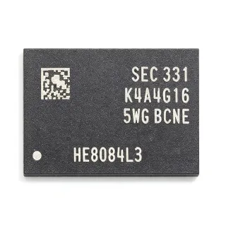
H5ANAG6NCMR-XNI - DDR4 16Gb 3200Mbps DRAM | SK Hynix
MPN: H5ANAG6NCMR-XNI ✓ Active| Qty | Unit Price | Extended |
|---|---|---|
| 1 | $6.9 | $6.90 |
| 10 | $6.4 | $64.00 |
| 100 | $5.85 | $585.00 |
| 500 | $5.4 | $2,700.00 |
| 1,000 | $4.95 | $4,950.00 |
H5ANAG6NCMR-XNI Overview
DDR4 SDRAM is the fourth generation of double-data-rate synchronous dynamic random access memory. Within the memory hierarchy, DRAM sits above NAND flash as the primary volatile working memory of a system: the memory controller issues row and column commands over a parallel interface, and the device stores each bit as charge on a capacitor that must be periodically refreshed. DDR4 improved on DDR3 by lowering the operating voltage from 1.5 V to 1.2 V, raising data rates up to 3200 Mbps and beyond, and introducing bank groups that allow faster interleaved access.
Key features of the H5ANAG6NCMR-XNI include its 16 Gbit density in a single x16 component, the -XN speed grade supporting DDR4-3200 operation, and Normal Power configuration. The x16 organization simplifies interface design for systems that use a 16-bit or 32-bit memory bus, reducing chip count compared with x8 parts at equal bus width.
Architecturally, the device implements DDR4 bank-group operation, on-die termination, and standard DDR4 command timing as defined in the SK Hynix 16Gb DDR4 family datasheet. The 1.2 V core supply, together with VPP for word-line boosting, keeps power consumption low enough for dense memory subsystems while sustaining the 3200 Mbps transfer rate of the XN bin.
Typical applications include industrial controllers, computing modules, embedded logging systems, firmware boot platforms, consumer electronics, and replacement sourcing for main-memory designs. Its high density suits systems needing 2 GB or more of DRAM from a small number of components.
Designers should verify controller support for the DDR4-3200 timing tables, implement proper fly-by routing with VTT termination, and confirm the x16 data mask and DQS pair assignments against the FBGA-96 ball map in the manufacturer datasheet.
This page synthesizes distributor inventory data, drop-in same-family alternatives, and practical DDR4 design notes not found in a single manufacturer datasheet.
Drop-in alternatives for H5ANAG6NCMR-XNI — same package, pin-to-pin compatible. Different-package parts requiring PCB rework are excluded.
Variants in this series
Same-series models that are drop-in compatible with H5ANAG6NCMR-XNI (same form factor and footprint) — differing in Package, Memory Type, Mounting Type, Interface, Memory Size.
Quick Comparison Tool — Select alternative parts for side-by-side comparison:
H5ANAG6NCMR-XNC
✅ Drop-In✓ In Stock
$31.4 / Unit
View Datasheet →H5ANAG6NCJR-XN
✅ Drop-In✓ In Stock
$71.2 / Unit
View Datasheet →H5ANAG6NCJR-XNC
✅ Drop-In✓ In Stock
$84.97 / Unit
View Datasheet →H5ANAG6NCR-XNC
✅ Drop-In✓ In Stock
$68.18 / Unit
View Datasheet →H5ANAG6NCR-VKC
✅ Drop-In✓ In Stock
Contact for price
View Datasheet →H5ANAG6NAMR-UHC
✅ Drop-In✓ In Stock
$4.5 / Unit
View Datasheet →H5ANAG6NCMR-XNI Maximum Ratings & Electrical Characteristics
| Memory Type | DDR4 SDRAM (volatile DRAM) |
| Memory Size | 16 Gb |
| Memory Organization | 1G x 16 |
| Data Rate | 3200 Mbps (DDR4-3200, XN speed bin) |
| Supply Voltage | 1.2 V |
| Technology | CMOS Double Data Rate IV Synchronous DRAM |
| Power Class | Normal Power |
| Package | FBGA-96 |
| Mounting Type | Surface Mount |
| Interface | Parallel (DDR4) |
| Product Status | Active |
| Application Domain | Main memory, industrial controllers, computing modules, consumer electronics |
| Memory Format | DRAM |
| Speed Bin Family | UH/VK/WM/XN |
H5ANAG6NCMR-XNI fbga-96 Pin Configuration Guide
Pin configuration for H5ANAG6NCMR-XNI (fbga-96 package). This digital IC includes GPIO, communication interfaces (UART, SPI, I2C), and power pins. Refer to the manufacturer datasheet for alternate pin functions and configuration options. Essential for embedded system design and PCB layout.

No detailed pinout data available for H5ANAG6NCMR-XNI.
Refer to the datasheet for full pin configuration.
Typical Applications
H5ANAG6NCMR-XNI is suitable for 6 applications: Industrial Controllers, Computing Modules and SOMs, Embedded Logging and Data Acquisition, Consumer Electronics, Firmware Boot and Networking Platforms, Replacement Sourcing and EOL Recovery.
Industrial Controllers
The H5ANAG6NCMR-XNI fits industrial controller main memory because its 16Gb x16 density provides 2 GB per component, reducing chip count on crowded control PCBs, while the 1.2 V Normal Power configuration limits heat inside sealed cabinets. At DDR4-3200 the XN speed bin supplies 3.2 GB/s per chip over a 16-bit bus, enough headroom for real-time motion control, protocol stacks, and logging buffers. Placed on a fly-by-routed DDR4 bus with on-die termination, the device trades a slightly higher cost than DDR3 for double the bandwidth and lower operating power. Verify the industrial temperature range in the SK Hynix ordering data before deployment.
Recommended
Computing Modules and SOMs
System-on-module designers use the H5ANAG6NCMR-XNI as main memory because one 16Gb component replaces two 8Gb chips at equal bus width, saving layout area on 60 x 60 mm modules. The 1Gx16 organization matches 16-bit and 32-bit controller buses without external data-width aggregation, and the DDR4-3200 XN bin delivers up to 6.4 GB/s on a 32-bit interface. Modules using fly-by routing with two components reach 4 GB capacity. The trade-off versus LPDDR4 is higher idle power from the 1.2 V DDR4 interface, which is acceptable in wall-powered edge-computing gateways and industrial PCs.
Recommended
Embedded Logging and Data Acquisition
For embedded loggers and data-acquisition systems, the H5ANAG6NCMR-XNI provides a 2 GB volatile buffer that absorbs burst data from high-rate sensors before streaming to NAND or SSD storage. The 3200 Mbps data rate sustains multi-hundred-MB/s write bursts, and the x16 data mask (DM) per byte lane enables efficient partial-word writes. Designers typically pair the DRAM with an FPGA memory controller using the DDR4-3200 timing table; refresh and self-refresh modes allow the buffer to retain contents during low-power states. Total buffer cost drops versus 8Gb parts because chip count halves for the same capacity.
Recommended
Consumer Electronics
Smart TVs, set-top boxes, and networking appliances use the H5ANAG6NCMR-XNI where 1-2 GB of DDR4 main memory is required at commodity cost. The 16Gb density covers the memory map of mid-range SoCs in one or two components, and the 1.2 V supply aligns with standard DDR4 power trees already present in consumer designs. Its 3200 Mbps capability allows SoC graphics and video decode engines to operate without bandwidth starvation at 4K frame buffers. Consumer designs should qualify the standard commercial temperature version and confirm availability of the XN bin, falling back to VKC/UHC bins if 2666-class performance is sufficient.
Recommended
Firmware Boot and Networking Platforms
Networking platforms - routers, switches, and security appliances - deploy the H5ANAG6NCMR-XNI as packet-buffer and runtime memory. A 16-bit bus at DDR4-3200 yields 3.2 GB/s per component, and multiple components on a 64-bit fly-by bus reach 12.8 GB/s, enough to sustain line-rate packet processing in gigabit-class equipment. The device's bank-group architecture improves random-access efficiency for queue-based workloads, and standard DDR4 training ensures interoperability with merchant silicon memory controllers. Pair with SPI NOR flash for firmware boot; both are stocked by the same distribution channel for BOM consolidation.
Recommended
Replacement Sourcing and EOL Recovery
The GlobalSpec product overview explicitly lists replacement sourcing as a use case for the H5ANAG6NCMR-XNI. When an original DDR4 BOM line becomes unavailable, designers can substitute same-footprint SK Hynix family members such as H5ANAG6NCMR-XNC or H5ANAG6NCJR-XN, which share the FBGA-96 land pattern and 1Gx16 organization. Procurement teams should confirm the speed-bin timing coverage of the substitute against the controller configuration and run one boot/memory-test cycle before mass swap. Keeping multiple qualified speed bins on the AVL protects against commodity DRAM allocation cycles.
Recommended
Recommended Products Summary
Engineering reference data for H5ANAG6NCMR-XNI — comparison, design guidance, and compliance information.
Selection Guide
Comparison with Alternatives
| Parameter | This Product | H5ANAG6NCMR-XNC | H5ANAG6NCJR-XN | H5ANAG6NCR-XNC | H5ANAG6NAMR-UHC |
|---|---|---|---|---|---|
| Package | FBGA-96 | FBGA-96 - same | FBGA-96 - same | FBGA-96 - same | FBGA-96 - same |
| Brand | SK Hynix | SK Hynix | SK Hynix | SK Hynix | SK Hynix |
| Memory Size | 16 Gb | 16 Gb | 16 Gb | 16 Gb | 16 Gb |
| Organization | 1G x 16 | 1G x 16 | 1G x 16 | 1G x 16 | 1G x 16 |
| Speed Bin / Data Rate | XN (DDR4-3200) | XNC | XN (DDR4-3200) | XNC | UHC (DDR4-2666 class) |
| Supply Voltage | 1.2 V | 1.2 V | 1.2 V | 1.2 V | 1.2 V |
| Power Class | Normal Power | Normal Power | Normal Power | Normal Power | Normal Power |
| Lifecycle Status | Active | Active | Active | Active | Active |
Key Differentiators
- Highest qualified data rate in the family (vs H5ANAG6NAMR-UHC)
- 16Gb x16 density halves chip count (vs H5AN8G8NCJR-XNC)
- Mainstream supply base with stock (vs H5ANAG6NCR-VKC)
Design Notes
At DDR4-3200 the H5ANAG6NCMR-XNI requires fly-by routing of address/command signals from the controller toward the last DRAM, with 40 ohm on-die termination (ODT) settings tuned during memory training. Keep DQ/DQS trace length skew within the controller specification (typically a few tens of picoseconds per byte lane) and route DQS pairs as tightly coupled differential pairs. Simulate any trace longer than approximately 100 mm for eye-mask compliance at 1600 MHz. Recommended reading: JEDEC DDR4 signal-integrity guidance and SK Hynix DDR4 design guides.
The device runs from a 1.2 V core (VDD/VDDQ) plus a VPP rail; estimate peak supply current from the DDR4-3200 timing table for your specific access pattern rather than assuming datasheet typicals. Decouple each FBGA-96 component with a network of bulk (22-47 uF) and high-frequency (0.1 uF, 0.01 uF) ceramics placed within a few millimeters of the ball field. Estimated: a 32-bit bus with two chips at high utilization can draw several hundred milliamps per rail transiently, so use a dedicated buck regulator per rail with remote sensing if the VRM is more than 50 mm away.
Do not assume all XNI/XNC speed bins have identical AC timing: the suffix defines the qualified data rate and CL/tRCD/tRP table, and controllers configured for DDR4-3200 will fail training if the substitute bin only guarantees DDR4-2666. Also verify x16-specific pins (two DM, two DQS pairs) are connected per the datasheet ball map, since x8 and x16 variants share the family name prefix but differ in ball assignment. Finally, DDR4 BGA assemblies are moisture sensitive - follow the MSL floor-life and baking requirements printed on the shipping tray label.
Compliance Information
Compliance data was not present in the verified web data for this MPN. RoHS/REACH status should be requested from SK Hynix or the distributor with the order. SK Hynix offers AEC-Q100-marketed variants in this family (AMR prefix, e.g. H5ANAG6NAMR-UHC) - the XNI commercial part is not marketed as automotive-qualified.