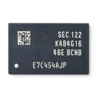
H5ANAG6NCR-VKC - 16Gb DDR4 SDRAM x8 | SK hynix | Main Memory
MPN: H5ANAG6NCR-VKC ✓ Active| Qty | Unit Price | Extended |
|---|---|---|
| 1 | $0 | $0.00 |
| 10 | $0 | $0.00 |
| 100 | $0 | $0.00 |
| 500 | $0 | $0.00 |
| 1,000 | $0 | $0.00 |
H5ANAG6NCR-VKC Overview
DDR4 SDRAM is the fourth generation of Double Data Rate synchronous DRAM, a category of volatile main-memory ICs that store data dynamically in capacitor-based cells and must be periodically refreshed. Within the memory hierarchy it sits between CPU caches and storage devices, providing the primary working memory bandwidth for processors in servers, workstations, and embedded systems. The DDR4 generation introduced bank groups, lower operating voltage, and higher data rates than DDR3.
Key features of this 16Gb monolithic die include fully synchronous operation referenced to both rising and falling edges of the clock, 8 internal banks organized into bank groups for improved effective bandwidth, and on-die termination plus DLL for signal integrity at high data rates. The VKC speed bin designation corresponds to a JEDEC-standard DDR4 data-rate grade, and the C temperature suffix indicates the commercial operating range per SK hynix part-numbering convention.
Architecturally, the device multiplexes row and column addresses on shared address pins, uses burst lengths of 8 (BL8) with programmable CAS latency, and supports DDR4 features such as activate-to-activate timing management, refresh modes (1x/2x/4X), and CRC/CA parity options depending on configuration. Power consumption benefits from the 1.2V VDD/VDDQ rails versus the 1.5V of DDR3, reducing system-level power per transferred bit.
Typical applications include server and workstation main memory modules (UDIMM, RDIMM, SODIMM), embedded computing boards, industrial PCs, networking equipment, and graphics or acceleration cards where large memory density and high bandwidth are required.
When designing with this component, follow JEDEC DDR4 routing guidelines for fly-by address/command topology, length-matched data lanes, and reference-plane integrity; power-rail decoupling on both VDD and VDDQ domains is critical for eye-mask compliance at maximum data rate.
This page synthesizes distributor availability data, same-brand drop-in speed-grade variants, and practical design notes in one reference, providing information gain beyond the raw manufacturer datasheet.
Drop-in alternatives for H5ANAG6NCR-VKC — same package, pin-to-pin compatible. Different-package parts requiring PCB rework are excluded.
Variants in this series
Same-series models that are drop-in compatible with H5ANAG6NCR-VKC (same form factor and footprint) — differing in Package, Interface, Data Rate, Memory Type, Mounting Type.
Quick Comparison Tool — Select alternative parts for side-by-side comparison:
H5ANAG6NCJR-XNC
✅ Drop-In ⚠️ Specs Unverified✓ In Stock
$84.97 / Unit
View Datasheet →H5ANAG6NCR-UHC
✅ Drop-In ⚠️ Specs Unverified✓ In Stock
$9.2 / Unit
View Datasheet →H5ANAG6NCR-RDC
✅ Drop-In ⚠️ Specs Unverified✓ In Stock
$72.1 / Unit
View Datasheet →H5ANAG6NCR-PBC
✅ Drop-In ⚠️ Specs Unverified✓ In Stock
$70.2 / Unit
View Datasheet →H5ANAG6NCJR-VKC
✅ Drop-In📋 Reference alternative (not in catalog)
H5ANAG6NAMR-UHC
✅ Drop-In ⚠️ Specs Unverified✓ In Stock
$4.5 / Unit
View Datasheet →H5ANAG6NCR-VKC Maximum Ratings & Electrical Characteristics
| Memory Type | DDR4 SDRAM |
| Memory Density | 16 Gbit |
| Organization | 2G x 8 |
| Interface | DDR4 (Double Data Rate 4) |
| Supply Voltage VDD | 1.2 V |
| Supply Voltage VDDQ | 1.2 V |
| Package | 96-ball FBGA |
| Mounting Type | Surface Mount |
| Banks | 16 banks (4 bank groups x 4) |
| Burst Length | BL8 |
| Refresh Mode | 1x / 2x / 4X per JEDEC DDR4 |
| Technology | CMOS |
| Application | Main memory (PC / server / embedded) |
H5ANAG6NCR-VKC 96-ball fbga Pin Configuration Guide
Pin configuration for H5ANAG6NCR-VKC (96-ball fbga package). This digital IC includes GPIO, communication interfaces (UART, SPI, I2C), and power pins. Refer to the manufacturer datasheet for alternate pin functions and configuration options. Essential for embedded system design and PCB layout.

No detailed pinout data available for H5ANAG6NCR-VKC.
Refer to the datasheet for full pin configuration.
Typical Applications
H5ANAG6NCR-VKC is suitable for 6 applications: Server Main Memory, Workstation and Desktop UDIMM, Embedded Computing Boards, Networking and Telecommunication Equipment, Graphics and Accelerator Cards, Test and Measurement Instrumentation.
Server Main Memory
In server platforms, the H5ANAG6NCR-VKC populates RDIMM and LRDIMM modules where its 16Gb density enables high-capacity per-DIMM configurations, for example 64GB modules built from eight x8 dies per rank. The 2G x 8 organization maps efficiently onto JEDEC DDR4 rank architectures, and the 2666-class VKC bin matches common server controller frequencies. Bandwidth scales with channel population, and bank-group architecture sustains effective throughput under the random-access patterns typical of virtualized workloads. At 1.2V VDD, power per bit is reduced versus DDR3, an important factor in datacenter TCO where memory can account for a large share of server energy consumption.
Recommended
Workstation and Desktop UDIMM
High-end desktop and workstation motherboards use 16Gb DDR4 x8 components like the H5ANAG6NCR-VKC in unbuffered DIMMs, allowing 16GB single-rank modules and 32GB dual-rank modules without doubling chip count. The 2666 Mbps class bin supports mainstream Intel and AMD DDR4-2666 memory controller speeds, and JEDEC-standard timings ensure plug-and-play compatibility at default SPD profiles. Fully synchronous operation referenced to both clock edges sustains burst throughput for content-creation workloads. Thermal requirements are modest at UDIMM power levels, relying on module airflow rather than heatsinks in most desktop chassis designs.
Recommended
Embedded Computing Boards
Industrial embedded platforms such as COM Express, ATX industrial motherboards, and network-appliance boards use the H5ANAG6NCR-VKC soldered directly on-board (down on-board memory) to save height and improve vibration tolerance versus SODIMMs. The 96-ball FBGA package supports standard reflow assembly, and the 1.2V rails integrate cleanly with modern SoC power trees. Designers must follow JEDEC DDR4 fly-by routing with length matching and on-die termination enabled to achieve the 2666-class data rate on 4-to-8 layer PCBs. The 16Gb density allows 4GB to 8GB on-board footprints with only two to four components.
Recommended
Networking and Telecommunication Equipment
Routers, switches, and 5G baseband cards require large packet buffers and flow tables, making 16Gb DDR4 x8 components a standard choice. The H5ANAG6NCR-VKC's bank-group architecture provides the effective bandwidth needed to sustain line-rate packet processing when paired with network-processing ASICs or FPGA soft memory controllers. The VKC 2666-class bin matches common fabric clock domains, and 2x/4X refresh modes allow tuning of availability versus bandwidth. On-board soldered FBGA mounting withstands the thermal cycling and vibration profiles typical of telecom central-office and outdoor equipment enclosures.
Recommended
Graphics and Accelerator Cards
Entry-level GPU boards, AI inference accelerators, and video-capture cards use DDR4 x8 components as frame-buffer and working memory where GDDR bandwidth is not required. The H5ANAG6NCR-VKC provides 16Gb per die, so four x8 devices yield 8GB on a 32-bit bus. The BL8 burst and double-data-rate clocking deliver sustained streaming bandwidth for frame storage, while 1.2V operation keeps card power budgets compliant. Signal integrity at the 2666-class rate requires careful fly-by address routing and reference-plane continuity on the accelerator PCB per JEDEC DDR4 layout practice.
Recommended
Test and Measurement Instrumentation
Oscilloscopes, logic analyzers, and protocol analyzers capture massive data streams into DDR4 memory, where the H5ANAG6NCR-VKC's 16Gb density directly extends record length. Its x8 organization with DM data masking lets instruments gate irrelevant bytes during high-speed capture, and the 2666 Mbps class rate supports deep-memory acquisitions on multi-channel scopes. Controllers pair the DRAM with FPGA memory controllers (such as Arria 10 hard memory controllers), using JEDEC training for reliable link establishment. Consistent die availability matters here, making the multiple SK hynix speed-bin drop-ins on this page valuable for long product lifecycles.
Recommended
Recommended Products Summary
Engineering reference data for H5ANAG6NCR-VKC — comparison, design guidance, and compliance information.
Selection Guide
Comparison with Alternatives
| Parameter | This Product | H5ANAG6NCJR-XNC | H5ANAG6NCR-UHC | H5ANAG6NCR-RDC | H5ANAG6NCJR-VKC |
|---|---|---|---|---|---|
| Brand | SK Hynix | SK Hynix | SK Hynix | SK Hynix | SK Hynix |
| Package | 96-ball FBGA | 96-ball FBGA - same | 96-ball FBGA - same | 96-ball FBGA - same | 96-ball FBGA - same |
| Density | 16 Gbit | 16 Gbit | 16 Gbit | 16 Gbit | 16 Gbit |
| Organization | 2G x 8 | 2G x 8 | 2G x 8 | 2G x 8 | 2G x 8 |
| Speed Grade | VKC (2666 Mbps class) | XNC (3200 Mbps class) | UHC (2400 Mbps class) | RDC (2133 Mbps class) | VKC (2666 Mbps class) |
| Interface | DDR4, 1.2 V | DDR4, 1.2 V | DDR4, 1.2 V | DDR4, 1.2 V | DDR4, 1.2 V |
| Bank Architecture | 16 banks / 4 bank groups | 16 banks / 4 bank groups | 16 banks / 4 bank groups | 16 banks / 4 bank groups | 16 banks / 4 bank groups |
| Typical Use | DDR4-2666 main memory | DDR4-3200 high-bandwidth | DDR4-2400 cost-optimized | DDR4-2133 embedded | DDR4-2666 main memory |
Key Differentiators
- Faster bin than cost-optimized variants (vs H5ANAG6NCR-UHC)
- Lower power per bit than DDR3 (vs H5AN8G6NAFR-VKC)
- Density halves chip count vs 8Gb (vs H5AN8G8NCJR-VKC)
Design Notes
Route DDR4 address/command lines in fly-by topology with on-die termination enabled, and length-match DQ/DQS strobe pairs within the JEDEC DDR4 spec window for the 2666 Mbps class. Reference all layers to solid planes, avoid stubs on DQS lines, and series-terminate address/command at the controller. Simulate the eye diagram at the target data rate before fab; VDDQ droop below spec during simultaneous switching is a leading cause of training failure on 16Gb x8 designs.
Provide separate, well-decoupled 1.2V VDD and VDDQ rails. DRAM instantaneous current spikes with burst activity, so use bulk capacitance (e.g., 100uF per rank group) plus dense 0.1uF ceramics at each VDD/VDDQ ball pair. Estimated: IDD depends on the operating profile, so use SK hynix IDD tables for the VKC bin at your frequency rather than a generic figure, and size the PMIC with margin for refresh (1x to 4X modes change current draw).
Do not mix speed bins in the same rank without validating controller training at the slowest bin's timings. Verify the exact speed bin meaning of the VKC suffix against the die-revision datasheet (NCR vs JR revisions exist in this family), since suffix conventions can shift between die generations. Confirm the C temperature suffix range matches your ambient profile; operation above nominal temperature requires 2x refresh, which reduces available bandwidth.
Compliance Information
Compliance statements were not present in the retrieved web data for this MPN; confirm via SK hynix product page or distributor certificate.