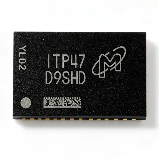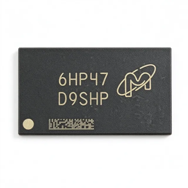
MT41K256M16TW-093 - 4Gbit DDR3L SDRAM 1.066GHz | Micron
MPN: MT41K256M16TW-093 ✓ Active| Qty | Unit Price | Extended |
|---|---|---|
| 1 | $22.23 | $22.23 |
| 10 | $20.5 | $205.00 |
| 100 | $18.75 | $1,875.00 |
| 500 | $17 | $8,500.00 |
| 1,000 | $15.5 | $15,500.00 |
MT41K256M16TW-093 Overview
DDR3L SDRAM (Double Data Rate 3 Low Voltage) is a type of synchronous dynamic random-access memory that transfers data on both edges of the clock, achieving high bandwidth. It is a low-voltage variant of DDR3, operating at 1.35V instead of 1.5V, reducing power consumption by about 15% while maintaining similar performance. DDR3L is part of the DDR SDRAM family, which includes DDR, DDR2, DDR3, and DDR4, each generation offering higher speed and lower power. In a system hierarchy, DDR3L SDRAM sits between the memory controller (often integrated in the CPU or SoC) and the system bus, providing temporary data storage for active processes.
Key features include a 4Gbit density, 16-bit data bus width, 1.35V core voltage, and support for auto self-refresh, auto precharge, asynchronous reset, data mask, dynamic on-chip termination (DTC), ZQ calibration, and write leveling. These features enhance signal integrity and power efficiency, making it suitable for high-performance computing and mobile applications. The device also supports a temperature range of 0°C to +95°C (TC) for standard operation, with an industrial temperature variant available.
Technically, the MT41K256M16TW-093 uses a 30nm-class process technology, enabling high density and low power. It incorporates on-die termination (ODT) to improve signal quality on the memory bus, and its ZQ calibration feature allows precise impedance matching. The device is designed for reliable operation in demanding environments, with a mean time between failures (MTBF) that meets industry standards.
Typical applications include servers, networking equipment, industrial computing, and embedded systems where high memory bandwidth and low power are critical. Its 1.35V operation makes it ideal for power-sensitive designs, such as laptops and portable devices, while its high speed supports data-intensive tasks like real-time analytics and virtualization.
When designing with this component, ensure proper decoupling capacitors are placed near the power pins to minimize noise, and follow the PCB layout guidelines in the datasheet to maintain signal integrity at 2133 MT/s. The device requires a stable 1.35V supply and careful termination of the address/control bus.
Drop-in alternatives for MT41K256M16TW-093 — same package, pin-to-pin compatible. Different-package parts requiring PCB rework are excluded.
Variants in this series
Same-series models that are drop-in compatible with MT41K256M16TW-093 (same form factor and footprint) — differing in Data Bus Width, Data Rate, Package, Supply Voltage.
Quick Comparison Tool — Select alternative parts for side-by-side comparison:
MT41K256M16TW-093:P
✓ In Stock
$15.5 / Unit
View Datasheet →MT41K256M16TW-107:P
✓ In Stock
$16 / Unit
View Datasheet →K4B4G1646E-BYMA
✓ In Stock
$14.3182 / Unit
View Datasheet →MT41K256M16TW-093 IT:P
📋 Reference alternative (not in catalog)
H5AN8G6NAFR-TFC
📋 Reference alternative (not in catalog)
MT41K256M16TW-093 Maximum Ratings & Electrical Characteristics
| Memory Type | DDR3L SDRAM |
| Memory Size | 4Gbit (256M x 16) |
| Data Bus Width | 16 bit |
| Clock Frequency | 1.066 GHz |
| Data Rate | 2133 MT/s |
| Access Time | 20 ns |
| Supply Voltage | 1.35 V (1.283 V to 1.45 V) |
| Interface Type | Parallel |
| Package | 96-FBGA (8x14 mm) |
| Mounting Type | Surface Mount |
| Operating Temperature Range | 0°C to +95°C (TC) |
| RoHS Status | Compliant |
| REACH Status | Compliant |
| Auto Self-Refresh | Yes |
| Auto Precharge | Yes |
| Asynchronous Reset | Yes |
| Data Mask | Yes |
| Dynamic On-Chip Termination | Yes |
| ZQ Calibration | Yes |
| Write Leveling | Yes |
MT41K256M16TW-093 Pin Configuration
| Pin A1 | VDD — Power supply (1.35V) |
| Pin A2 | DQ0 — Data input/output 0 |
| Pin A3 | DQ1 — Data input/output 1 |
| Pin A4 | VSS — Ground |
| Pin A5 | DQ2 — Data input/output 2 |
| Pin A6 | DQ3 — Data input/output 3 |
| Pin A7 | VDDQ — I/O power supply |
| Pin A8 | DQ4 — Data input/output 4 |
| Pin A9 | DQ5 — Data input/output 5 |
| Pin A10 | VSS — Ground |
| Pin A11 | DQ6 — Data input/output 6 |
| Pin A12 | DQ7 — Data input/output 7 |
| Pin B1 | VSS — Ground |
| Pin B2 | DQ8 — Data input/output 8 |
| Pin B3 | DQ9 — Data input/output 9 |
| Pin B4 | VDD — Power supply |
| Pin B5 | DQ10 — Data input/output 10 |
| Pin B6 | DQ11 — Data input/output 11 |
| Pin B7 | VSS — Ground |
| Pin B8 | DQ12 — Data input/output 12 |
| Pin B9 | DQ13 — Data input/output 13 |
| Pin B10 | VDDQ — I/O power supply |
| Pin B11 | DQ14 — Data input/output 14 |
| Pin B12 | DQ15 — Data input/output 15 |
| Pin C1 | VDD — Power supply |
| Pin C2 | A0 — Address input 0 |
| Pin C3 | A1 — Address input 1 |
| Pin C4 | A2 — Address input 2 |
| Pin C5 | A3 — Address input 3 |
| Pin C6 | A4 — Address input 4 |
| Pin C7 | A5 — Address input 5 |
| Pin C8 | A6 — Address input 6 |
| Pin C9 | A7 — Address input 7 |
| Pin C10 | A8 — Address input 8 |
| Pin C11 | A9 — Address input 9 |
| Pin C12 | VSS — Ground |
| Pin D1 | VSS — Ground |
| Pin D2 | A10/AP — Address input 10 / Auto-precharge |
| Pin D3 | A11 — Address input 11 |
| Pin D4 | A12/BC — Address input 12 / Burst chop |
| Pin D5 | A13 — Address input 13 |
| Pin D6 | A14 — Address input 14 |
| Pin D7 | A15 — Address input 15 |
| Pin D8 | BA0 — Bank address 0 |
| Pin D9 | BA1 — Bank address 1 |
| Pin D10 | BA2 — Bank address 2 |
| Pin D11 | RAS# — Row address strobe |
| Pin D12 | VDD — Power supply |
| Pin E1 | VDD — Power supply |
| Pin E2 | CAS# — Column address strobe |
| Pin E3 | WE# — Write enable |
| Pin E4 | CS# — Chip select |
| Pin E5 | CKE — Clock enable |
| Pin E6 | ODT — On-die termination |
| Pin E7 | CK — Clock (positive) |
| Pin E8 | CK# — Clock (negative) |
| Pin E9 | RESET# — Reset |
| Pin E10 | DM0 — Data mask 0 |
| Pin E11 | DM1 — Data mask 1 |
| Pin E12 | VSS — Ground |
| Pin F1 | VSS — Ground |
| Pin F2 | TDQS0 — Termination data strobe 0 |
| Pin F3 | TDQS1 — Termination data strobe 1 |
| Pin F4 | VDDQ — I/O power supply |
| Pin F5 | VDD — Power supply |
| Pin F6 | VSS — Ground |
| Pin F7 | VDDQ — I/O power supply |
| Pin F8 | VDD — Power supply |
| Pin F9 | VSS — Ground |
| Pin F10 | VDDQ — I/O power supply |
| Pin F11 | VDD — Power supply |
| Pin F12 | VSS — Ground |
Typical Applications
MT41K256M16TW-093 is suitable for 6 applications: Server Memory, Networking Equipment, Industrial Computing, Mobile and Portable Devices, Automotive Infotainment, Test and Measurement.
Server Memory
The MT41K256M16TW-093 provides high-density, low-power memory for server applications. Its 4Gbit capacity and 2133 MT/s data rate support demanding workloads such as virtualization and cloud computing. The 1.35V operation reduces power consumption in data centers, contributing to lower operating costs. When used in registered DIMMs, it enables reliable operation in multi-channel configurations, ensuring high throughput for enterprise applications.
Recommended
Networking Equipment
In networking equipment like routers and switches, the MT41K256M16TW-093 offers the speed and capacity needed for packet buffering and forwarding tables. Its 2133 MT/s data rate ensures low latency, while the 1.35V supply helps manage thermal budgets in compact enclosures. The device's on-die termination and ZQ calibration improve signal integrity on high-speed buses, making it suitable for 10GbE and 40GbE line cards.
Recommended
Industrial Computing
For industrial PCs and embedded systems, the MT41K256M16TW-093 provides reliable memory in harsh environments. Its operating temperature range of 0°C to +95°C (TC) covers most industrial settings, and the industrial temperature variant extends this to -40°C. The low-voltage operation reduces heat generation, which is critical in sealed enclosures. The device's robust design ensures long-term reliability in factory automation and process control.
Recommended
Mobile and Portable Devices
The MT41K256M16TW-093's 1.35V operation makes it ideal for battery-powered devices, reducing power consumption by up to 15% compared to standard DDR3. Its 4Gbit density supports multitasking and multimedia applications in smartphones, tablets, and ultrabooks. The small 96-FBGA package saves board space, and the auto self-refresh feature minimizes standby power, extending battery life.
Recommended
Automotive Infotainment
In automotive infotainment systems, the MT41K256M16TW-093 provides the memory bandwidth for navigation, audio, and video playback. Its high data rate ensures smooth graphics rendering, while the low-voltage operation helps manage the thermal environment inside the vehicle. The device's reliability and long lifecycle support automotive-grade requirements, and the industrial temperature variant can handle extreme temperatures. It is suitable for head units and telematics systems.
Recommended
Test and Measurement
The MT41K256M16TW-093 is used in test and measurement equipment such as oscilloscopes and logic analyzers, where high-speed data acquisition requires fast memory. Its 2133 MT/s data rate enables real-time signal processing, and the 4Gbit capacity allows for long capture buffers. The device's low power consumption is beneficial in portable instruments, and its precise timing characteristics ensure accurate data capture.
Recommended
Recommended Products Summary
Engineering reference data for MT41K256M16TW-093 — comparison, design guidance, and compliance information.
Selection Guide
Comparison with Alternatives
| Parameter | This Product | MT41K256M16TW-093 | MT41K256M16TW-093 IT | MT41K256M16TW-107 | K4B4G1646E-BYMA | H5AN8G6NAFR-TFC |
|---|---|---|---|---|---|---|
| Package | 96-FBGA (8x14 mm) | P: 96-FBGA (8x14 mm) | P: 96-FBGA (8x14 mm) | P: 96-FBGA (8x14 mm) | 96-FBGA (8x14 mm) | 96-FBGA (8x14 mm) |
| Brand | Micron Technology | P: Micron Technology | P: Micron Technology | P: Micron Technology | Samsung Electronics | SK Hynix |
| Memory Size | 4Gbit | P: 4Gbit | P: 4Gbit | P: 4Gbit | 4Gbit | 4Gbit |
| Data Rate | 2133 MT/s | P: 2133 MT/s | P: 2133 MT/s | P: 1866 MT/s | 2133 MT/s | 2133 MT/s |
| Supply Voltage | 1.35V | P: 1.35V | P: 1.35V | P: 1.35V | 1.35V | 1.35V |
| Operating Temperature | 0°C to +95°C | P: 0°C to +95°C | P: -40°C to +95°C | P: 0°C to +95°C | 0°C to +95°C | 0°C to +95°C |
| RoHS | Compliant | P: Compliant | P: Compliant | P: Compliant | Compliant | Compliant |
Key Differentiators
- Higher speed grade than -107 variant (vs MT41K256M16TW-107:P)
- Industrial temperature option (vs K4B4G1646E-BYMA)
- Low-voltage operation (vs H5AN8G6NAFR-TFC)
Design Notes
For reliable operation at 2133 MT/s, maintain controlled impedance of 50 ohms for data lines and 40 ohms for address/command lines. Keep trace lengths matched within +/- 0.5 mm to minimize skew. Use a solid ground plane beneath the memory device and place decoupling capacitors (0.1uF and 1uF) close to each VDD and VDDQ pin.
The MT41K256M16TW-093 dissipates up to 1.5W under full load. Ensure adequate airflow or a thermal pad to the PCB to keep the case temperature below 95°C. For industrial temperature variants, the maximum case temperature is 95°C, but ambient may be higher; consider heatsinking if the device is in a confined space.
Use on-die termination (ODT) settings as recommended in the datasheet to match the motherboard's impedance. Enable ZQ calibration during initialization to compensate for process variations. For high-speed signals, route data lines on inner layers with ground shielding to reduce crosstalk and EMI.
Compliance Information
RoHS and REACH compliant per distributor listings. Not AEC-Q100 qualified as it is a memory component.