Memory ICs
Subcategories
Products (459)
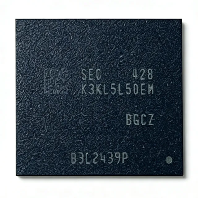
K3KL4L40EM-BGCU - 12GB LPDDR5X DRAM 8533Mbps | Samsung
The Samsung K3KL4L40EM-BGCU is a 96 Gbit (12 GB) LPDDR5X low-power DRAM device with a 64-bit bus operating at data rates up to 8,533 Mbps, housed in a 496-ball FBGA package. LPDDR5X (Low Power Double Data Rate 5X) is an extension of the JEDEC LPDDR5 standard that pushes the data rate ceiling beyond LPDDR5's 6,400 Mbps while lowering supply voltage for reduced power consumption. As a class of volatile memory in the DRAM hierarchy, LPDDR5X serves as the main system memory in mobile SoC platforms, sitting alongside application processors such as Qualcomm Snapdragon and MediaTek Dimensity where bandwidth-per-watt is the dominant design metric. Key features of the K3KL4L40EM-BGCU include its 96 Gbit density (single-die 12 GB organization), an x64 bus width, and an industry-leading 8,533 Mbps maximum data rate. The ultra-low-power mobile DRAM design targets energy efficiency, which directly extends battery life in handheld and wearable products. The 496-ball FBGA (Fine-Pitch Ball Grid Array) package provides a compact footprint for dense mobile PCBs. Architecturally, the device belongs to Samsung's LPDDR5X family alongside the 64 Gbit K3KL3L30DM-BGCU and 128 Gbit K3KL5L50DM-BGCU, all sharing the same 496 FBGA footprint and 8,533 Mbps speed grade. This density-family structure allows platform vendors to scale memory capacity between 8 GB, 12 GB, and 16 GB total configurations (with stacked or multi-die assemblies) without changing PCB layout or signal-integrity design. Typical applications include flagship smartphones paired with Snapdragon-class CPUs, tablets, wearables, and edge-AI computing modules where high memory bandwidth is needed for on-device inference. Design consideration: LPDDR5X signal integrity at 8,533 Mbps demands strict length-matched routing, controlled impedance, and following the SoC vendor's reference layout guidelines. This page synthesizes distributor stock data, drop-in density alternatives, and practical design notes not found in the manufacturer datasheet. Pricing and stock references are as of 2026-09-04.

K3KL7L70EM-MGCU - 12Gb LPDDR5X DRAM, 315-ball | Samsung
The Samsung K3KL7L70EM-MGCU is a 12 Gigabit LPDDR5X (Low Power Double Data Rate 5X) SDRAM device in a 315-ball FBGA (Fine-Pitch Ball Grid Array) package, organized x32 and in mass production status. LPDDR5X is the low-power synchronous DRAM standard evolved from LPDDR5, targeting mobile and edge-computing systems where bandwidth-per-watt is the dominant design constraint. In the memory hierarchy, DRAM sits between CPU caches and non-volatile storage (NAND flash, UFS, eMMC), serving as the primary working memory for application processors, AI accelerators, and SoCs. LPDDR5X raises the LPDDR5 interface speed ceiling while reducing operating voltage, delivering higher data rates at lower power than its predecessor. Key features of the K3KL7L70EM-MGCU include its 12 Gbit density, a x32 memory organization suited to wide-bus mobile and embedded SoC integration, and the compact 315-ball FBGA footprint standard for LPDDR5X class devices. Samsung produces this device at high volume (Johor, Malaysia is listed as one fab location for the family), which supports long-term supply for smartphone, tablet, automotive infotainment, and AI edge module designers. Architecturally, LPDDR5X devices use dynamic voltage/frequency scaling with multiple power modes (deep sleep, self refresh) to minimize standby current in battery-powered systems. The interface supports bank group architectures and burst access optimized for real-time multimedia and neural-network workloads. Typical applications include flagship smartphone main memory, AI edge compute modules, automotive digital cockpits and ADAS platforms, and high-bandwidth embedded systems that pair LPDDR5X with Qualcomm or MediaTek application processors. When designing with this part, signal integrity of the high-speed command/address/data bus is the dominant engineering challenge: matched-length fly-by routing, per-byte termination control, and SoC memory-controller training routines are essential for reliable operation at LPDDR5X data rates. This page synthesizes verified distributor data, package and organization details, sourcing information, and practical design context not consolidated in any single datasheet listing.
K3KL8L80CM-MGCT - 32Gb LPDDR5X SDRAM x32 | Samsung
The Samsung K3KL8L80CM-MGCT is a 32 Gbit (4 GB) LPDDR5X SDRAM with a 32-bit (x32) data bus, supplied in a 315-ball FBGA package. It operates from -25C to +85C with core power at 1.05V and support rails at 500 mV (VDDQ low-power mode), 900 mV (VDDQ), and 1.8V (VDD2), delivering data rates up to 7500 Mbps for high-bandwidth, power-constrained designs. LPDDR5X (Low Power Double Data Rate 5X) is a JEDEC-defined evolution of the LPDDR5 DRAM standard that extends interface speed while lowering the I/O supply voltage. Within the memory hierarchy, LPDDR5X sits in the low-power DRAM family alongside LPDDR4X and LPDDR5, targeting mobile SoCs, embedded platforms, and increasingly automotive and on-device AI processors where bandwidth per watt matters more than raw capacity expansion. Key features of the K3KL8L80CM include the LPDDR5X interface with speeds up to 7500 Mbps, a wide x32 organization suited to single-channel or stacked multi-die designs, and Samsung's power-efficiency improvements of roughly 20-25% versus the previous LPDDR5 generation. The FBGA-315 ball map follows the standard LPDDR5/LPDDR5X monolithic die footprint used across Samsung's K3KL family. Architecturally, the device uses Samsung advanced DRAM process technology with dynamic voltage scaling of the VDDQ rail down to approximately 500 mV in deep power-down and low-frequency states, plus per-bank and deep-sleep power-down modes that cut idle current dramatically - critical for battery-powered and thermally constrained systems. Typical applications include flagship smartphone and tablet main memory, AI edge accelerators and on-device inference modules, automotive infotainment and ADAS compute platforms, and embedded single-board computers. Design consideration: LPDDR5X signal integrity demands careful length-matched routing, on-die termination configuration through mode registers, and a clean 1.05V core rail with low-ESR decoupling; verify controller compatibility with the target 7500 Mbps rate bin before layout. This page synthesizes distributor pricing, cross-reference alternatives, and practical design notes not found in the Samsung datasheet.
K3KL8L80DM-JGCT - 32Gb LPDDR5X DRAM FBGA-315 | Samsung
The Samsung K3KL8L80DM-JGCT is a 32 Gbit (4 GB) LPDDR5X SDRAM device organized x32 in a 315-ball FBGA (BGA-315) package, part of Samsung's LPDDR5X DRAM family supporting data rates of up to 7,500-8,500 Mbps with roughly 20-25% better power efficiency than LPDDR5. LPDDR5X (Low Power Double Data Rate 5X) is an enhanced, low-power SDRAM interface standard used as main memory in battery-powered and thermally constrained systems. Within the memory hierarchy it belongs to the DRAM family -> synchronous DRAM -> LPDDR -> LPDDR5X, and it differs from DDR5 server DRAM by optimizing power per bit transfer rather than peak channel density. Key features include the 32 Gbit monolithic die density, an x32 data organization suited to mobile application processors, multi-rail operation (VDD1/VDD2/VDDQ at approximately 1.8 V, 1.05 V, 0.9 V and 0.5 V class rails per the LPDDR5X generation), and operation over -25 C to +85 C. The FBGA-315 package provides low-inductance ball interconnects for multi-gigabit signaling. Architecturally, LPDDR5X builds on LPDDR5 with enhanced speed-binned operation, dynamic voltage scaling, deep sleep modes, and link ECC features that reduce refresh power and preserve data integrity in always-on AI workloads. Typical applications are flagship smartphone and tablet main memory, on-device AI accelerators, automotive infotainment and ADAS domains, and compact PC/edge modules. Design consideration: LPDDR5X signal integrity requires careful length-matched routing, on-die termination tuning, and controller training; verify the exact speed grade suffix against the JEDEC LPDDR5X-compatible controller spec before layout. This page adds distributor availability signals, same-family drop-in alternatives, and design guidance synthesized beyond the raw Samsung datasheet.
K3KL8L80DM-MGCU - 8Gb LPDDR5X DRAM 1Gx32 | Samsung
The Samsung K3KL8L80DM-MGCU is an 8 Gbit LPDDR5X SDRAM organized as 1G x 32, operating from a nominal 1.05 V supply and packaged in a 315-ball FBGA (fine-pitch ball grid array) surface-mount package. As an LPDDR5X device, it delivers the highest-bandwidth, lowest-power mobile DRAM performance in Samsung's portfolio, targeting flagship smartphone, tablet, automotive infotainment, and AI edge-computing platforms. LPDDR (Low Power Double Data Rate) SDRAM is a class of memory optimized for mobile and battery-powered systems, sitting within the broader DRAM -> synchronous DRAM -> memory IC -> semiconductor hierarchy. LPDDR5X extends the LPDDR5 JEDEC architecture with higher data rates and improved power efficiency, making it the dominant main-memory technology for mobile SoCs from Qualcomm, MediaTek, and Samsung Exynos. Key features of this device include the 8 Gbit density in a single-die 1G x 32 organization, the LPDDR5X interface with substantially higher transfer rates than LPDDR5, and the compact FBGA-315 footprint used across Samsung's 315-ball LPDDR5X family. Samsung LPDDR5X devices also support advanced power-management features inherited from LPDDR5, including Deep Sleep Mode and per-bank refresh, which reduce idle power in always-on mobile workloads. Architecturally, the die integrates Samsung's advanced DRAM process technology with LPDDR5X I/O that supports dynamic voltage and frequency scaling. The x32 organization simplifies main-memory subsystem design for SoCs requiring 32-bit or wider buses in PoP (Package-on-Package) or discrete-memory configurations, and multiple devices can be stacked or channel-interleaved to widen the memory bus. Typical applications include flagship smartphone main memory, tablet and notebook LPDDR subsystems, automotive cockpit and ADAS compute platforms, and edge-AI accelerator boards where high bandwidth per watt is the primary selection criterion. When designing with this part, verify SoC LPDDR5X controller compatibility, speed-grade suffix, and the exact 315-ball ball-map before committing the PCB footprint, since Samsung suffix codes encode speed and configuration differences that are not mechanically interchangeable. This page synthesizes distributor sourcing data, same-family Samsung alternatives, and procurement guidance not found in the manufacturer datasheet.

K3KL8L80QM-MUCT - 32Gb LPDDR5X DRAM | Samsung
The Samsung Electronics K3KL8L80QM-MUCT is a 32 Gigabit (4 GB) LPDDR5X DRAM memory chip from Samsung's LPDDR5X family, fabricated on Samsung advanced DRAM process technology and housed in an original-package fine-pitch ball grid array (FBGA, 315-ball class) surface-mount package. The part is a core memory component for flagship smartphones, AI edge computing modules, and high-bandwidth portable systems. LPDDR (Low Power Double Data Rate) SDRAM is a class of mobile DRAM optimized for high bandwidth at low power. Within the memory hierarchy, LPDDR5X sits above LPDDR5 and LPDDR4X as a next-generation low-power DRAM type, belonging to the broader DRAM -> semiconductor memory -> semiconductor taxonomy. LPDDR5X increases I/O speed over LPDDR5 while lowering operating voltage, delivering higher bandwidth per watt - a critical metric for battery-powered AI workloads. Key characteristics of the K3KL8L80QM-MUCT include its 32 Gb (4 GB) monolithic density, LPDDR5X interface with data rates in the multi-gigabit-per-second class per pin, and a low-voltage core/IO power architecture typical of the LPDDR5X standard. The QM speed grade and MUCT packaging suffix encode speed bin, operating temperature class, and packing format used across Samsung mobile DRAM numbering. Architecturally, the device is organized as a DRAM array accessed through a high-speed LPDDR5X channel interface with burst-oriented operation, bank-group parallelism, and dynamic voltage/frequency scaling features. Samsung implements on-die termination and training features required by the LPDDR5X protocol to maintain signal integrity at the elevated data rates. Typical applications include flagship smartphone AP memory (paired with Snapdragon or Exynos application processors), AI accelerator companion memory in edge modules, automotive infotainment memory subsystems, and high-performance portable computing devices such as tablets and 5G modems. A key design consideration: LPDDR5X signal integrity demands strict length matching, on-die termination tuning, and reference-plane-continuous PCB stackup; memory controller firmware must support LPDDR5X training sequences. This page synthesizes distributor sourcing data, same-family drop-in alternatives, and practical design notes not found in a single manufacturer document, streamlining procurement and second-source planning for this memory IC.
K3KL9L90DM-JGCT - LPDDR5X DRAM 16Gbit FBGA-315 | Samsung
The Samsung K3KL9L90DM-JGCT is a 16Gbit LPDDR5X low-power DRAM SDRAM memory component from Samsung Electronics, housed in a 315-ball FBGA (fine-pitch ball grid array) package. As part of Samsung's LPDDR5X family, it targets premium mobile, automotive, and IT applications requiring high memory bandwidth with low power consumption; Samsung's LPDDR5X portfolio provides data rates up to 8.5 Gbps with approximately 20% better power efficiency than LPDDR5. LPDDR (Low Power Double Data Rate) SDRAM is a class of DRAM optimized for power-sensitive systems such as smartphones, tablets, edge-AI accelerators, and automotive infotainment. Sitting within the memory IC hierarchy (DRAM -> SDRAM -> LPDDR family -> LPDDR5X), LPDDR5X devices use a low-voltage interface, deep power-down modes, and advanced bank architectures to maximize bandwidth-per-watt. Key characteristics of this device include its 16Gbit density per package, FBGA-315 surface-mount package, and an operating temperature range documented at -25C to +85C for family devices. The LPDDR5X interface supports channelized architecture and dynamic voltage/frequency scaling for workload-adaptive power management. Technically, LPDDR5X devices implement CA training, DFE (decision feedback equalization) on data reads, and link ECC options to sustain multi-gigabit-per-second signaling on PCB traces. Signal integrity on fly-by command/address buses and length-matched data lanes are critical to achieving rated speeds. Typical applications include flagship smartphone application-processor memory, automotive ADAS domain controllers, AI edge inference modules, and high-performance mobile computing platforms such as tablets and XR headsets. Design consideration: LPDDR5X routing requires strict length matching and impedance control; consult the Samsung LPDDR5X design guide and SoC memory-controller initialization sequences before layout. This page synthesizes verified distributor data, family cross-references, and practical design notes not found in a single datasheet source.
K3KL9L90DM-MGCU - LPDDR5X 64Gb x32 8533Mbps FBGA | Samsung
The Samsung K3KL9L90DM-MGCU is an LPDDR5X SDRAM memory device offering 64 Gbit total density (8 GB) organized as x32, operating at data rates up to 8533 Mbps per pin, packaged in a 315-ball FBGA (fine-pitch ball grid array) surface-mount package rated for -25C to +85C operation. LPDDR5X (Low Power Double Data Rate 5X) is the JEDEC-defined evolution of the LPDDR5 standard, extending the data-rate ceiling far beyond LPDDR5 while retaining low-voltage signaling for battery-powered and thermally constrained platforms. In the memory hierarchy it sits as a synchronous DRAM directly soldered onto the host PCB (memory -> DRAM -> SDRAM -> LPDDR family), typically paired with application processors or SoCs in smartphones, tablets, AI edge devices, and automotive infotainment systems. Key features of the K3KL9L90DM-MGCU include its 8533 Mbps pin speed, which places it at the top of the LPDDR5X speed grade ladder and delivers class-leading bandwidth for memory-hungry AI inference and high-refresh-rate display workloads; its 32-bit-wide channel organization, which simplifies single-channel SoC integrations; and the compact 315-ball FBGA footprint that conserves PCB area in dense mobile designs. Samsung is the volume leader in LPDRAM manufacturing, and this part belongs to Samsung's 10nm-class LPDDR5X family used across flagship mobile platforms. Architecturally, the device uses LPDDR5X low-voltage I/O signaling and dynamic voltage/frequency scaling governed by the JEDEC LPDDR5X protocol, allowing the memory controller to trade speed against power in real time. Deep power-down and partial-array self-refresh modes minimize standby drain in always-on scenarios such as voice wakeup and background sensing. Typical applications include flagship smartphone main memory, AI edge accelerator buffering, automotive infotainment and ADAS perception platforms, and high-performance embedded computing modules where soldered-down memory yields better signal integrity and lower profile than SODIMM-based solutions. A key design consideration: LPDDR5X routing at 8533 Mbps demands strict length matching, reference-plane integrity, and eye-diagram validation on the CA/CK/DQ nets; the memory controller and PHY must also support the exact speed grade and training sequences. This page synthesizes distributor pricing, drop-in alternatives, and practical design notes not found in the manufacturer datasheet.
K3KLALA0DM-JGCT - LPDDR5X DRAM x32 | Samsung Semiconductor
The Samsung Semiconductor K3KLALA0DM-JGCT is an LPDDR5X (Low Power Double Data Rate 5X) DRAM memory IC in a x32 organization, produced by Samsung Electronics in mass production status. Samsung's LPDDR5X family delivers data rates of up to 8.5 Gbps per pin with approximately 20% better power efficiency than LPDDR5, and densities ranging up to 64 GB per package in the broader family portfolio. LPDDR5X is a premium low-power DRAM standard evolved from the LPDDR (Low Power Double Data Rate) lineage: LPDDR -> LPDDR4X -> LPDDR5 -> LPDDR5X. It belongs to the volatile memory -> DRAM -> synchronous DRAM hierarchy and serves as the main-system-memory workhorse in devices where bandwidth per watt is the dominant constraint. Unlike DDR5 DIMM memory used in servers, LPDDR5X is soldered directly onto the PCB as a discrete BGA package. Key characteristics of this family include high-speed data processing (up to 8.5 Gbps on leading speed grades), aggressive power scaling with dynamic voltage/frequency switching, and deep sleep states that minimize standby current in battery-operated systems. The x32 organization provides wide parallelism that reduces bus clock requirements for a given aggregate bandwidth. Architecturally, LPDDR5X extends LPDDR5 by operating the command/address and data interface at higher signaling rates with enhanced signal-integrity training, link ECC options, and refined DVFSC/DVFSP (dynamic voltage and frequency scaling center/point) features. Memory controllers must support the JEDEC LPDDR5X mode registers to exploit the extended speed bins. Typical applications include flagship smartphone and tablet main memory, AI edge computing accelerators, automotive infotainment and ADAS domain controllers, and high-performance embedded systems. Design consideration: LPDDR5X routing demands careful length matching, impedance control, and reference to the manufacturer's layout guidelines; controller and PHY compatibility with the exact speed bin must be verified before layout freeze. This page synthesizes distributor sourcing data, same-family drop-in alternatives, and practical design notes not found in a single manufacturer datasheet.
K3KLALA0DM-MGCU - 16Gb LPDDR5X DRAM 6400Mbps | Samsung
The Samsung K3KLALA0DM-MGCU is a 16 Gigabit LPDDR5X (Low Power Double Data Rate 5X) SDRAM die operating at up to 6400 Mbps per pin, housed in a 315-ball FBGA package for mobile and ultra-compact computing platforms. LPDDR5X is a low-power synchronous DRAM interface standard that extends LPDDR5 with higher data rates and improved signal integrity for battery-powered systems. In the memory hierarchy, it sits as a DRAM device serving as main system memory, positioned below storage (UFS, eMMC, NAND) and above SRAM caches. LPDDR5X devices use a low-voltage signaling interface (VDDQ around 0.5 V class for the 6400 Mbps speed grade) and channel architectures optimized for bandwidth-per-watt in smartphones, tablets, and AI edge accelerators. Key characteristics of this part include its 16 Gbit density per die, a 6400 Mbps maximum data rate, and the 315-ball FBGA footprint that is the standard LPDDR5/LPDDR5X die-scale package. The MGCU speed-grade suffix in Samsung's naming convention identifies the LPDDR5X 6400 Mbps-class device, and the device is sourced from Samsung's advanced DRAM process with EUV-lithography cell technology, which improves bit density and reduces power per bit transfer. Technically, LPDDR5X devices such as this one use WCK (word clock) architecture with CA bus training, on-die termination, and link ECC features to sustain multi-gigabit signaling across the mobile-grade channel. The die is designed to attach into package-on-package or PoP-less MCP/uMCP stacks, and Samsung ships these dies both as discrete FBGA components and inside uMCP solutions for handset platforms. Typical applications include flagship smartphone main memory, tablet and notebook (always-connected PC) DRAM, automotive infotainment memory, and AI edge compute modules where LPDDR5X bandwidth is required within a strict power envelope. A key design consideration is signal integrity: at 6400 Mbps, PCB trace length matching, WCK routing, and CA bus termination must follow the LPDDR5X JEDEC-class layout guidance, and SoC memory-controller compatibility for LPDDR5X speed grades should be confirmed before BOM placement. This page adds value beyond the Samsung product listing by synthesizing distributor sourcing channels, same-family drop-in alternatives, and application-level design context not found in any single source.

K3KLELE0DM-BGCU - 144Gb LPDDR5X 8533Mbps DRAM | Samsung
The Samsung K3KLELE0DM-BGCU is a 144 Gb LPDDR5X (Low Power Double Data Rate 5X) DRAM memory IC organized x64, delivering data rates up to 8533 Mbps across a 496-ball FBGA package, with multi-rail supply voltages of 1.8 V, 1.05 V, 0.9 V and 0.5 V and an operating temperature range of -25 to +85 C. LPDDR5X is the premium tier of the low-power DRAM family, which sits within the broader DRAM -> volatile memory -> semiconductor memory hierarchy. Unlike DDR5 server DRAM, LPDDR5X is architected for bandwidth-per-watt: it attaches directly to the host SoC in a point-to-point topology on the same PCB, eliminating DIMM connectors and reducing trace length and load. Key features include the 144 Gb density (18 GB equivalent when used in x64 organization per die stack), the 8533 Mbps pin speed, which Samsung states is approximately 1.25 times faster than the previous LPDDR generation, and about 25% better power efficiency enabled by lower core voltage and advanced I/O calibration. The multi-voltage architecture separates core (0.5 V region), I/O and interface rails for fine-grained power management. Technically, LPDDR5X uses sophisticated training, DFE (decision feedback equalization) on reads, and per-byte write CRC to sustain 8533 Mbps signaling integrity. Bank-group and deep-bank organization reduce row-conflict latency for AI workloads. Typical applications include AI accelerators and edge AI modules, premium smartphones and tablets, automotive infotainment and ADAS platforms, and high-performance embedded computing where memory bandwidth per watt is the limiting factor. Design consideration: the part is marked EOL by the source listing, so new designs should plan lifecycle management or dual-source qualification; verify availability before committing to production. This page synthesizes distributor stock listings, spec aggregation, and drop-in alternatives not found in a single manufacturer datasheet.

K3LK2K20CM-JFCP - 48Gb LPDDR5 DRAM 441ball | Samsung
The Samsung K3LK2K20CM-JFCP is a 48Gbit LPDDR5 SDRAM memory IC fabricated by Samsung Electronics, organized with a data rate of LPDDR5-5500 and housed in a 441-ball FBGA package. It belongs to Samsung's K3LK2K20CM LPDDR5 family, delivering high-bandwidth mobile DRAM for next-generation applications with pin speeds up to 6,400 Mbps and up to 20% power savings versus LPDDR4X. LPDDR5 (Low Power Double Data Rate 5) is a JEDEC-defined low-power DRAM interface standard used where memory bandwidth must be maximized while power draw is minimized. In the system hierarchy, it sits as DRAM -> synchronous DRAM -> low-power SDRAM -> LPDDR5, typically serving as the main system memory in SoC-based platforms. Compared with LPDDR4X, LPDDR5 adds bank group architecture improvements, deeper sleep modes, and a WCK/flexible clocking scheme that enables the 5500 Mbps-class data rates seen in this part. Key features of the K3LK2K20CM-JFCP include 48Gbit density (6 GB per device), LPDDR5-5500 speed grade, the 441-ball FBGA footprint shared across the CM speed-tier variants, and Samsung's volume mobile DRAM manufacturing. The -JFCP suffix identifies the speed/binning and package-code combination within the family; sibling codes such as -BGCP, -JHCP and -JUCP share the same 441-ball LPDDR5 package with different speed or binning grades. From a technical perspective, LPDDR5 devices like this one use a low-voltage interface (VDDQ of the LPDDR5 generation) and bank-group parallelism to sustain high throughput per channel. Mobile SoC memory controllers from Qualcomm and MediaTek platforms are commonly paired with Samsung LPDDR5 at 51.2 GB/s aggregate transfer rates for the widest configurations. Typical applications include flagship smartphone main memory, tablet and notebook SoC memory, automotive infotainment processors, AI edge computing modules, and 5G networking equipment where high bandwidth per watt is critical. A key design consideration: LPDDR5 signal integrity demands strict length-matched routing, on-die termination tuning, and careful VDDQ rail decoupling; the 441-ball BGA requires controlled-impedance PCB stackups. This page synthesizes distributor sourcing data, family cross-references, and drop-in variant analysis not found in a single manufacturer datasheet.
K3LK3L30CM-BGCU - 64Gb LPDDR5X DRAM 8533Mbps | Samsung
The Samsung Semiconductor K3LK3L30CM-BGCU is a 64 Gb LPDDR5X low-power DRAM with data rates up to 8533 Mbps, housed in a 496-ball FBGA (BGC) package optimized for mobile and edge-AI SoC integration. According to Samsung product information, this premium low-power DRAM delivers speeds up to 1.25x faster and approximately 25% better power efficiency than the previous LPDDR generation. LPDDR5X (Low Power Double Data Rate 5X) is a JEDEC-classified low-power synchronous DRAM interface standard descended from the LPDDR family: LPDDR -> LPDDR4/4X -> LPDDR5 -> LPDDR5X. Its role in the system hierarchy is as the main system memory for battery-powered, thermally constrained SoC platforms such as smartphone application processors, automotive infinisics, and AI edge accelerators, where bandwidth per watt matters more than raw capacity per module. Key features of the K3LK3L30CM-BGCU include 64 Gb (8 GB) of stacked DRAM die in a single compact package, an 8533 Mbps pin speed that yields very high aggregate bandwidth on wide x32-class buses, and low-voltage LPDDR5X signaling (VDDQ of 0.39 V class per the LPDDR5X standard family) that reduces dynamic power. The multi-die stacking technology maximizes density while preserving a mobile-friendly footprint. Technically, the device implements LPDDR5X bank-group architecture with on-die termination, deep power-down and self-refresh power states, and dynamic voltage/frequency scaling so the memory controller can trade bandwidth against power in real time. The 496-ball FBGA ball map follows Samsung's LPDDR5X channel organization for direct connection to compatible mobile SoCs. Typical applications include AI and in-vehicle edge devices (per Samsung's positioning of LPDDR5X), flagship smartphone SoC memory, and high-bandwidth mobile computing platforms. The 25% power-efficiency gain directly extends battery life in these systems. Design consideration: LPDDR5X signal integrity at 8533 Mbps requires strict length-matched routing, on-die termination configuration, and SoC-side controller training; verify Samsung's package ball map against your SoC memory controller before layout. This page synthesizes distributor stock and pricing data, drop-in alternatives, and design guidance not found in the manufacturer datasheet.
K3LK4K40CM-BGCP - LPDDR5 96Gb 6400Mbps DRAM | Samsung
The Samsung Electronics K3LK4K40CM-BGCP is a high-density LPDDR5 SDRAM memory IC offering 96 Gb (12 GB) of DRAM in a 496-ball FBGA package operating at a core supply of 1.05 V with a data rate of up to 6400 Mbps per pin. LPDDR5 (Low Power Double Data Rate 5) is the fifth generation of JEDEC low-power synchronous DRAM aimed at mobile and embedded systems. Within the memory hierarchy it sits under DRAM -> synchronous DRAM -> low-power SDRAM -> LPDDR5, and it serves as the main working memory in smartphones, tablets, and computing modules where bandwidth-per-watt matters more than absolute capacity. Key features of the K3LK4K40CM-BGCP include its 96 Gb density organized as x64 (1536M x 64 per the FBGA-496 listing), 6400 Mbps peak data rate, and a reduced-voltage core rail of 1.05 V that lowers dynamic power versus earlier LPDDR4 generations. Deep power-down modes and per-bank refresh architecture further cut idle current in battery-powered designs. Technically, LPDDR5 introduces bank-group architectures, a 16n prefetch scheme, and flexible on-die termination that allow the interface to scale past 6000 Mbps while preserving signal integrity over mobile-style point-to-point links. Samsung fabricates these devices on advanced DRAM process nodes, and the BGCP suffix denotes the 496-ball FBGA footprint used across the K3LK LPDDR5 family. Typical applications include flagship smartphone and tablet main memory, AI edge accelerators, embedded computing modules, industrial controllers with data logging, and replacement sourcing for uMCP assembly lines. Designers should note that LPDDR5 point-to-point routing requires careful length matching and reference-plane discipline; the memory controller must support the LPDDR5 JEDEC command set, as LPDDR4 controllers are not electrically compatible. This page synthesizes distributor pricing tiers, drop-in family alternatives, and practical design notes not found in the manufacturer datasheet.
K3LK4L40DM-BGCT - Samsung DRAM Memory IC | Samsung Electronics
The Samsung Electronics K3LK4L40DM-BGCT is a DRAM (dynamic random access memory) semiconductor component supplied in a ball grid array (BGA) package, classified by distributors under specialized memory ICs and used across mobile devices, consumer electronics, and embedded systems. Pricing references from third-party spot-market distributors have listed this part at approximately $50.60 per unit for single-piece quantities (as of 2026-09-04). DRAM is the workhorse memory technology of modern electronics: it stores each bit as a charge on a capacitor within a transistor-capacitor cell, providing high density and fast random access at low cost per gigabyte, but requiring periodic refresh to retain data. Within the memory hierarchy, DRAM sits between CPU caches (SRAM) and non-volatile storage (NAND flash), serving as the main working memory in smartphones, tablets, networking equipment, industrial controllers, and PCs. A DRAM component such as this is the building block from which memory modules (DIMMs) and stacked memory subsystems are assembled. Samsung Electronics is the world's largest DRAM manufacturer, and this part follows Samsung's structured naming convention where the K-prefix identifies DRAM products and the -BGCT suffix denotes a BGA-packaged, lead-free (G = RoHS-compliant green) commercial temperature offering. Key selection parameters for DRAM components include density, bus width, data rate, operating voltage class, and package ball count; buyers should consult the manufacturer datasheet for the exact values of these parameters for this ordering code. Typical applications include mobile device main memory, consumer electronics such as smart TVs and set-top boxes, and embedded systems including industrial HMI and networking platforms where dense, high-bandwidth volatile memory is required alongside an application processor or SoC with a compatible memory controller. When designing in this component, verify that your memory controller timing settings (CAS latency, burst length, refresh interval) match the datasheet speed grade, and follow Samsung's layout guidelines for fly-by/daisy-chain routing and VDDQ decoupling. Signal integrity at high data rates demands controlled impedance and length-matched traces. This page synthesizes distributor pricing references, drop-in alternatives, and practical design notes not found in the manufacturer datasheet, giving engineers a single citation-ready resource.
K3LK8K80CM-MFCP - 48Gbit LPDDR5 6400Mbps DRAM | Samsung
The Samsung K3LK8K80CM-MFCP is a 48Gbit LPDDR5 (Low Power Double Data Rate 5) SDRAM memory IC delivering up to 6400 Mbps pin speed, housed in a 315-ball FBGA (MFCP) package. It belongs to Samsung's LPDDR5 DRAM family, which achieves a massive 51.2 GB/s of bandwidth per package and roughly 20% power savings over LPDDR4X. LPDDR5 is the fifth generation of low-power synchronous DRAM defined for mobile, automotive, and edge-computing systems. In the memory hierarchy it sits as the main working memory (DRAM) downstream of the SoC, complementing NAND storage (eMMC, UFS) that holds persistent data. LPDDR5 introduces clocking and data-replication features that let the DRAM operate at a lower core frequency while maintaining the same effective data rate, cutting dynamic power. Key features of the K3LK8K80CM-MFCP include 6400 Mbps pin speed for high-bandwidth SoC interfaces, the compact 315-ball LPDDR5 FBGA footprint used by flagship application processors, and low-voltage signaling that reduces interface power versus previous generations. This variant is specified as an automotive-grade storage chip with an operating temperature range of -40 C to +105 C, making it suitable for vehicle domains where consumer LPDDR5 would not survive. Samsung fabricates LPDDR5 on advanced DRAM process nodes, and this MPN originates from Johor, Malaysia per distributor listings. Typical applications include automotive ADAS and infotainment main memory, 5G smartphone and modem memory buffers, AI edge accelerators, and high-performance portable compute. A memory controller with LPDDR5 support and proper signal-integrity-aware PCB routing is required. Design consideration: LPDDR5 Fly-By/DQ signaling demands length-matched traces, on-die termination settings in the controller, and compliance with VDDQ voltage rails; consult the Samsung LPDDR5 design guide for power sequencing. This page synthesizes distributor pricing leads, family cross-references, and practical design notes not found in a single manufacturer datasheet.
K3LK8L80CM-MGCT - LPDDR5X 32Gbit DRAM FBGA-315 | Samsung
The Samsung K3LK8L80CM-MGCT is a 32 Gbit (4 GB) x32 LPDDR5X SDRAM die packaged in a 315-ball Fine-Pitch Ball Grid Array (FBGA-315), operating from a 0.5 V (VDDQ core domain per JESD8-xx low-voltage signaling) / 1.05 V / 1.8 V multi-rail supply with data rates up to 7500 Mbps for high-bandwidth mobile and on-device AI memory subsystems. LPDDR5X (Low Power Double Data Rate 5 eXtended) DRAM is the extended-speed successor to LPDDR5 in the JEDEC low-power memory hierarchy: SDRAM -> DDR SDRAM -> LPDDR family -> LPDDR5 -> LPDDR5X. Compared with LPDDR5, LPDDR5X raises the interface data rate ceiling and improves power efficiency, delivering roughly 25% better energy-per-bit in typical workloads. Key features include the 32 Gbit x32 organization enabling 4 GB per package, a 7500 Mbps maximum data rate for peak bandwidth up to 30 GB/s per 32-bit channel in 7500-class configurations, and a low-voltage I/O environment (0.5 V-class VDDQ) that reduces dynamic switching power. The device supports the standard LPDDR5X command set including bank group operations and on-die termination. Architecturally, the device uses Samsung advanced DRAM process technology with an 8-channel-independent bank architecture, deep power-down and self-refresh states for standby power management, and speed-grade binning identified by the CM-MGCT ordering suffix (commercial temperature range). Operation is specified from -25C to +85C, which extends below the conventional 0C floor to support outdoor and automotive-adjacent use cases. Typical applications include flagship smartphone application-processor memory, tablets and laptops with on-package memory, AI edge accelerators and on-device AI inference, and automotive infotainment platforms needing dense, fast, low-power memory. Design consideration: LPDDR5X routing requires strict length matching and a fly-by-free point-to-point topology; verify the SoC memory controller supports the target 7500 Mbps speed bin and implement the multi-rail power-up sequence (VDD1 -> VDD2/VDDQ) per the manufacturer datasheet. This page synthesizes distributor stock data, drop-in family alternatives, and practical LPDDR5X design notes not found in the raw distributor listings.
K3LKCKC0BM-MGCP - 64Gb LPDDR5 DRAM 6400Mbps | Samsung
The Samsung Semiconductor K3LKCKC0BM-MGCP is a 64 Gigabit LPDDR5 SDRAM DRAM memory IC organized 2Gx32, operating at up to 6400 Mbps data rate, fabricated in CMOS process and housed in a 315-ball PBGA (FBGA-315) package. Supply voltage domains include 500 mV (VDDQ), 900 mV, 1.05 V, and 1.8 V, with an operating temperature range of -25C to +85C, and the device is RoHS compliant. DRAM (Dynamic Random Access Memory) is the workhorse volatile memory of modern electronics: it stores each bit as charge on a capacitor within a transistor cell, offering far higher density and lower cost per bit than SRAM or flash. LPDDR5 (Low Power Double Data Rate 5) is the mobile-optimized member of the DDR SDRAM family defined for smartphones, tablets, automotive infotainment, and edge AI compute, where bandwidth per watt matters more than absolute capacity per module. Key features of this device include its 64 Gb single-die density, x32 I/O organization, and 6400 Mbps pin speed, which together deliver very high aggregate bandwidth in a compact footprint. The LPDDR5 architecture supports lower operating voltages than LPDDR4X, reducing I/O power during burst transfers, and the MGCP suffix denotes Samsung's standard lead-free, halogen-free ball metallurgy and RoHS-compliant packaging. Technically, the device uses a CMOS core with bank-grouped architecture, on-die termination, and DVFS-friendly multi-rail power (VDD1, VDD2H, VDDQ) enabling dynamic voltage scaling between active and idle states. The 315-ball FBGA footprint with controlled ball pitch supports high-speed signal integrity on 8- or 16-bit channel routing with point-to-point SoC connections. Typical applications include flagship smartphone application processor memory, AI accelerator HBM companion buffers, automotive ADAS domain controllers, and high-performance embedded compute modules where 25-50 GB/s bandwidth per package is required. When designing with this device, follow JEDEC LPDDR5 routing guidelines: length-match DQ to DQS within tight skew budgets, and use the SoC's MIPI PI-compatible PHY for initialization and DVFS sequencing. This page synthesizes distributor inventory, drop-in family alternatives, and practical design notes not found in the manufacturer datasheet.
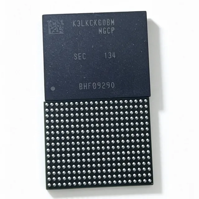
K3LKCKC0BM-MGCP - 64Gb LPDDR5 SDRAM 6400 Mbps | Samsung
The Samsung K3LKCKC0BM-MGCP is a 64 Gbit (8 GB) LPDDR5 SDRAM organized as 2G x32, operating at up to 6400 Mbps pin speed, supplied in a 315-ball FBGA package and rated for -25C to +85C operation. It runs from multiple supply rails including 1.05V, 1.8V, 900mV and 500mV core/interface domains per the LPDDR5 standard. LPDDR5 (Low Power Double Data Rate 5) is a JEDEC-defined CMOS DRAM memory technology optimized for mobile and power-sensitive computing. In the memory hierarchy it sits as the main system DRAM below the CPU/SoC cache, providing high-bandwidth working memory with aggressive power management such as deep power-down, DVFS, and bank group architectures. Key features include 64 Gbit density in a single package, 6400 Mbps data rate (equivalent to 51.2 GB/s aggregate bandwidth in a x32 dual-channel system as promoted on the Samsung LPDDR5 product page), low-voltage signaling for reduced power, and RoHS compliance. The x32 organization supports burst-oriented, channel-interleaved access typical of application processors. Architecturally, the device uses a CMOS DRAM core with LPDDR5 bank-group structure, on-die termination, and speed-grade optioning encoded in the MPN suffix. The MGCP suffix denotes package/speed binning per Samsung ordering information. Typical applications include flagship smartphone main memory, automotive infotainment and ADAS edge-computing SoCs, and AI edge modules where high bandwidth-per-watt is critical. Design consideration: the memory controller and PCB routing must support 6400 Mbps signaling; impedance control, fly-by termination, and per-rail decoupling of the 1.05V/1.8V/900mV/500mV supplies are essential for signal integrity. This page adds value beyond the datasheet by consolidating distributor stock and pricing data, drop-in family alternatives, and practical design notes in one place.
K3LKJKJ0CM-MFCP - 24Gb LPDDR5 DRAM 6400Mbps | Samsung
The Samsung K3LKJKJ0CM-MFCP is a 24 Gbit LPDDR5 (Low Power Double Data Rate 5) SDRAM memory device operating at 6400 Mbps pin speed, supplied in a 315-ball FBGA package with triple-rail power inputs of 1.8V (VDD2), 1.05V (VDD1) and 0.9V (VDDQ). LPDDR5 is the fifth generation of low-power synchronous DRAM defined by JEDEC, positioned within the memory hierarchy as mobile DRAM -> LPDDR family -> SDRAM -> semiconductor memory. It is optimized for battery-powered, thermally constrained systems such as smartphones, tablets, and, in the case of this part number, automotive platforms that require high bandwidth with strict power budgets. Key features of the K3LKJKJ0CM-MFCP include a 24 Gbit (3 GB) die density, a 6400 Mbps data rate (the JEDEC LPDDR5 target speed enabling aggregate transfers up to 51.2 GB/s on 64-bit bus systems), and the triple-supply architecture (1.8V / 1.05V / 0.9V) that separates core and I/O domains for dynamic voltage scaling and power savings of roughly 20% versus LPDDR4X. The 315-ball FBGA (Fine-Pitch Ball Grid Array) package supports high-density surface-mount assembly typical of mobile and automotive memory modules. According to Samsung Semiconductor documentation, LPDDR5 devices of this class add architectural improvements over LPDDR4X, including bank group mode, a replica-based DFE (decision feedback equalization) receiver, and command/address encoding, all of which reduce switching activity and improve signal integrity at 6400 Mbps. Typical applications for this component include automotive ADAS and infotainment memory subsystems, high-performance mobile computing, 5G modems, and edge AI accelerators that require high memory bandwidth in a compact footprint. When designing with this device, verify the exact ball map and speed bin against the official Samsung datasheet for the MFCP package, and pair it with an SoC memory controller that supports the full LPDDR5 protocol, including WCK and DFE training sequences. This page consolidates distributor sourcing data, drop-in alternative options, and practical design notes not found on the manufacturer's product page.
K3LKJKJ0CM-MUCP - 24Gb LPDDR5 DRAM 6400Mbps | Samsung
The Samsung K3LKJKJ0CM-MUCP is a 24 Gbit (3 GB) LPDDR5 SDRAM memory device delivered in a 315-ball FBGA package, supporting data rates up to 6400 Mbps on a multi-rail power architecture of 1.8 V (VDD2), 1.05 V (VDD1) and 0.9 V (VDDQ). LPDDR5 (Low Power Double Data Rate 5) is a JEDEC-defined DRAM interface standard optimized for mobile, automotive and edge-computing platforms. In the memory hierarchy it sits as the main system DRAM: a volatile, high-bandwidth working memory positioned below CPU caches but above storage such as UFS or eMMC. Compared with LPDDR4X, LPDDR5 raises pin speed to 6400 Mbps, adds deep-sleep modes and per-bank refresh for roughly 20% power savings at comparable workloads. Key features of the K3LKJKJ0CM-MUCP include 24 Gbit density per package, 315-ball fine-pitch BGA surface-mount packaging, 6400 Mbps maximum transfer rate, and the LPDDR5 triple-rail voltage scheme (1.8 V / 1.05 V / 0.9 V) that separates core and I/O domains for dynamic power optimization. Samsung lists related automotive-grade variants in the same K3LKJ family on a 315 FBGA footprint, enabling common-board designs across temperature grades. Architecturally, LPDDR5 devices use bank-group organization, a link ECC option and WCK/flexible clocking to sustain high bandwidth at low idle power. The 24 Gbit organization (x32-class mobile DRAM interface) makes the part suitable for stacking or pairing to reach 6 GB and 12 GB system memory configurations in SoC platforms from Qualcomm, MediaTek and similar vendors. Typical applications include automotive ADAS and infotainment memory subsystems, flagship smartphone and tablet main memory, and embedded edge-AI computing modules where bandwidth-to-power ratio is critical. A key design consideration is power integrity: the separated 0.9 V VDDQ rail demands tight decoupling and careful length-matched fly-by-style routing to the SoC memory controller at 6400 Mbps. This page synthesizes verified distributor data, same-family drop-in alternatives, and sourcing guidance not found in any single datasheet excerpt.

K4A4G045WD-BCRC - 4Gb DDR4 SDRAM x4, 1.2V | Samsung
The Samsung K4A4G045WD-BCRC is a 4Gb DDR4 SDRAM component organized as 1G x4, operating at 1.2V VDD in a 78-ball TFBGA (FBGA-78) package. The BCRC speed bin supports 2400 Mbps data rates per the Samsung D-die DDR4 product selection guide. DDR4 SDRAM (Double Data Rate 4 Synchronous Dynamic Random Access Memory) is the fourth generation of the DDR DRAM family, defined by JEDEC as the successor to DDR3. In the memory hierarchy, this device is a DRAM component (not a module) that sits beneath memory modules and above NAND storage, providing volatile, high-speed working memory for processors and SoCs. DDR4 lowers the core operating voltage to 1.2V versus 1.5V for DDR3, increases bank counts, and adds features such as bank groups and a 2n refresh architecture for 8Gb-class devices. Key features of the K4A4G045WD include 4Gb density on Samsung's D-die process, a x4 organization suited to error-correcting-code (ECC) memory subsystems where check bits run on dedicated data lanes, and a 78-ball fine-pitch BGA footprint that supports high-density memory arrays. DDR4's 8-bank group structure (four groups of four banks) with tCCD_S/tCCD_L timings enables higher effective bandwidth than DDR3 at the same clock. Technically, the device uses a double-data-rate command/address interface and on-die termination (ODT) to maintain signal integrity at 2400 Mbps transfer rates. A differential clock pair (CK/CK#) and strobes (DQS/DQS#) window data capture, while a reset pin (RESET#) allows low standby power. As an ECC-friendly x4 device, it is typically paired with memory controllers supporting SECDED error correction for industrial and server-class reliability. Typical applications include embedded and industrial motherboards, networking line cards, storage controllers, and server DIMMs where long-term component availability matters. Samsung positions this DDR4 lineup for embedded, industrial, and server-grade memory applications as the industry migrates toward DDR5. Design consideration: DDR4 routing requires length-matched fly-by command/address topology, per-byte termination, and careful VREF training; consult the memory controller's DDR4 design guide before layout. This page synthesizes distributor stock data, drop-in alternatives, and practical design notes not found in the manufacturer datasheet alone. Pricing is quote-based as of 2026-09-04.
K4A4G085WD-BCPB - 4Gb DDR4 SDRAM x8 1.2V | Samsung
The Samsung K4A4G085WD-BCPB is a 4Gb (512M x 8) DDR4 SDRAM fabricated on Samsung's D-die process node, operating from a 1.2V supply in a 78-ball FBGA (PB lead-free halogen-free) package. According to Samsung's K4A4G085WD datasheet, the device is a fourth-generation DDR4 SDRAM component intended for memory modules and embedded systems. A DDR4 SDRAM (Double Data Rate 4 Synchronous Dynamic Random Access Memory) is a type of volatile memory IC that transfers data on both clock edges, sitting within the memory hierarchy as DRAM -> synchronous DRAM -> DDR SDRAM -> DDR4 SDRAM. DDR4 lowered operating voltage from 1.5V (DDR3) to 1.2V and increased bank-group architecture, improving bandwidth and power efficiency in servers, desktops, and industrial controllers. Key features of this component include its 4Gb density in a x8 organization, 1.2V core supply consistent with the DDR4 JEDEC-era interface used across the industry, and the compact FBGA-78 footprint that enables high-density module layouts. The D-die generation provides the electrical characteristics Samsung documented in the K4A4G085WD family datasheet. Architecturally, the device uses Samsung's D-die process with DDR4 bank-group parallelism, burst-oriented operation, and on-die termination practices typical of the DDR4 generation. Timing and AC parameters must be taken from the official Samsung K4A4G085WD datasheet for the specific speed grade. Typical applications include UDIMM/SODIMM/RDIMM memory modules, embedded systems, industrial PCs, networking equipment, and set-top platforms that use discrete DDR4 components with a x8 data width. When designing with this part, follow Samsung's DDR4 routing guidelines for fly-by or tree topology, length-matched address/command lines, and proper VTT/VDDQ decoupling; confirm the exact speed grade and timing parameters from the datasheet for your controller. This page synthesizes verified distributor listings, drop-in alternatives, and sourcing context not found in the manufacturer datasheet, helping engineers and buyers evaluate the K4A4G085WD-BCPB alongside pin-compatible DDR4 options.
K4A4G085WD-BCTD - 4Gb DDR4 SDRAM 512Mx8 2666Mbps | Samsung
The Samsung K4A4G085WD-BCTD is a 4Gb DDR4 SDRAM organized as 512M x 8, operating at up to 2666 Mbps data rate from a 1.2V supply in a 78-ball FBGA package with a 0-85C commercial operating temperature range. It belongs to Samsung's D-die DDR4 generation. DDR4 SDRAM (Double Data Rate fourth-generation synchronous dynamic random access memory) is the dominant main-memory technology in computing systems. As a volatile memory IC within the DRAM -> SDRAM -> DDR SDRAM -> DDR4 hierarchy, it stores data in capacitor-based cells refreshed by the memory controller, offering far higher density and lower power per bit than DDR3 while adding bank groups, DBI, and CA parity. Key features include 4Gb (512 Meg x 8) density, a 2666 Mbps/pin data rate (PC4-21300 class), 1.2V core supply that cuts power roughly 20% versus DDR3's 1.5V, and the space-saving 78-ball FBGA (0.8 mm ball pitch) surface-mount package. The D-die silicon uses Samsung's advanced DRAM process node to achieve the DDR4-2666 speed bin with standard JEDEC DDR4 command timing. Internally the device is structured with bank groups enabling faster back-to-back access, and it supports standard DDR4 features such as burst chop, on-die termination (ODT), and DLL for reliable high-speed signaling. Typical applications include main memory for embedded x86/ARM processors, industrial controllers, networking equipment, set-top boxes, and computing modules where a single 4Gb x8 DRAM provides a cost-effective 512 MB memory footprint. Design consideration: DDR4-2666 routing requires careful length matching and ODT calibration; confirm your memory controller supports the D-die speed bin and set the MR (mode register) configuration per the Samsung datasheet. This page adds value beyond the datasheet by consolidating verified specs, drop-in alternatives from Samsung, Micron and the F-die family, and practical design guidance for BOM migration.