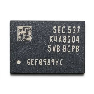
K4A4G085WD-BCTD - 4Gb DDR4 SDRAM 512Mx8 2666Mbps | Samsung
MPN: K4A4G085WD-BCTD ✓ Active| Qty | Unit Price | Extended |
|---|---|---|
| 1 | $2.85 | $2.85 |
| 10 | $2.62 | $26.20 |
| 100 | $2.4 | $240.00 |
| 500 | $2.21 | $1,105.00 |
| 1,000 | $2.05 | $2,050.00 |
K4A4G085WD-BCTD Overview
DDR4 SDRAM (Double Data Rate fourth-generation synchronous dynamic random access memory) is the dominant main-memory technology in computing systems. As a volatile memory IC within the DRAM -> SDRAM -> DDR SDRAM -> DDR4 hierarchy, it stores data in capacitor-based cells refreshed by the memory controller, offering far higher density and lower power per bit than DDR3 while adding bank groups, DBI, and CA parity.
Key features include 4Gb (512 Meg x 8) density, a 2666 Mbps/pin data rate (PC4-21300 class), 1.2V core supply that cuts power roughly 20% versus DDR3's 1.5V, and the space-saving 78-ball FBGA (0.8 mm ball pitch) surface-mount package.
The D-die silicon uses Samsung's advanced DRAM process node to achieve the DDR4-2666 speed bin with standard JEDEC DDR4 command timing. Internally the device is structured with bank groups enabling faster back-to-back access, and it supports standard DDR4 features such as burst chop, on-die termination (ODT), and DLL for reliable high-speed signaling.
Typical applications include main memory for embedded x86/ARM processors, industrial controllers, networking equipment, set-top boxes, and computing modules where a single 4Gb x8 DRAM provides a cost-effective 512 MB memory footprint.
Design consideration: DDR4-2666 routing requires careful length matching and ODT calibration; confirm your memory controller supports the D-die speed bin and set the MR (mode register) configuration per the Samsung datasheet.
This page adds value beyond the datasheet by consolidating verified specs, drop-in alternatives from Samsung, Micron and the F-die family, and practical design guidance for BOM migration.
Drop-in alternatives for K4A4G085WD-BCTD — same package, pin-to-pin compatible. Different-package parts requiring PCB rework are excluded.
Variants in this series
Same-series models that are drop-in compatible with K4A4G085WD-BCTD (same form factor and footprint) — differing in Package, Data Rate, Interface, Memory Type, Mounting Type.
Quick Comparison Tool — Select alternative parts for side-by-side comparison:
K4A4G085WD-BCRC
✅ Drop-In✓ In Stock
$3.58 / Unit
View Datasheet →K4A4G085WD-BCPB
✅ Drop-In✓ In Stock
Contact for price
View Datasheet →K4A4G085WE-BCTD
✅ Drop-In📋 Reference alternative (not in catalog)
K4A4G085WF-BCTD
✅ Drop-In📋 Reference alternative (not in catalog)
MT40A512M8RH-075E:B
✅ Drop-In✓ In Stock
$2.15 / Unit
View Datasheet →K4A4G085WD-BCTD Maximum Ratings & Electrical Characteristics
| Memory Type | DDR4 SDRAM |
| Die Generation | D-die |
| Density | 4 Gb |
| Organization | 512M x 8 |
| Data Rate | 2666 Mbps/pin |
| Supply Voltage | 1.2 V |
| Operating Temperature | 0C to +85C |
| Package | 78-ball FBGA |
| Ball Pitch | 0.8 mm |
| Mounting Type | Surface Mount |
| Interface | DDR4 (JEDEC-compatible) |
| Speed Class | DDR4-2666 (PC4-21300) |
| Bank Architecture | DDR4 bank-group architecture |
| On-Die Termination (ODT) | Yes |
| DLL | Yes |
K4A4G085WD-BCTD 78-ball fbga Pin Configuration Guide
Pin configuration for K4A4G085WD-BCTD (78-ball fbga package). This digital IC includes GPIO, communication interfaces (UART, SPI, I2C), and power pins. Refer to the manufacturer datasheet for alternate pin functions and configuration options. Essential for embedded system design and PCB layout.

No detailed pinout data available for K4A4G085WD-BCTD.
Refer to the datasheet for full pin configuration.
Typical Applications
K4A4G085WD-BCTD is suitable for 6 applications: Embedded Main Memory for Industrial Controllers, Networking and Communication Equipment, Set-Top Boxes and Smart TV Platforms, Computing Modules (SODIMM/COM Express), Data Logging and Edge IoT Gateways, Test and Measurement Instrumentation.
Embedded Main Memory for Industrial Controllers
The K4A4G085WD-BCTD provides 512 MB of DDR4-2666 main memory (512M x 8, 1.2V) for industrial PCs, PLCs, and edge controllers built on embedded x86 or ARM SoCs with DDR4 controllers. Its 2666 Mbps data rate supplies roughly 2.6 GB/s of peak bandwidth per x8 channel, sufficient for real-time control loops, protocol stacks, and local data buffering. The 0-85C commercial rating covers most cabinet-based industrial environments, and the 78-ball FBGA's 0.8 mm pitch suits standard 4-layer routing. Placed on a short (~40 mm) address/command bus with on-die termination enabled, the device trains reliably at DDR4-2666 with standard ODT settings; for longer or multi-drop buses, reduce speed by one bin to preserve margin.
Recommended
Networking and Communication Equipment
Switches, routers, and GPON/5G small-cell equipment use a single K4A4G085WD-BCTD per control-plane CPU to hold packet buffers, routing tables, and firmware working sets. The DDR4-2666 speed class and bank-group architecture deliver the low-latency random access that table lookups demand, while 1.2V operation keeps the per-DIMM-slot power budget low in fanless designs. The 4Gb x8 organization maps cleanly to 32-bit and 64-bit memory controllers using two or eight devices. Because network gear runs 24/7, designers should derate the junction temperature, use 1% VTT termination regulation, and re-run memory training after any die-generation substitution (D-die to F-die) to preserve bit-error-rate margins.
Recommended
Set-Top Boxes and Smart TV Platforms
Consumer AV platforms pair the K4A4G085WD-BCTD with SoCs that stream, decode, and buffer 4K video. The 512 MB x8 footprint covers OS, middleware, and frame buffers for HD-class products, and DDR4-2666 bandwidth sustains concurrent decode/display paths. The 1.2V supply and D-die process reduce standby power, which matters for always-on listening modes mandated in set-top boxes. The 78-ball FBGA fits the dense, cost-optimized two-layer-memory layouts typical of consumer boards. Thermal design is straightforward at single-device populations, but board designers must keep the clock and DQS lines length-matched to datasheet skew limits to avoid intermittent training failures across production variability.
Recommended
Computing Modules (SODIMM/COM Express)
Computer-on-modules and memory daughtercards populate multiple K4A4G085WD-BCTD devices to build 1-4 GB DDR4-2666 arrays on a 64-bit bus. The uniform 78-ball x8 FBGA footprint lets one PCB land pattern serve Samsung D/E/F-die and Micron equivalents, giving module makers BOM flexibility during DRAM allocation cycles. DDR4's bank groups and DBI support help modules meet signal-integrity targets at 2666 Mbps on 8-10 layer stackups. Module vendors should store die-generation and speed-bin data in the SPD EEPROM, re-characterize write leveling per die swap, and validate the full population across the 0-85C range with margin testing before release to production.
Recommended
Data Logging and Edge IoT Gateways
Edge gateways that aggregate sensor streams, run containers, and buffer uploads to the cloud benefit from the K4A4G085WD-BCTD's 512 MB working memory at 1.2 V. DDR4-2666 bandwidth handles concurrent write-ahead logging and TLS sessions, while the D-die's low refresh overhead keeps idle power low for battery-backed nodes. The x8 organization suits single-device, 32-bit controller designs common in gateway SoCs. Designers should ensure the power-good sequencing of the 1.2V and VTT rails follows the SoC vendor's DDR4 power-up procedure, and should reserve PCB escape routing compatible with F-die parts so that a future substitution to K4A4G085WF-BCTD requires no layout revision.
Recommended
Test and Measurement Instrumentation
Oscilloscopes, logic analyzers, and signal generators use DDR4 SDRAM for deep waveform capture memory. The K4A4G085WD-BCTD's 2.6 GB/s peak bandwidth and 512M x8 organization provide cost-effective capture depth when multiplied across channels, and DDR4's burst-chop mode supports the mixed sequential/random access patterns of acquisition engines. Because instruments demand sustained error-free operation, designs should enable CA parity if the controller supports it, implement robust training across temperature, and validate RAS/CAS timing at the DDR4-2666 corner per the Samsung datasheet. The 78-ball FBGA reflows onto standard instrumentation PCBs without special thermal features at single-device loads.
Recommended
Recommended Products Summary
Engineering reference data for K4A4G085WD-BCTD — comparison, design guidance, and compliance information.
Selection Guide
Comparison with Alternatives
| Parameter | This Product | K4A4G085WD-BCRC | K4A4G085WF-BCTD | MT40A512M8RH-075E:B |
|---|---|---|---|---|
| Package | 78-ball FBGA | 78-ball FBGA - same | 78-ball FBGA - same | 78-ball FBGA - same |
| Brand | Samsung Electronics | Samsung Electronics | Samsung Electronics | Micron Technology |
| Density | 4 Gb | 4 Gb | 4 Gb | 4 Gb |
| Organization | 512M x 8 | 512M x 8 | 512M x 8 | 512M x 8 |
| Supply Voltage | 1.2 V | 1.2 V | 1.2 V | 1.2 V |
| Die Generation | D-die | D-die | F-die | Micron B-die (E:suffix rev) |
Key Differentiators
- D-die maturity with proven controller support (vs K4A4G085WF-BCTD)
- Cost-efficient x8 organization (vs K4A4G165WF-BCTD (x16 sibling))
- Identical footprint to Micron equivalent for dual-sourcing (vs MT40A512M8RH-075E:B)
Design Notes
At DDR4-2666, keep address/command trace skew within the controller's datasheet window (typically +/-25 ps on short point-to-point buses) and length-match DQ/DM/DQS per byte lane to within 25 mils. Enable on-die termination (ODT) on both writes and reads and tune RZQ settings during memory training rather than hard-coding values; D-die training tables differ from F-die, so retrain after any die substitution. Route the 1.2V rail as a plane, not a trace, to minimize di/dt droop during simultaneous switching.
Estimated: a single 4Gb DDR4 device at DDR4-2666 typically draws 300-500 mA average from the 1.2V rail at full utilization (per JEDEC-style current estimates in the Samsung datasheet); size the point-of-load converter for at least 0.8 A headroom and add bulk capacitance (e.g., 47 uF) plus 0.1 uF ceramics at each ball group. Sequence VDD before/with VTT per the SoC vendor's power-up procedure - violating DDR4 power sequencing is a common cause of training failure and latent device stress.
Do not assume all 4Gb x8 DDR4 parts are interchangeable: D-die (WD), E-die (WE) and F-die (WF) differ in training margins and lifecycle status, and some controller compatibility lists restrict die generations. Confirm the temperature suffix - BCTD is 0-85C commercial and is NOT qualified for -40C industrial ambient. Finally, remember the 8Gb K4A8G085W parts use a different ball count and are not drop-in compatible despite similar naming.
Compliance Information
Compliance data was not present in the retrieved web data; obtain RoHS/REACH declarations from Samsung's environmental reporting portal. Samsung DRAM of this generation is typically lead-free and halogen-free, but this must not be assumed without documentation.