Memory ICs
Subcategories
Products (476)
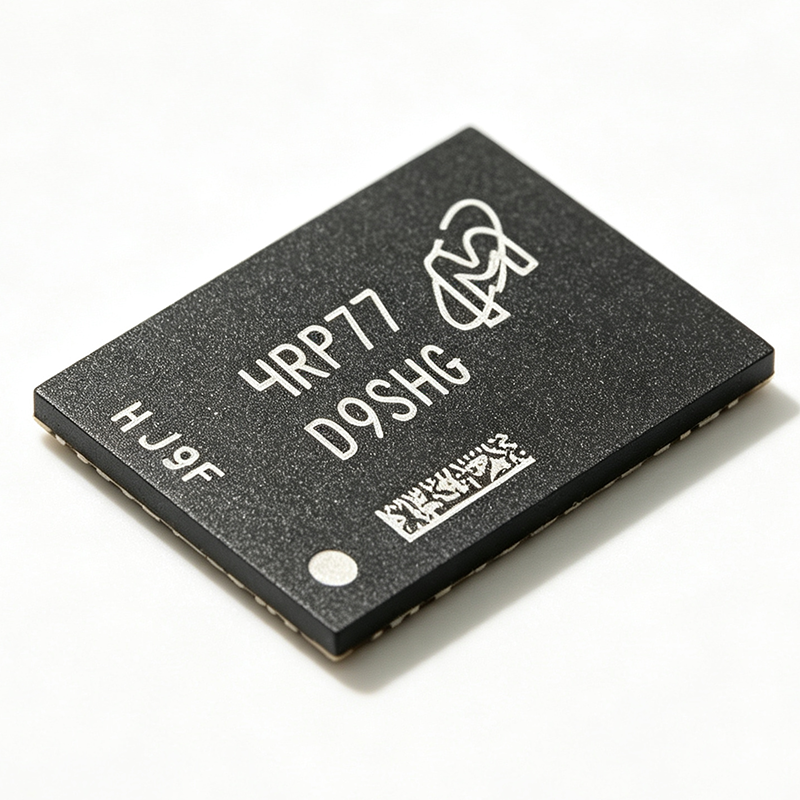
MT41K256M16TW-107IT - 4Gb DDR3L SDRAM 933MHz | Micron
The Micron MT41K256M16TW-107IT is a 4Gb DDR3L SDRAM organized as 256M x 16, operating at 1.35V with a data rate of 933 MHz (DDR3L-1866). It comes in a 96-ball FBGA (8x14mm) package and is designed for industrial temperature range (-40°C to +95°C). This memory IC is widely used in networking, embedded computing, and industrial applications where high density and low power are critical. DDR3L (Double Data Rate 3 Low Voltage) is a type of synchronous dynamic random-access memory (SDRAM) that operates at 1.35V, reducing power consumption by about 20% compared to standard 1.5V DDR3. It is part of the DDR3 family, which uses double data rate signaling to transfer data on both edges of the clock, achieving high bandwidth. DDR3L is backward compatible with DDR3 slots in many systems, making it a popular choice for upgrades and new designs. Key features include a parallel interface with 16-bit data bus, 20ns access time, and support for auto self-refresh, auto precharge, asynchronous reset, output enable, dynamic on-chip termination (ODT), ZQ calibration, and write leveling. These features enhance signal integrity and simplify system design. The industrial temperature range ensures reliable operation in harsh environments. The MT41K256M16TW-107IT uses Micron's advanced CMOS process technology, offering high density and low power. The 96-ball FBGA package provides excellent thermal and electrical performance, with a compact footprint suitable for space-constrained designs. The device supports JEDEC-standard DDR3L timing, ensuring compatibility with a wide range of controllers. Typical applications include networking equipment (routers, switches), embedded systems, industrial PCs, and test and measurement instruments. Its high density and low voltage make it ideal for memory-intensive applications where power efficiency is important. When designing with this device, ensure proper decoupling and follow the layout guidelines in the datasheet to maintain signal integrity at 933 MHz. The industrial temperature grade requires adequate thermal management to keep the junction temperature within specified limits.
MT42L64M32D2HE-18 - 2Gbit LPDDR2 SDRAM 533MHz | Micron
The Micron Technology MT42L64M32D2HE-18 is a 2 Gbit Mobile Low-Power DDR2 (LPDDR2) SDRAM memory IC organized as 64M x 32 bits, operating at a maximum clock frequency of 533 MHz, housed in a 134-ball VFBGA package measuring 10 x 11.5 mm. LPDDR2 SDRAM is a class of DRAM optimized for low power consumption in battery-operated and thermally constrained systems. Unlike standard DDR SDRAM, LPDDR2 uses a 1.2V core supply, operates at lower voltages on its I/O, and supports power-down, self-refresh, and deep-power-down modes that dramatically reduce standby current. Within the memory hierarchy, LPDDR2 sits between the older LPDDR (LPDDR1) and the newer LPDDR3/LPDDR4 standards, offering a fly-by-free parallel interface with CA pin command/address multiplexing. Key features of this device include the 2 Gbit density in a single 64M x 32 organization, 533 MHz operation (LPDDR2-S4 class), industrial temperature rating of -40C to +85C for the IT:D variant, and the compact 134-VFBGA (10 x 11.5 mm) package that conserves board area in space-limited designs. The D suffix in the part number denotes die revision and a lead-free/RoHS-compliant package. Architecturally, the MT42L64M32D2HE implements multiple internal banks with burst access, supporting both non-multiplexed and multiplexed addressing. The x32 I/O organization reduces bus turnaround latency compared with narrower organizations, improving effective bandwidth in real-time embedded workloads. Low-voltage signaling lowers I/O switching power, which is critical for handheld and connected devices. Typical applications include portable media players, tablet and e-reader main memory, networking and communication equipment buffers, industrial human-machine interfaces, and automotive infotainment (using the AAT:D/AUT:D temperature variants of the same die). Design consideration: LPDDR2 requires careful PCB length matching on the CA, DQ, and DQS signal groups, plus regulated 1.2V core and VDDQ rails; consult the Micron LPDDR2 datasheet for tCK tolerances and ZQ calibration requirements before layout. This page synthesizes distributor pricing, drop-in same-family alternatives, and practical design notes not found in the manufacturer datasheet alone.
MT53B128M32D1NP-062 - 4Gbit LPDDR4 SDRAM 1.6GHz | Micron
The Micron Technology MT53B128M32D1NP-062 is a 4 Gbit Mobile LPDDR4 SDRAM organized as 128M x 32, operating at a 1.6 GHz clock frequency from a 1.1V supply, housed in a 200-ball WFBGA (10 x 14.5 mm) package. LPDDR4 (Low Power Double Data Rate 4) SDRAM is a member of the JEDEC-defined DDR SDRAM family optimized for mobile and power-sensitive embedded systems. Compared with DDR3L or DDR4, LPDDR4 achieves higher bandwidth per watt by lowering the core supply voltage to 1.1V and using a point-to-point channel architecture. In the memory hierarchy it sits under DRAM -> synchronous DRAM -> mobile SDRAM, and it is the dominant main-memory technology in smartphones, tablets, automotive infotainment, and edge AI platforms. Key features of this device include 4 Gbit density in a single 32-bit channel organization (128M x 32), 1.6 GHz operation (3200 MT/s data rate class), a low 1.1V core supply, and extended industrial or automotive temperature variants (the AUT:A grade is specified from -40C to +125C TC and qualified to AEC-Q100). The -062 speed grade defines the maximum clock frequency of the part. The WFBGA package uses a ball grid array for improved signal integrity and thermal performance relative to wire-bonded alternatives. Technically, the MT53B128M32D1NP family integrates Micron's LPDDR4 core with bank-group architecture, enabling fast random row access and efficient burst interleaving. Low-power features such as partial-array self-refresh, deep power-down, and per-bank refresh reduce standby current, which directly extends battery life in portable designs. The 32-bit single-die organization simplifies controller mapping for mid-density systems that do not require a full 64-bit dual-die configuration. Typical applications include automotive infotainment and instrument cluster memory, industrial human-machine interfaces, edge AI accelerators, networking line cards, and embedded vision systems where 4 Gbit of bandwidth-efficient DRAM is sufficient. When designing with this device, ensure your memory controller supports the JEDEC LPDDR4 protocol, and account for trace-length matching and termination on the high-speed data bus to meet signal-integrity requirements at 1.6 GHz operation. This page synthesizes distributor pricing, drop-in alternatives, and practical design notes not found in the manufacturer datasheet, with data verified as of 2026-09-02.
MT53D512M32D2NP-046 - 16Gbit LPDDR4 2133MHz DRAM | Micron
The Micron Technology MT53D512M32D2NP-046 is a 16Gbit Mobile LPDDR4 SDRAM memory IC organized as 512M x 32, operating at a 2.133 GHz data rate from a 1.1V core supply, housed in a 200-ball WFBGA package measuring 10 mm x 14.5 mm. LPDDR4 (Low Power Double Data Rate 4) is a JEDEC-defined class of DRAM optimized for mobile and power-sensitive embedded systems. Within the memory hierarchy, it sits below DDR4 server DIMMs in density per channel but far above them in power efficiency, using a low-voltage interface, deep power-down modes, and per-bank refresh to minimize energy per bit transferred. Key features include the high 16Gbit density in a single package, a 32-bit wide data bus that simplifies controller interfaces for application processors, and the -046 speed grade supporting 2133 MHz operation. Micron's D2NP NP (non-stack, single-die-planar) configuration offers a straightforward signal integrity profile compared with multi-die stacked alternatives. Architecturally, the device uses a standard LPDDR4 core with bank groups, burst length 8 and 16 access modes, and dynamic frequency scaling that lets the host processor reduce the clock in idle periods to cut quiescent power. The 1.1V VDD rail, combined with separate VDDQ I/O domain, allows fine-grained power management in battery-driven designs. Typical applications include mobile smartphone and tablet main memory, automotive infotainment and ADAS platforms (using the AIT/AUT automotive-grade variants), networking appliances, and industrial embedded computing where a compact footprint and low standby current matter. When designing with this device, pay careful attention to the 200-WFBGA fly-by routing topology, length-matched address/command lines, and reference voltage (VREFCA/VREFDQ) decoupling, as LPDDR4 timing budgets are tighter than DDR3L predecessors. On-die termination (ODT) settings should be validated across the full temperature range. This page synthesizes distributor pricing and availability, same-package drop-in alternatives including the MT53E LPDDR4X successor, and practical layout guidance not found in the manufacturer datasheet.
MT53E2G32D4DE-046 - 64Gbit LPDDR4X SDRAM 2133MHz | Micron
The Micron Technology MT53E2G32D4DE-046 is a 64Gbit mobile LPDDR4X SDRAM organized as 2G x 32, operating at 2133 MHz (3.5 ns cycle) in a 200-ball TFBGA package measuring 10 x 14.5 mm. As an LPDDR4X device, it uses low-VDDQ I/O (1.06 V to 1.17 V supply) to cut interface power versus standard LPDDR4. LPDDR4X (Low Power Double Data Rate 4X) is a JEDEC-defined mobile DRAM interface optimized for battery-powered and bandwidth-hungry systems. In the memory hierarchy it sits as high-density, high-speed working memory: DRAM -> synchronous DRAM -> mobile LPDRAM -> LPDDR4X, providing the main volatile working storage between the application processor and nonvolatile flash storage. Key features include the 64Gbit density in a single die, x32 I/O width, 2133 Mbps data rate per pin, auto precharge, write leveling, ZQ calibration, a built-in temperature sensor, auto self-refresh, data mask (DM) function, and an asynchronous reset input. The temperature sensor enables autonomous self-refresh rate adjustment, protecting data retention while minimizing refresh power across the operating range. Technically, the device is a high-speed CMOS dynamic random-access memory with a 16n-bank architecture and quarter-density bank grouping, transferring on both clock edges at 2.133 GHz effective. The -046 speed bin defines the 3.5 ns clock cycle. Available temperature grades include WT (-25C to +85C), AIT (-40C to +95C, industrial), and AUT (-40C to +125C, automotive), all sharing the same die and 200-ball footprint. Typical applications include AI edge accelerators, NVIDIA Jetson-class modules, automotive infotainment and ADAS domains, 5G network equipment, and industrial HMI systems requiring 8GB-class DRAM with LPDDR4X power efficiency. Design consideration: LPDDR4X fly-by routing requires per-byte write leveling and careful length matching; verify VDD2/VDDQ rail sequencing per the manufacturer datasheet power-up procedure to avoid latch-up. This page synthesizes distributor pricing, temperature-grade alternatives, cross-reference guidance, and practical design notes not consolidated in the manufacturer datasheet.
MT53E768M64D4HJ-046 - 48Gbit LPDDR4X SDRAM | Micron
The Micron Technology MT53E768M64D4HJ-046 is a 48Gbit Mobile LPDDR4X SDRAM memory IC organized as 768M x 64, operating at 2133 MHz (2133 Mbps/pin data rate, 3.5 ns access time) with an LVSTL I/O interface, housed in a 556-ball WFBGA (12.4 mm x 12.4 mm) package. LPDDR4X (Low Power Double Data Rate 4X) is a JEDEC-defined high-bandwidth, low-voltage mobile DRAM standard used as the main-system memory in smartphones, tablets, automotive infotainment, and edge-AI compute platforms. LPDDR4X sits within the mobile DRAM hierarchy alongside LPDDR4 and below LPDDR5, and is distinguished from LPDDR4 by a lower VDDQ I/O supply that significantly reduces interface power at the same data rate. Key features of this device include its 48Gbit (6 GB) density in a single package, a wide 64-bit data bus, 2133 MHz clock rate with 3.5 ns access latency, and the ultra-compact 556-ball fine-pitch BGA (FBGA/WFBGA) footprint suited to space-constrained PCBs. Micron offers this die in multiple temperature and status suffixes (AAT, AUT, AIT, WT) covering commercial and automotive-grade operating conditions. The MT53E LPDDR4X family uses a CMOS dynamic memory core with bank-group architecture supporting burst accesses over a parallel interface, and quad-die package (QDP) variants are referenced by distributors (FBGA QDP coding on the B-suffix speed bins). Signals use LVSTL (Low Voltage Swing Terminated Logic) terminated I/O for signal integrity at 2133 Mbps/pin. Typical applications include automotive digital cockpits and ADAS platforms, high-resolution mobile displays and handsets, networking and edge-AI compute modules, and embedded systems requiring multi-gigabyte memory bandwidth in a small footprint. Design consideration: LPDDR4X routing demands strict length matching of the 64-bit data bus, on-die-termination configuration during controller initialization, and a regulated VDD2/VDDCA power rail with fast transient response; consult the Micron datasheet and controller compatibility list before layout. This page synthesizes distributor listings, temperature-suffix variants, and drop-in same-die alternatives not consolidated in the manufacturer part catalog.
MT58L64L32FT-10 - 2Mb Sync Burst SRAM 10ns 66MHz | Micron
The Micron Technology MT58L64L32FT-10 is a 2-Mbit flow-through synchronous burst SRAM organized as 64K x 32/36 (also configurable as 128K x 18), delivering a fast 10 ns clock/access time at clock rates up to 66 MHz in a 100-lead TQFP (14 x 20.1 mm) package. A synchronous burst SRAM is a static random-access memory that synchronizes address, data, and control inputs to an external clock and generates burst addresses internally, making it a key member of the memory IC family that sits within the broader semiconductor hierarchy (SRAM -> static RAM -> volatile memory -> memory IC -> integrated circuit). Unlike asynchronous SRAMs, burst-mode devices such as the MT58L64L32FT-10 prefetch sequential addresses, reducing effective access time for cache-like workloads and pipelined bus masters. Key features include single +3.3 V power supply (VDD, +0.3 V/-0.165 V tolerance), a separate isolated +2.5 V or 3.3 V output buffer supply (VDDQ) for I/O voltage flexibility, fast clock-to-output and OE# access times, individual BYTE WRITE enable controls, and SNOOZE MODE for reduced-power standby. Common data input/output pins simplify bus routing on 32-bit and 36-bit (byte-parity) systems. Architecturally, the flow-through (non-pipelined) SyncBurst design presents data on the same cycle the address is captured, eliminating pipeline latency and simplifying timing closure for controllers that expect zero-wait-state reads and writes. Registered outputs driven by the internal burst address counter support linear, interleaved, and alternate burst sequences per industry-standard processor burst orders. Typical applications include network router and switch line-card buffering, FPGA and DSP external memory expansion, telecom equipment control-plane memory, industrial controllers, and test instrumentation where deterministic 10 ns access and 66 MHz burst throughput are required. Design considerations: tie VDDQ to the host bus I/O voltage (2.5 V or 3.3 V), use SNOOZE MODE (asserting ZZ) to cut standby power during idle periods, and verify burst-order configuration straps against the host processor (linear vs. interleaved) before layout freeze. This page synthesizes distributor availability data, same-family drop-in speed/temperature variants, and practical design guidance not consolidated in the manufacturer datasheet.
MT62F1536M32D4DS-023 - 48Gbit LPDDR5X SDRAM | Micron Technology
The Micron Technology MT62F1536M32D4DS-023 is a 48Gbit Mobile LPDDR5X SDRAM memory IC organized as 1.5G x 32, operating at up to 4.266 GHz with LVSTL (Low Voltage Swing Terminated Logic) interface signaling, supplied in a 315-ball TFBGA (12.4 mm x 15 mm) surface-mount package. LPDDR5X (Low Power Double Data Rate 5X) is the extended-speed evolution of the LPDDR5 DRAM standard defined by JEDEC, engineered for mobile and power-constrained computing. As a volatile SDRAM within the broader memory hierarchy (DRAM -> mobile DRAM -> LPDRAM), it stores working data for application processors while minimizing power per bit transferred, making it the dominant main-memory technology in smartphones, tablets, and AI edge devices. Key features of this component include the 48 Gbit (6 GB) density in a single package, the 1.5G x 32 organization that supports wide 32-bit memory channels, and the LPDDR5X speed grade supporting a 4.266 GHz clock rate - a substantial bandwidth uplift over LPDDR5 (3.2 GHz, as seen in the related WT:B variant). The LVSTL interface reduces I/O swing to lower simultaneous-switching noise and I/O power at multi-gigahertz data rates. The device operates from a supply voltage of 1.01 V to 1.12 V (VDDQ domain), reflecting the reduced core and I/O voltages that define the LPDDR5X generation. The 315-TFBGA package (12.4 x 15 mm) uses a fine-pitch ball grid array to accommodate the high ball count required by the 32-bit data bus, address/control, and power delivery - a footprint intended for HDI (high-density interconnect) mobile-class PCB stackups. Typical applications include flagship smartphone main memory, AI accelerator and edge-inference modules that stream large weight arrays, automotive infotainment and ADAS domains (the AEC-Q100-qualified AUT:C variant of this same die serves that market), and high-performance portable compute such as tablets and XR headsets. High bandwidth at low power per gigabyte is the common requirement across all of these. Design consideration: LPDDR5X signal integrity demands strict length matching of the data groups, careful controller training for read/write eye margins, and following the power-rail sequencing and termination guidance in the manufacturer datasheet; reuse a validated reference layout rather than improvising the fly-by topology. This page synthesizes distributor pricing and availability, drop-in same-die variant comparisons (WT, AUT, AAT, AIT speed/temperature options), and practical design notes not found in the manufacturer datasheet.

N25Q016A11EV7A0 - 16Mbit SPI NOR Flash 108MHz | Micron
The Micron Technology N25Q016A11EV7A0 is a 16Mbit (2 MB) SPI NOR flash memory device operating from a 1.8V supply with a maximum SPI clock frequency of 108 MHz, housed in an 8-pin WSON (DFN-8 style) surface-mount package. It is a member of Micron's N25Q embedded flash family, which executes code-in-place (XIP) with a single data line and supports standard, dual, and quad SPI protocols. SPI NOR flash is a type of non-volatile memory organized as a serial-access memory array addressed through the Serial Peripheral Interface. Within the memory hierarchy, it sits in the code-storage class (NOR allows random read access for direct code execution), as opposed to NAND flash used for bulk data storage. NOR flash is the standard boot memory for embedded processors, microcontrollers, FPGAs, and system BIOS storage. Key features of the N25Q016A11EV7A0 include the 108 MHz maximum clock rate (the highest speed grade of the N25Q 16Mbit class), 1.8V core supply typical of battery-powered and portable designs, and sector/block-based erasure with page programming. The device supports fast read, dual output read, and quad I/O commands that reduce effective boot time in embedded systems. Architecturally, the 16 Mbit array is organized into uniform sectors with an SPI command set compatible with the broad N25Q/M29P family, easing migration across density points. The V11 suffix denotes the 1.8V supply class; the EV suffix denotes the 8-pin WSON package; the A0 grade denotes the standard industrial part. Typical applications include FPGA configuration storage, MCU code and data storage in industrial controls, networking equipment boot ROM, automotive infotainment subsystems where non-automotive grade is acceptable, and consumer electronics firmware storage. Design consideration: place a 100 nF ceramic decoupling capacitor as close as possible to the VCC pin, and keep SPI clock traces short with a series termination resistor on SCK at 108 MHz operation. This page synthesizes distributor pricing, stock availability, and drop-in alternative analysis not consolidated in the manufacturer datasheet.
N25Q032A13ESFA0F - 32Mb, 3V, 108MHz SPI NOR Flash | Micron
The Micron Technology N25Q032A13ESFA0F is a 32Mb (4MB) 3V multiple I/O serial NOR flash memory with a 108 MHz SPI-compatible clock interface, supplied in a 16-pin wide SOIC package on tape and reel. It is fabricated on Micron's 65nm NOR process technology and is positioned as an automotive-grade code storage solution. Serial NOR flash is a nonvolatile memory category that stores executable code and data while retaining contents without power. In the system hierarchy, it sits under flash memory -> nonvolatile semiconductor memory -> memory IC. Unlike NAND flash, NOR flash supports random access to any byte, which makes it the standard choice for direct in-place code execution (XIP, execute-in-place) in embedded processors and microcontroller boot applications. Key features of this device include the 108 MHz maximum SPI clock rate, multiple I/O operation (single, dual, quad I/O) that multiplies effective transfer bandwidth beyond the raw clock rate, a 3V supply operating window (2.7V to 3.6V class), and an execute-in-place (XIP) mode with defined confirmation bit settings to activate or terminate XIP as documented in the manufacturer datasheet. The device also supports program and erase suspend operations, which allow the host to read from the array while a program or erase cycle completes in the background. Technically, the N25Q family combines the SPI-compatible serial bus interface with a uniform sector architecture typical of 65nm Micron NOR devices. The multiple I/O protocol reduces effective instruction overhead, and the device defines power-up and power-down requirements plus a power-loss rescue sequence, ensuring data integrity in systems exposed to abrupt supply loss. AC reset specifications are defined for applications requiring deterministic reset behavior. Typical applications include automotive embedded systems (the Alliance Memory listing explicitly marks this part as automotive), BIOS/boot code storage, code shadowing for processors, set-top boxes, networking equipment, and industrial control where reliable code storage with quad-SPI bandwidth is required. XIP operation is particularly valuable where RAM is scarce, since code runs directly from the flash array. Design consideration: to sustain 108 MHz quad-I/O operation, keep SPI trace lengths short and matched, and observe the datasheet power-up timing before issuing the first command; the XIP confirmation bit sequence must be executed correctly or the controller will remain in standard SPI mode. This page synthesizes distributor pricing, drop-in family alternatives, and practical design notes not consolidated in the manufacturer datasheet.
N25Q032A13EV741 - 32Mb SPI NOR Flash 108MHz | Micron
The Micron Technology N25Q032A13EV741 is a 32Mbit SPI NOR Flash memory IC with a maximum clock frequency of 108 MHz, a supply voltage range of 2.7V to 3.6V, and an organization of 8M x 4, housed in an 8-lead VDFPN (EV) surface-mount package. Part status is reported as obsolete by distributor data. A NOR Flash memory is a type of non-volatile memory that retains stored data without power. Within the memory hierarchy, NOR Flash sits alongside NAND Flash and EEPROM as a semiconductor storage device; unlike NAND, NOR Flash supports random access to any address, which makes it the preferred technology for storing boot code, firmware, and executable code directly on the CPU address bus. It connects to a host microcontroller or processor through the Serial Peripheral Interface (SPI), a four-wire serial bus. Key features of the N25Q032A13EV741 include its 108 MHz SPI clock capability (supporting double data rate operation in the N25Q family), 32Mbit density organized as 8M x 4, a 2.7V to 3.6V supply range suitable for standard 3V systems, and page programming with a write cycle time of 8 ms (word) and 5 ms (page) according to distributor specification listings. Technically, the device belongs to Micron's N25Q P-series family, which introduced the enhanced SPI protocol supporting command-based double transfer rate (DTR) reads, allowing effective throughput near 108 MB/s in DDR mode. Sector and block erasure with hardware write protection on the WP# pin protects firmware against accidental corruption. The HOLD# pin suspends serial communication without deselecting the device in multi-drop SPI buses. Typical applications include embedded boot-code storage for microcontrollers and FPGAs, telecom equipment firmware banks (distributor listings categorize the part under the Telecom interface segment), industrial control modules, and set-top box or networking line cards requiring reliable code shadowing. Its 108 MHz DDR read throughput allows XIP (execute-in-place) operation that reduces RAM copy time at boot. When designing with this device, note that the part status is obsolete, so new designs should qualify the newer A-step suffix variants (e.g., N25Q032A13EV7A0) or a second source before committing to the layout. Ensure WP# and HOLD# pins are properly terminated in SPI buses that do not use these functions. This page synthesizes distributor pricing context, drop-in alternative MPNs, pinout data, and practical design notes not consolidated on the manufacturer datasheet alone.

N25Q064A11ESEA0F - 64Mb SPI NOR Flash 1.8V 108MHz | Micron
The Micron Technology N25Q064A11ESEA0F is an automotive-grade 64Mb serial NOR Flash memory operating at 1.8V, supporting SPI, Dual SPI, and Quad SPI interfaces at clock speeds up to 108 MHz, housed in an 8-pin SOIC Wide package on tape and reel. A serial NOR Flash memory is a nonvolatile semiconductor storage device that stores code and data in NOR array architecture and communicates over a serial peripheral interface (SPI). Unlike NAND Flash, NOR Flash supports random access to any address, which makes it the standard choice for storing boot code and firmware directly executable by a host MCU or processor. Within the memory hierarchy, it belongs to the Flash memory family alongside parallel NOR, NAND, and eMMC devices, and is a cornerstone component of embedded power-management and code-storage subsystems. Key features of the N25Q064A11ESEA0F include the 64M-bit density organized as 64M x 1-bit / 32M x 2-bit / 16M x 4-bit configurations, Quad SPI operation that transfers up to 4 bits per clock cycle for high read throughput, and a fast 8 ns access specification. Manufactured on 65 nm NOR technology, the device delivers low power consumption at the 1.8V supply rail, which is essential for battery-powered and energy-sensitive automotive modules. The device is AEC-Q100 qualified for automotive applications, reflecting stringent temperature cycling, ESD, and reliability screening. Sector and block erasability, standard SPI command compatibility, and support for Dual Output/Quad Output fast-read commands allow seamless integration with common MCU boot ROMs and FPGA configuration engines. The 8-pin SOIC Wide footprint simplifies layout and enables automated assembly. Typical applications include automotive ECU boot code storage, FPGA configuration memory, network equipment firmware, industrial control code banks, and telematics or ADAS module data logging, where nonvolatile code storage with random access and automotive reliability is mandatory. When designing this device, verify that the host controller supports the device command set and that erasure times are accounted for in firmware update routines; use proper pull-ups on HOLD# and WP# pins to avoid unintended state changes during power-up. This page synthesizes verified distributor data, pricing references, pin-compatible alternatives, and practical design notes not found in the manufacturer datasheet, providing engineers and buyers a single decision-ready resource.
N25Q064A13EF8A0F - 64Mb SPI NOR Flash 108MHz | Micron/Alliance
The Micron N25Q064A13EF8A0F (also supplied by Alliance Memory as a second source) is a 64 Mbit (8 MB) automotive-grade serial NOR Flash memory with SPI, dual-SPI, and quad-SPI interfaces, operating at 3 V / 3.3 V and up to 108 MHz, housed in an 8-pin VDFPN (MLP8, 8x6 mm) exposed-pad package delivered in Tape & Reel. Serial NOR Flash is a nonvolatile memory technology that stores code and data in NOR cells accessed over a serial peripheral interface. In the memory hierarchy, NOR Flash occupies the code-storage tier: unlike NAND Flash, it offers random access to any byte, making it the standard boot memory for microcontrollers, FPGAs, and application processors. As a power-management-and-storage building block, it sits alongside DRAM and eMMC in embedded system design. Key features include 64 Mbit density organized as 64 M x 1, 32 M x 2, or 16 M x 4 bits, a 7 ns access timing at full clock rate, and support for execute-in-place (XIP) operation. The quad I/O interface doubles effective throughput versus dual-SPI, reducing boot time in processor-based systems. Multiple I/O command sets and a dedicated reset specification support reliable power-up and power-loss recovery. The device is AEC-Q100 qualified for automotive applications, with part-number codes indicating automotive temperature support, making it suitable for telematics, ADAS auxiliary code storage, and instrument clusters. Its architecture follows the Micron N25Q multiple-I/O SPI family, with uniform sectors supporting fast erase and program operations, plus suspend/resume commands that allow code execution while background erase completes. Typical applications include FPGA configuration storage (notably Intel/Altera SoC FPGAs), automotive ECU boot code, networking equipment firmware, and industrial control systems where XIP eliminates the need to shadow code into RAM. Design consideration: keep SPI trace lengths matched on quad-I/O lines and place a 100 nF decoupling capacitor directly across VCC/GND at pin 8 and pin 4; the exposed die pad should be tied to ground for signal integrity. This page synthesizes distributor inventory data, cross-reference findings, and drop-in alternative analysis not found in a single manufacturer datasheet.
N25Q128A13E12A0F - 128Mb SPI NOR Flash, 108 MHz | Micron
The Micron N25Q128A13E12A0F is a 128-Mbit (16M x 8-bit) multiple I/O serial NOR flash memory operating at 3V (2.7V to 3.6V), with a 108 MHz SPI bus interface and 7 ns access time, housed in a 24-ball TBGA (T-PBGA, 6x8 mm) package supplied in tape and reel. Serial NOR flash is a nonvolatile memory technology that stores code and data while allowing direct, addressable random access over the SPI bus. It occupies the memory hierarchy between parallel NOR flash (faster but pin-hungry) and SPI NAND (cheaper but block-oriented). In embedded systems, serial NOR is the standard boot medium for microcontrollers, SoCs, and FPGAs, where execute-in-place (XiP) capability lets the processor run code directly from the flash without copying it to RAM. Key features of the N25Q128A13E12A0F include single, dual, and quad SPI operation (up to 4-bit wide data transfer), 4-Kbyte subsector erase granularity on boot sectors for fine-grained parameter storage, and XiP enabled operation. The 108 MHz clock rate with quad I/O delivers effective read throughput approaching 432 Mbit/s, minimizing boot latency in XiP systems. Technically, this device belongs to Micron's N25Q (formerly Numonyx) family of 3V multiple-I/O serial flash memories, which inherits the SPI command set popularized by earlier generations and adds extended address options, deep power-down modes, and advanced sector protection. The part is specified from -40C to +125C and is offered in automotive-qualified flows per distributor listings citing AEC-Q100. Typical applications include FPGA configuration storage, embedded processor boot code, automotive infotainment and telematics modules, and networking equipment firmware storage. The 128Mb density comfortably hosts U-Boot, Linux kernel images, or large FPGA bitstreams. A key design consideration: quad-SPI signal integrity requires short, length-matched traces with series termination at 108 MHz; verify hold-time requirements when using a low-speed SPI clock for initial FPGA configuration. This page synthesizes distributor pricing, drop-in family alternatives, and practical design notes not found in the manufacturer datasheet.
N25Q128A13ESEA0F - 128Mb 3V SPI NOR Flash, SOP-8 | Micron
The Micron Technology N25Q128A13ESEA0F is a 128Mb (16MB) 3V Multiple I/O Serial NOR Flash memory with 4KB sector erase capability, housed in an 8-terminal SOP (SOIC-8 footprint) plastic package. It operates from a 2.7V to 3.6V supply over an industrial -40C to +85C temperature range. Serial NOR Flash is a nonvolatile memory category that stores code and data and executes in place (XIP), sitting within the memory IC hierarchy: serial NOR flash -> NOR flash -> flash memory -> nonvolatile semiconductor memory. Unlike NAND flash, NOR flash offers random byte-level access and high read reliability, making it the standard boot-memory technology for embedded processors and microcontrollers. Key features include 128Mb density organized as 16M x 8, multiple I/O operation (standard SPI, Dual SPI 2x I/O, and Quad SPI 4x I/O) that scales read bandwidth without changing packages, and 4KB subsector erase granularity for efficient parameter storage. The 3V supply family supports fast clocked reads essential for XIP code execution. Architecturally, the device uses Micron's pulse-trained command set with dedicated instructions for page program, sector erase, chip erase, and status polling, and supports quad I/O commands that transfer four bits per clock cycle to accelerate boot and code-fetch workloads. Typical applications include BIOS/UEFI code storage on x86 platforms, boot flash for embedded ARM and network processors, firmware storage in industrial control systems, and automotive electronics modules, where XIP execution and long-term data retention are required. Design consideration: verify that your host controller supports the N25Q command set (Micron pulse protocol) or enable the Spansion-compatible extended command set; also budget erase times for 4KB subsector operations in firmware update routines. This page synthesizes distributor pricing, drop-in alternatives including the Winbond W25Q128JVSJQTR cross-reference, and practical design notes not found in the manufacturer datasheet.
N25Q512A13GSFA0F - 512Mb SPI NOR Flash 108MHz | Micron
The Micron Technology N25Q512A13GSFA0F is a 512Mb (64MB) multiple I/O serial NOR flash memory with an SPI-compatible bus interface supporting up to 108 MHz clock in single transfer rate (STR) mode and 54 MHz in double transfer rate (DTR) mode, housed in a 16-pin SOIC (SOP-II 16/16) surface-mount package. Serial NOR flash is a non-volatile memory technology that stores code and data while retaining contents without power. Within the memory hierarchy it sits as the boot and code-storage device in embedded systems, feeding instructions to MCUs, SoCs, FPGAs, and networking processors. The SPI (Serial Peripheral Interface) bus reduces pin count and board area compared to parallel NOR, while multiple I/O (Single, Dual, Quad) and DTR modes multiply effective bandwidth. Key features of the N25Q512A13GSFA0F include 512Mb density organized as 512M/256M/128M x 1/2/4-bit, a 2.7V to 3.6V single supply voltage, 4KB sector erase granularity for efficient code updates, and an operating temperature range of -40C to +125C suitable for automotive and industrial environments. The device is constructed as a stacked pair of two 256Mb die. Architecturally, the device supports Standard, Dual Output, Dual I/O, Quad Output, Quad I/O, and DTR protocols, achieving a 7ns access performance class at full clock speed. Enhanced features such as subsector erase and execute-in-place (XIP) support allow direct code execution from the flash array. Typical applications include automotive infotainment and ADAS boot code storage, networking equipment configuration memory, and industrial FPGA/MCU firmware storage where high density and -40C to +125C operation are required. Design consideration: manage the 4KB sector erase latency in firmware by pre-erasing blocks during idle time; also verify signal integrity on SCK at 108 MHz with proper series termination and short traces. This page synthesizes distributor pricing, drop-in alternatives, and practical design notes not found in the manufacturer datasheet.
N25Q512A83G12A0F - 512Mbit SPI NOR Flash 108MHz | Micron
The Micron Technology N25Q512A83G12A0F is a 512 Mbit (64 MB) serial NOR flash memory with 128M x4 organization, a 108 MHz SPI clock rate, and a 24-ball T-PBGA (6x8 mm) package. It operates from a single 2.7 V to 3.6 V supply and supports standard, dual, and quad SPI protocols for high-throughput code storage. Serial NOR flash is a nonvolatile memory category within the broader voltage-based solid-state storage hierarchy (flash memory -> NOR flash -> serial NOR flash -> SPI memory IC). Unlike parallel NOR devices that use many address and data lines, serial NOR devices communicate over a compact SPI bus of 4 to 6 signals, trading absolute bandwidth for a dramatically smaller footprint, fewer PCB layers, and simpler routing - which is why serial NOR dominates embedded boot-code and firmware storage. Key features of this device include 512 Mbit density organized as 128M x4, a 108 MHz maximum SPI frequency with quad I/O for accelerated read throughput, 4 KB sector erase granularity for efficient parameter storage, and a Dual-Die Package (DDP) structure that yields 512 Mbit using stacked dies while remaining addressable as a single SPI device. The 24-ball T-PBGA (6x8) package supports surface-mount assembly on compact PCBs. Architecturally, the part uses SLC (single-level cell) NOR technology, delivering fast random access, byte-level program and erase control, and high endurance - characteristics that make it well suited for direct in-place execution (XIP) of boot code. The device supports software and hardware write protection mechanisms to secure critical firmware regions. Typical applications include BIOS/firmware storage in servers, networking equipment, set-top boxes, and industrial controllers, as well as FPGA configuration storage and automotive and telecom code shadowing systems. The 108 MHz quad-SPI throughput minimizes boot latency in these designs. A key design consideration: because the part is a Dual-Die Package, software must handle the die-boundary erase and program commands correctly across the two internal dies; verify controller support for the extended address scheme at 512 Mbit. This page synthesizes distributor pricing, drop-in same-family alternatives, and practical design notes not found in the manufacturer datasheet.
N25Q512A83GSFA0F - 512Mb SPI NOR Flash 108MHz | Micron
The Micron Technology N25Q512A83GSFA0F is a 512Mb (64MB) Multiple I/O Serial NOR Flash memory operating from a 2.7V to 3.6V supply, supporting an SPI clock frequency of up to 108 MHz, housed in a 16-pin SOIC dual-die package (16-SO DDP). Serial NOR flash is a non-volatile memory category in which data is accessed over a serial peripheral interface (SPI) rather than a wide parallel bus. Within the memory hierarchy it sits under flash memory -> NOR flash -> serial NOR flash -> non-volatile semiconductor memory. Serial NOR offers lower pin count, smaller board area, and simpler routing than parallel NOR, while preserving NOR-style execute-in-place (XIP) random access, which is why it is the standard code-storage medium for embedded processors. Key features of the N25Q512A83GSFA0F include 512Mb density organized for high-capacity code and data storage, Multiple I/O (SPI extended dual and quad I/O) operation that multiplies effective bandwidth at the same clock rate, 4KB sector erase granularity for fine-grained wear management, and an industrial operating temperature range of -40C to +125C suitable for harsh environments. Technical depth: the device implements the standard SPI command set with multiple I/O protocols, achieving page program times on the order of milliseconds (write cycle time 8 ms typical word/page per supplier listings, 5 ms page program) and 108 MHz maximum clock in quad mode, enabling fast XIP boot and firmware-over-the-air update scenarios. Typical applications include firmware/code storage for FPGAs, MCUs, and SoCs; boot devices for networking and industrial equipment; and data logging in automotive and industrial systems where the -40C to +125C rating is required. Design consideration: verify the SPI controller supports the Micron command set and add adequate decoupling plus series resistors on quad-I/O lines to control signal integrity at 108 MHz. This page synthesizes distributor pricing, drop-in same-family alternatives, and practical design notes not consolidated in the manufacturer datasheet.
NDL46PFG-8KIT - 4Gb DDR3L SDRAM 256Mx16 | Insignis
The NDL46PFG-8KIT is a 4Gbit DDR3L SDRAM organized as 256M x 16, operating at 800 MHz (DDR3L-1600) with a CAS latency of 20 ns. It is designed to comply with all key DDR3L DRAM features, with control and address inputs synchronized to a pair of externally supplied differential clocks. Inputs are latched at the cross point of differential clocks (CK rising and CK# falling), and all I/Os are synchronized with a differential DQS pair in a source-synchronous fashion. This device is available in a 96-ball FBGA package (7.5x13.5 mm) and supports a maximum operating temperature of 95°C. DDR3L SDRAM is a type of dynamic random-access memory that operates at a lower voltage (1.35V) compared to standard DDR3 (1.5V), reducing power consumption by up to 20% while maintaining high bandwidth. It is part of the DDR3 memory family, which is widely used in computing, networking, and embedded systems. The NDL46PFG-8KIT is compatible with both 1.5V and 1.35V supplies, offering flexibility in system design. Key features include a 4Gbit density, 16-bit data bus, 800 MHz clock speed (1600 Mbps data rate), and a 20 ns CAS latency. The device supports standard DDR3L features such as on-die termination (ODT), programmable CAS latency, and burst lengths of 8 and 4. It also includes auto-refresh and self-refresh modes for low-power standby. The architecture uses an 8n-prefetch design, enabling high-speed data transfer with reduced I/O clock frequency. The differential clock inputs (CK and CK#) and data strobes (DQS and DQS#) ensure robust signal integrity for high-speed operation. The 96-ball FBGA package provides excellent thermal and electrical performance, making it suitable for space-constrained applications. Typical applications include servers, networking equipment, industrial computing, and embedded systems requiring high-density, low-power memory. The 1.35V operation is ideal for power-sensitive designs, such as battery-powered devices and energy-efficient data centers. When designing with this device, ensure proper decoupling capacitors near the power pins and follow the layout guidelines in the datasheet to minimize signal integrity issues. The device supports a wide operating temperature range, making it suitable for industrial environments.
NT5AD512M16 - 8Gb DDR4 SDRAM 512Mx16 | Nanya Technology
The Nanya Technology NT5AD512M16 is a high-performance 8Gb DDR4 SDRAM organized as 512M x 16 bits, designed for a wide range of computing and embedded applications. Operating from a 1.2V supply, this memory device supports data rates up to 3200 Mbps (DDR4-3200) and is available in a 96-ball FBGA package. The NT5AD512M16 series includes multiple speed and temperature grades, such as the NT5AD512M16C4-JR (commercial, 0°C to +95°C) and NT5AD512M16H4-JR (industrial), providing flexibility for various operating environments. DDR4 SDRAM (Double Data Rate 4 Synchronous Dynamic Random-Access Memory) is the fourth generation of DDR memory, offering higher bandwidth and lower power consumption compared to DDR3. It achieves data rates of 1600 to 3200 MT/s, with a prefetch buffer of 8n, and operates at a standard voltage of 1.2V, reducing power by up to 40% versus DDR3L. DDR4 is the dominant memory technology for modern servers, desktops, laptops, and increasingly for embedded systems requiring high-speed data processing. Key features of the NT5AD512M16 include auto self-refresh, built-in temperature sensor, auto precharge, asynchronous reset, data mask, write leveling, dynamic on-chip termination (ODT), ZQ calibration, and CRC error detection. These features enhance signal integrity, reliability, and ease of integration in high-speed systems. The device supports burst lengths of 8 and 4 (with burst chop), and programmable CAS latency, enabling optimization for specific performance requirements. The NT5AD512M16 utilizes advanced DRAM process technology, achieving high density (8Gb) in a compact 96-ball FBGA package (approximately 9mm x 13mm). The package is optimized for high-speed signaling with minimal parasitic inductance and capacitance, supporting data rates up to 3200 Mbps. The device includes on-die termination (ODT) for improved signal integrity on the data bus, and supports write leveling for proper timing alignment in multi-rank systems. Typical applications include high-performance computing, servers, networking equipment, industrial automation, and embedded systems requiring large memory capacity and high bandwidth. The commercial temperature grade (0°C to +95°C) suits consumer electronics, while the industrial grade (-40°C to +95°C) is ideal for harsh environments. The 512Mx16 organization is particularly suited for applications needing high density per chip, reducing board space and component count. When designing with the NT5AD512M16, ensure proper decoupling with 0.1uF and 1uF capacitors near the power pins, and follow the layout guidelines in the datasheet for impedance-controlled traces. The device requires a stable 1.2V VDD and 2.5V VPP supply, and the ZQ pin must be connected to a 240-ohm resistor to ground for calibration. Careful attention to signal integrity and power integrity is critical for reliable operation at 3200 Mbps.
NT5AD512M16A4-GZ - 8Gb DDR4 SDRAM 512Mx16 | Nanya
The Nanya Technology NT5AD512M16A4-GZ is a commercial and industrial grade DDR4 SDRAM device organized as 512M x 16 bits, providing 8Gb of dynamic random access memory. It operates from a 1.2V power supply and is housed in a 96-ball TFBGA package, making it suitable for high-density memory applications in computing, networking, and industrial systems. DDR4 SDRAM (Double Data Rate 4 Synchronous Dynamic Random Access Memory) is a type of volatile memory that transfers data on both edges of the clock signal, doubling the data rate compared to DDR3. It is the industry standard for main memory in servers, desktops, and embedded systems, offering higher bandwidth and lower power consumption than its predecessors. DDR4 operates at lower voltages (1.2V) and supports higher densities, enabling larger memory capacities in compact form factors. Key features of the NT5AD512M16A4-GZ include a maximum clock frequency of 1200 MHz (DDR4-2400), a 16-bit data bus, and support for interleaved burst lengths of 4 and 8. It incorporates advanced functions such as auto self-refresh, a built-in temperature sensor, auto precharge, asynchronous reset, CRC (Cyclic Redundancy Check), data mask, write leveling, and ZQ calibration. These features enhance signal integrity, reliability, and ease of use in high-speed systems. The device is designed for commercial and industrial temperature ranges, ensuring reliable operation in demanding environments. It is RoHS compliant and lead-free, meeting environmental standards. The 96-ball TFBGA package provides a compact footprint with excellent thermal and electrical performance, suitable for space-constrained PCB designs. Typical applications include enterprise servers, data centers, networking equipment, industrial automation, and advanced driver assistance systems (ADAS). The high density and bandwidth make it ideal for memory-intensive tasks such as real-time data processing, AI inference, and high-performance computing. When designing with this DDR4 SDRAM, ensure proper termination and signal integrity practices are followed, including matched trace lengths and appropriate on-die termination (ODT) settings. The ZQ calibration pin must be connected to a 240-ohm resistor to ground for proper impedance calibration. Additionally, the VTT and VREF supplies should be decoupled with capacitors to minimize noise.
NT5AD512M16A4-HR - 8Gb DDR4 SDRAM 512Mx16 | Nanya
The Nanya NT5AD512M16A4-HR is a commercial and industrial grade DDR4 SDRAM device organized as 512M x 16 bits, providing 8Gb of memory density. It operates from a 1.2V power supply and supports data rates up to 3200 Mbps (PC4-25600), making it suitable for high-bandwidth computing, networking, and embedded applications. The device is housed in a 96-ball TFBGA package, designed for surface-mount assembly. DDR4 SDRAM (Double Data Rate 4 Synchronous Dynamic Random-Access Memory) is the fourth generation of DDR memory technology, succeeding DDR3. It achieves higher bandwidth and lower power consumption through a prefetch of 8n, on-die termination (ODT), and a lower operating voltage of 1.2V compared to DDR3's 1.5V. DDR4 is a type of volatile memory that requires continuous power to retain data, and it is a key component in the memory hierarchy of modern computing systems, from servers to embedded controllers. Key features of the NT5AD512M16A4-HR include auto self-refresh, a built-in temperature sensor for thermal management, auto precharge, asynchronous reset, CRC (Cyclic Redundancy Check) for data integrity, data mask, write leveling, and ZQ calibration. These features enhance signal integrity and reliability in high-speed systems. The device supports a temperature range of 0°C to +95°C, covering commercial and industrial operating conditions. Technically, the NT5AD512M16A4-HR utilizes a 16n prefetch architecture with a 16-bit I/O interface, achieving a peak bandwidth of 25.6 GB/s per device at 3200 Mbps. The built-in temperature sensor enables adaptive refresh rates, reducing power consumption in idle states. The CRC function detects and corrects data transmission errors, which is critical for long-duration, high-reliability applications. Typical applications include servers, data centers, networking equipment, industrial PCs, and high-performance embedded systems. The 512M x 16 organization is ideal for memory modules and systems requiring high density with a moderate bus width, such as DDR4 UDIMMs and SODIMMs. When designing with this device, ensure proper decoupling with 0.1uF and 1uF capacitors near the power pins, and follow the JEDEC DDR4 layout guidelines for signal integrity. The ZQ pin requires a 240-ohm resistor to ground for calibration.
NT5AD512M16B4-HR - 8Gb DDR4 SDRAM 512Mx16 1.2V | Nanya
The Nanya Technology NT5AD512M16B4-HR is a commercial and industrial grade DDR4 SDRAM organized as 512M x 16 bits, delivering 8Gb density in a 96-ball TFBGA package. Operating from a 1.2V supply, this memory device supports high-speed data transfer for demanding embedded, networking, and computing applications. DDR4 SDRAM (Double Data Rate 4 Synchronous Dynamic Random-Access Memory) is the fourth generation of DDR memory, succeeding DDR3 with higher bandwidth, lower operating voltage (1.2V vs 1.5V), and improved signal integrity through on-die termination (ODT) and data bus inversion. As a volatile memory type, it stores data in capacitors that require periodic refreshing, and it is a core component in the memory hierarchy between CPU caches and storage, enabling fast read/write operations for operating systems and applications. Key features of the NT5AD512M16B4-HR include auto self-refresh, a built-in temperature sensor for thermal management, auto precharge, asynchronous reset, data mask, write leveling, dynamic on-chip termination, ZQ calibration, and CRC (Cyclic Redundancy Check) functions. These features enhance signal integrity, simplify system design, and improve reliability in high-speed memory interfaces. Technically, the device uses a CMOS process and supports programmable functions such as CAS latency, burst length, and output drive strength, allowing system designers to optimize performance and power. The 96-ball TFBGA package provides a compact footprint suitable for space-constrained PCB layouts, while the 1.2V operation reduces power consumption compared to DDR3, making it ideal for energy-efficient systems. Typical applications include networking equipment (routers, switches), industrial computing, embedded systems, and consumer electronics such as smart home devices and set-top boxes. The commercial and industrial temperature grade (0°C to +95°C) ensures reliable operation in a wide range of environments. When designing with this DDR4 device, ensure proper termination and layout for the high-speed data bus, and follow the manufacturer's guidelines for ZQ calibration and ODT settings to maintain signal integrity at 3200 Mbps data rates.
NT5AD512M16C4-HR - 8Gbit DDR4 SDRAM 512Mx16 | Nanya Tech
The Nanya Technology NT5AD512M16C4-HR is a high-performance DDR4 SDRAM device organized as 512M x 16 bits, providing 8Gbit of memory density. It operates from a 1.2V supply and supports data rates up to 1.333GHz (DDR4-2666), making it suitable for a wide range of computing, networking, and embedded applications. The device is housed in a 96-ball TFBGA package, offering a compact footprint for space-constrained designs. DDR4 SDRAM (Double Data Rate 4 Synchronous Dynamic Random-Access Memory) is the fourth generation of DDR memory, succeeding DDR3. It achieves higher bandwidth and lower power consumption through a prefetch of 8n, on-die termination (ODT), and a lower operating voltage of 1.2V compared to DDR3's 1.5V. DDR4 is a type of volatile memory that requires constant power to retain data, and it is widely used in servers, desktops, laptops, and embedded systems where high-speed data processing is critical. Key features of the NT5AD512M16C4-HR include auto self-refresh, a built-in temperature sensor for thermal management, auto precharge, asynchronous reset, data mask, write leveling, dynamic on-chip termination (DTC), ZQ calibration, and CRC (Cyclic Redundancy Check) for data integrity. These features enhance reliability and performance in demanding environments. The operating temperature range is 0°C to +95°C, suitable for commercial and industrial applications. The device utilizes advanced CMOS technology and a 96-ball TFBGA package, which provides excellent thermal and electrical performance. The 1.2V supply reduces power consumption compared to previous generations, and the built-in temperature sensor enables adaptive refresh rates, further optimizing power usage. The CRC function ensures data integrity during high-speed transfers, critical for server and networking applications. Typical applications include servers, desktop and laptop computers, networking equipment (routers, switches), and embedded systems such as industrial PCs and automotive infotainment. The high density and speed make it ideal for memory-intensive tasks like virtualization, data analytics, and real-time processing. When designing with this DDR4 device, ensure proper signal integrity by following the manufacturer's layout guidelines, including controlled impedance traces and adequate decoupling. The ZQ calibration pin requires a 240-ohm resistor to ground for proper on-die termination calibration.