Interface ICs
ژێرپۆلەکان
بەرهەمەکان (560+)

TCAN1051VDRBTQ1 - CAN FD Transceiver, 8Mbps, VSON-8 | TI
The Texas Instruments TCAN1051VDRBTQ1 is an automotive-grade fault-protected CAN transceiver with CAN Flexible Data-Rate (CAN FD) support, housed in an 8-pin VSON (DRB) 3x3 mm package. It operates from a 4.5 V to 5.5 V VCC supply, tolerates up to +/-58 V bus fault conditions, and supports CAN FD signaling up to 8 Mbps, with AEC-Q100 qualification for -40C to +125C (Grade 1, -55C capable per datasheet). A CAN transceiver is a physical-layer interface IC that converts the TTL-level logic signals of a CAN controller (TXD, RXD) into the differential CAN bus signals (CANH, CANL) defined by ISO 11898-2. Within the system hierarchy, it sits between the host MCU and the twisted-pair bus, providing the dominant/recessive drive levels, bus termination interface, receiver thresholds, and fault protection that a controller cannot supply directly. Key features include the VIO pin, which adapts the TXD/RXD logic levels for 1.8 V, 3.3 V, or 5 V microcontrollers without external level shifting; extended bus fault protection of +/-58 V against battery reversals and load-dump events on 12 V and 24 V vehicles; and silent-mode/standby operation for low system power. The device meets or exceeds the ISO 11898-2 physical layer requirements and supports 2 Mbps network operation as stated in distributor listings. Technically, the TCAN1051 family uses a bipolar-CMOS-DMOS process with robust drivers that survive short circuits of CANH or CANL to ground, battery, or each other, and an integrated protection scheme covering overvoltage and loss-of-ground conditions. Receiver timing symmetry is designed for CAN FD, allowing reliable sampling on arbitration-phase and data-phase bits. Typical applications include automotive body control modules, electric power steering, battery management systems (with companion devices like the BQ76952PFBR), and industrial gateways where EMC robustness and fault protection are critical. Design consideration: place a 100 pF to 220 pF common-mode capacitor and split termination near the transceiver, and verify that the VIO rail is present before the CAN controller drives TXD. This page synthesizes distributor pricing, same-family drop-in alternatives, pinout, and practical design notes not found in the manufacturer datasheet alone.

TCAN1051VDRQ1 - CAN FD Transceiver, Fault Protected | TI
The Texas Instruments TCAN1051VDRQ1 is an automotive-grade fault-protected CAN FD (Flexible Data-Rate) transceiver with a secondary VIO power supply input for I/O level shifting, delivered in an 8-pin SOIC (D) package rated from -55C to +125C. A CAN (Controller Area Network) transceiver is an interface IC that translates the logic-level TXD and RXD signals of a CAN controller into the differential CANH and CANL bus levels. It sits at the physical layer of the CAN hierarchy - below the CAN controller and microcontroller - and is a critical element of automotive and industrial networking. The "V" suffix in the TCAN1051 family denotes the secondary supply input, allowing direct interfacing with 1.8V, 3.3V, or 5V microcontroller I/O. Key features include CAN FD support for fast data-phase bit rates, integrated fault protection on the CANH and CANL bus pins, low-power standby mode with wake-up capability, and AEC-Q100 automotive qualification for demanding environments. On the technical side, the transceiver provides a half-duplex, 1-driver/1-receiver interface to the two-wire CAN bus. The VIO pin thresholds level-shift TXD inputs and RXD outputs, while the STB pin enables silent (listen-only) standby operation, reducing system power in partially-networked nodes. Ground-loss, loss-of-supply, and short-circuit protection keep the device from damaging the bus in fault conditions. Typical applications include automotive body and powertrain ECUs, electric vehicle battery management systems, industrial automation field buses, and building control networks. In BMS designs the fault protection and wide temperature rating are especially valuable. Design-wise, place a 100nF decoupling capacitor close to the VCC and VIO pins and terminate the bus with its characteristic impedance (typically 120 ohms) at both ends. This page adds value beyond the TI datasheet by consolidating distributor pricing, drop-in alternatives from TI and competing vendors, and practical design notes.

TCAN1473A-Q1 - SIC CAN FD Transceiver 8Mbps | Texas Instruments
The Texas Instruments TCAN1473A-Q1 is an automotive-grade, high-speed CAN transceiver meeting the physical layer requirements of ISO 11898-2:2024 including Signal Improvement Capability (SIC). It supports classical CAN and CAN FD data rates up to 8 Mbps in a 14-pin VSON (4.5x3 mm) DMT package. A CAN transceiver is the physical-layer interface between a CAN protocol controller and the twisted-pair bus, converting controller logic into differential signals and vice versa while providing drive strength, receiver thresholding, and fault protection. Within the interface IC hierarchy, the TCAN1473A-Q1 sits alongside LIN and FlexRay transceivers in automotive networking systems. Key features include SIC functionality, which actively shapes bus signals to reduce ringing at dominant-to-recessive edges, lowering electromagnetic emissions and enabling 2 Mbps, 5 Mbps, or 8 Mbps operation in large networks with unterminated stubs. The device integrates a low-power Sleep mode, an SWE timer that safely transitions to Sleep after tINACTIVE inactivity in Standby mode, and INH and WAKE pins for system power control. Protection includes thermal shutdown and bus fault tolerance, with AEC-Q100 qualification. According to the TI datasheet, the TCAN1473A-Q1 is pin compatible with classical CAN FD transceivers such as TCAN1043A-Q1, TCAN1043-Q1, and TCAN1043N-Q1, simplifying upgrades of existing designs to SIC without PCB changes. Typical applications include body electronics and lighting, automotive gateways, ADAS domains, infotainment and cluster, hybrid/electric powertrain systems, e-bikes, and industrial transportation. Design consideration: optimize bus termination and common-mode choke placement; SIC improves margin on long stubs, but proper PCB layout and grounding remain essential for best EMC performance.

TCAN330GDR - 3.3V 5Mbps CAN FD Transceiver | Texas Instruments
The Texas Instruments TCAN330GDR is a 3.3-V single-channel CAN FD transceiver with a maximum signaling rate of 5 Mbps, designed for high-speed CAN bus communication. It is supplied in an 8-pin SOIC (D) package and supports the ISO 11898-2 high-speed CAN physical-layer standard. The device operates from a 3.0-V to 3.6-V single supply, making it suitable for embedded, industrial, and communications systems that use 3.3-V controller I/O. A CAN transceiver, also called a CAN physical-layer interface, converts logic-level signals from a CAN controller into differential bus signals and converts received differential signals back into digital logic. In the broader hierarchy, TCAN330GDR belongs to the CAN interface IC class, which sits within interface ICs and semiconductor communication components. Its CAN FD capability allows the physical layer to support higher signaling rates than classic CAN while maintaining compatibility with established CAN network infrastructure. Key features include single-supply operation from 3.0 V to 3.6 V, operation up to 5 Mbps, ISO 11898-2 compatibility, a wide common-mode operating range of ±12 V, and bus-pin fault protection to ±14 V. The TCAN330G family includes normal mode, silent mode, and shutdown mode functions, with the exact mode behavior depending on the selected family member. The TCAN330GDR uses the 8-pin SOIC package, which supports conventional surface-mount assembly and is available in standard distributor inventory. The TCAN330GDR is designed for systems in which a CAN controller or MCU includes a CAN host interface but requires an external physical-layer transceiver. Its 5-Mbps capability is useful for CAN FD nodes in industrial automation, automotive electronics, embedded control, and communication equipment. The ±14-V bus-pin fault protection provides additional robustness when the transceiver is connected to an externally powered or noisy vehicle, machine, or industrial bus. When designing a TCAN330GDR circuit, verify the controller supply level, CAN bus termination, common-mode range, and transceiver mode requirements against the complete datasheet. Place the transceiver close to the CAN connector, provide a proper ground reference, and use the recommended protection and decoupling layout. The exact pin assignments and application-specific timing values are not present in the supplied source snippets and should be confirmed from the official manufacturer datasheet before PCB release. This product page consolidates verified manufacturer and distributor information, same-package family alternatives, pricing references, and engineering design guidance. It is intended to support component selection and sourcing for TCAN330GDR rather than replace the complete Texas Instruments datasheet, which remains the authoritative source for electrical limits, timing, pinout, and application guidance.

TCAN334DCNT - 3.3V 1Mbps CAN FD Transceiver | Texas Instruments
The Texas Instruments TCAN334DCNT is a 3.3 V half-duplex CAN FD transceiver with a maximum data rate of 1 Mbps, packaged in an 8-pin SOT-23 (DCN) surface-mount package. It provides the physical-layer interface between a 3.3 V CAN controller and a CAN bus, supporting transmit, receive, standby, and bus-fault signaling functions. A CAN transceiver is an interface IC that converts logic-level controller signals into physical bus signals and converts incoming bus levels into digital data for the host controller. CAN, or Controller Area Network, is a deterministic multi-node serial-bus technology widely used in automotive, industrial, robotics, and embedded systems. CAN FD extends classical CAN by carrying larger data payloads while maintaining compatibility with the physical communication environment. The TCAN334 family operates from a 3 V to 3.6 V supply, allowing direct association with 3.3 V microcontrollers and CAN controllers. Its 1 Mbps capability supports the data rates used by many classical CAN networks. The half-duplex arrangement means the transmitter and receiver share the same bus connection, while the transceiver supplies separate digital transmit and receive paths to the controller. The device is offered in the compact DCN SOT-23 package, which supports high-density PCB placement in embedded control systems. Its operating-temperature range extends from -40°C to 125°C, making it suitable for industrial and automotive-style environments when the complete system requirements are met. The transceiver also includes power-down behavior and fault-detection functions, allowing a host controller to manage bus communication and detect abnormal bus states. Typical uses include CAN-connected sensor nodes, industrial control modules, automotive body electronics, robot controllers, and factory automation equipment. In each case, the TCAN334DCNT can interface a host CAN controller to a physical CAN bus while operating from the same 3.3 V rail as the controller. Network topology, termination, isolation, and transceiver selection still require system-level validation. For PCB design, place the transceiver and its required bypass capacitor close to the associated controller and CAN connector. Keep the CANH and CANL routing short, symmetrical, and away from sensitive analog or high-speed digital traces. Verify termination placement so that the two ends of the principal bus segments use the resistance required by the CAN network design. This page combines manufacturer product data, package details, verified cross-reference candidates, and application-oriented engineering guidance. It helps engineers compare same-footprint CAN transceiver options, identify functional differences, and plan interface layouts before requesting a quotation.
TCAN337DCNR - 3.3V 1Mbps CAN Transceiver | Texas Instruments
The Texas Instruments TCAN337DCNR is a 3.3 V CANbus half-duplex transceiver with one transmitter driver and one receiver, a maximum data rate of 1 Mbps, and a 3 V to 3.6 V supply range. The device is packaged in an 8-pin SOT-23-8 DCN package for space-constrained industrial, automotive, and embedded systems. A CAN transceiver is an interface IC that connects a host controller's digital logic to a Controller Area Network physical layer. The transmitter converts logic-level signals into a dominant or recessive bus state, while the receiver converts bus states back into logic-level signals. Together, these functions form part of the broader CAN interface hierarchy: CAN controller, CAN transceiver, CAN bus, and connected electronic control units. The TCAN337DCNR operates from a 3.3 V supply and supports CAN data rates up to 1 Mbps. Its one-driver, one-receiver arrangement supports half-duplex CAN communication, while the SOT-23-8 package minimizes board area. The family also includes ultra-low-power shutdown and standby modes, making it suitable for battery-powered equipment that periodically enters a reduced-power state. The specified operating-temperature range extends from -40 °C to 125 °C. The TCAN337 family is associated with the ISO 11898 High-Speed CAN physical-layer standard. Its low-voltage supply operation and small footprint make it suitable for CAN nodes built around 3.3 V microcontrollers, where larger SOIC packages would consume unnecessary board space. A designer should still validate the complete bus network, including cable length, termination, node count, transceiver timing, and controller compatibility. Typical uses include industrial automation equipment, automotive body and comfort modules, battery-powered sensors, building-control gateways, and compact CAN-to-serial or CAN-to-Ethernet gateways. The device is particularly useful where a controller operates from 3.3 V and board area is more constrained than thermal dissipation. For a new design, follow the manufacturer's recommended bus and decoupling connections, place the device close to the CAN connector and protection network, and verify the transceiver's mode-control logic against the system power sequence. The TCAN337DCNR is identified as active by Texas Instruments. This page organizes the confirmed electrical, package, application, and lifecycle information into an engineering-focused selection guide. It also distinguishes directly comparable same-family devices from options that would require changes to the PCB footprint or CAN network configuration.

TCAN337G - 3.3V CAN FD Transceiver 5Mbps | Texas Instruments
The Texas Instruments TCAN337G is a 3.3-V CAN transceiver with CAN Flexible Data Rate (CAN FD) support, specified for data rates up to 5 Mbps in a compact SOT-23-8 (DCN) package. The device is compatible with the ISO 11898 High Speed CAN Physical Layer standard and operates from a single 3.3-V supply, making it ideal for low-voltage automotive and industrial networks. A CAN transceiver is the physical layer interface between a CAN controller and the differential twisted-pair bus. It converts the digital transmit and receive signals from the CAN controller into differential bus signals and back, sitting at the bottom of the network stack: transceiver -> physical layer -> CAN controller -> host MCU. The TCAN337G integrates this function in a space-saving SOT-23-8 package. Key features include CAN FD data rates up to 5 Mbps, ISO 11898-2 compliance, ultra-low power shutdown and standby modes for battery-powered applications, and bus fault protection up to ±58 V. Both SOIC-8 and SOT-23-8 package options are available within the TCAN33x family for design flexibility. The TCAN337G uses a robust physical layer design for reliable communication in harsh environments. It features a dominant timeout function that prevents bus lock-up caused by a stuck controller, and thermal shutdown protection safeguards the device under fault conditions. Operation is specified over a wide -40C to +125C temperature range, suiting automotive and industrial deployments. Typical applications include automotive body electronics, industrial automation and building automation networks, and battery management systems using CAN communication, where low standby current and high FD data rates are required. When designing with the TCAN337G, terminate the bus with 120-ohm resistors at both ends to minimize reflections, and use the standby mode to cut power when the bus is idle, ensuring the CAN controller is configured to wake the transceiver when communication resumes.

TCAN337G-Q1 - 3.3V CAN FD Transceiver | Texas Instruments
The TCAN337G-Q1 is a 3.3-V CAN transceiver with CAN FD (Flexible Data Rate) capability from Texas Instruments, designed for high-speed Controller Area Network (CAN) communication in automotive and industrial applications. It is part of the TCAN33x family, which is compatible with the ISO 11898 High Speed CAN Physical Layer standard. The device supports data rates up to 5 Mbps with CAN FD, enabling faster and more reliable data transfer in modern vehicle networks. It is available in a small SOT-23-8 package, making it ideal for space-constrained designs. A CAN transceiver is a physical layer device that interfaces between a CAN controller (such as a microcontroller with an integrated CAN peripheral) and the differential bus lines (CANH and CANL). It converts the digital signals from the controller into differential signals for transmission over the twisted-pair bus, and vice versa. The transceiver provides the necessary drive strength, receiver sensitivity, and protection features required for robust communication in harsh environments. In the system hierarchy, a CAN transceiver sits between the CAN controller (part of the MCU) and the physical bus, forming the physical layer of the CAN network. Key features of the TCAN337G-Q1 include a wide operating voltage range of 3.0V to 3.6V, low electromagnetic emission, and high immunity to electromagnetic interference. It offers a bus fault protection of ±58V, ensuring robustness against short circuits and miswiring. The device also features a silent mode for diagnostic and network management, and a dominant timeout function to prevent bus lock-up. The TCAN337G-Q1 is AEC-Q100 qualified for automotive applications, meeting the stringent reliability requirements of the automotive industry. Technically, the TCAN337G-Q1 uses a differential signaling scheme with a common-mode range of -12V to +12V, allowing it to operate in noisy environments. It has a loop delay symmetry of [DATA_NEEDED: loop delay symmetry] ns, which is critical for CAN FD operation at high data rates. The device is designed to be pin-compatible with other TCAN33x family members, such as TCAN337G and TCAN337, enabling easy design migration. It also includes a VIO pin for level shifting, allowing direct interface with 3.3V or 5V microcontrollers. Typical applications include automotive body control modules, infotainment systems, advanced driver-assistance systems (ADAS), industrial automation, and building automation. The TCAN337G-Q1 is particularly suited for applications requiring high data rates and robust communication in harsh environments. Its small SOT-23-8 package and low power consumption make it an excellent choice for space-constrained and power-sensitive designs. When designing with the TCAN337G-Q1, ensure proper termination resistors (typically 120Ω) at both ends of the CAN bus to minimize signal reflections. Also, place the transceiver close to the connector to reduce stub length and improve signal integrity. The VIO pin should be connected to the same supply voltage as the CAN controller to ensure proper logic level compatibility.

TDA18214AHN/C1,518 - Silicon TV Tuner IC, I2C | NXP
The NXP TDA18214AHN/C1,518 is a high-performance silicon tuner IC for digital terrestrial and digital cable TV reception, delivering a Low IF (LIF) output signal to an external demodulator over the 48 MHz to 1.002 GHz reception range, controlled via an I2C serial interface, and housed in a 40-pin HVQFN (6x6 mm) package with exposed pad supplied in tape and reel packing. A silicon tuner is an integrated-circuit implementation of the RF front end traditionally built from discrete varactor-tuned modules. Positioned at the head of a digital TV signal chain (tuner -> demodulator -> transport stream processor), it down-converts broadcast RF channels to a low intermediate frequency for the channel decoder. The TDA18214 family belongs to the broader hierarchy of video processing ICs -> RF receiver ICs -> broadcast reception semiconductors. Key features include support for all digital TV standards such as DVB-T, single broadband signal conversion to Low IF, an I2C control interface for register-based channel programming, and a compact thermally enhanced 40-HVQFN exposed-pad package suitable for dense set-top box and TV main boards. According to the NXP product page, the TDA18214AHN and TDA18214HN were designed as high-performance silicon tuners delivering LIF signals to demodulators across all digital TV standards. Architecturally, the device integrates the low-noise amplifier, RF gain stages, fractional-N frequency synthesizer, and IF filtering into a single CMOS/BiCMOS die, eliminating manual alignment steps required by can-type tuners and enabling automated high-volume manufacturing. The exposed pad provides a low-inductance ground return that is important for RF noise performance. Typical applications include digital terrestrial set-top boxes, cable TV receivers, integrated digital TV (iDTV) main boards, and hybrid TV tuner modules where the LIF output feeds a companion demodulator IC. A key design consideration: this part is marked Obsolete (EOL) - NXP lists a last-buy date of March 31, 2016 and last delivery of June 30, 2016 for family order codes - so new designs should qualify a successor such as the TDA18254HN or a MAX3544-based front end, and existing designs should secure remaining stock. This page synthesizes distributor availability data, lifecycle dates, cross-reference information, and practical design guidance not found in the manufacturer datasheet.

TDA19989BET - 150MHz HDMI 1.4 Transmitter | NXP
The NXP Semiconductors TDA19989BET is a 150 MHz pixel rate HDMI 1.4 transmitter IC supporting HDCP 1.3 content protection, integrated CEC, and DVI 1.0 compatibility, housed in a 64-ball TFBGA (4.5 x 4.5 mm) package. An HDMI transmitter (also called an HDMI encoder or video interface IC) is a digital video device that converts parallel digital video streams - such as RGB or YCbCr data in ITU-R BT.656 or CEA-861B formats - into serialized TMDS (Transition Minimized Differential Signaling) signals compliant with the HDMI physical layer. Within the video signal-chain hierarchy, it sits between a display controller or graphics processor and the physical HDMI connector, and is a key element of consumer and automotive display systems. Key features include a 150 MHz maximum pixel clock enabling up to 1080p60 video resolution, three 8-bit digital video input ports, HDCP 1.3 encryption for protected content, and Consumer Electronics Control (CEC) channel support. The device is configured and controlled via an I2C-bus interface, and accepts video formats per CEA-861B, HDMI 1.3a/1.4, DVI 1.0, and ITU-R BT.656 standards. Architecturally, the TDA19989BET integrates the TMDS serializer, pixel repetition and color-space handling, HDCP cipher logic, and EDID/DDC management in a single low-power die. The TFBGA ball-grid-array package provides short interconnects that preserve signal integrity at the 1.485 Gbps-per-lane TMDS rates implied by the 150 MHz pixel clock. Typical applications include HDMI output ports in set-top boxes, digital media players and Blu-ray-class sources, embedded display and signage systems, and industrial or automotive monitors requiring HDCP-protected digital video output. The 4.5 x 4.5 mm footprint suits space-constrained mainboards. Design consideration: ensure proper TMDS differential pair impedance (100 ohm) and place AC-coupling or series elements per the manufacturer datasheet layout guidelines; power sequencing of the 3.3 V and 1.8 V (typical) rails must follow the datasheet to avoid latch-up. This page synthesizes distributor availability, drop-in alternative analysis, and practical design notes not found in the manufacturer datasheet.

TDA5051AT/C1 - ASK Power Line Modem 1200 baud | NXP
The NXP Semiconductors TDA5051AT/C1 is a home automation modem IC dedicated to ASK (Amplitude Shift Keying) transmission over the home mains power supply network at 600 baud or 1200 baud data rates, operating from a single 5 V supply and housed in a 16-pin SOIC (SOT109-1, 7.50 mm width) package. A power line communication (PLC) modem is an interface IC that modulates digital data onto an existing AC or DC power distribution network, eliminating the need for dedicated communication wiring. Within the system hierarchy, the TDA5051AT/C1 sits at the physical layer of a home automation or telemetry chain: microcontroller -> modem IC -> coupling network -> power line -> remote modem IC -> microcontroller. Power line modems are a subset of telecom interface ICs and are widely used where retrofitting data cabling is impractical. Key features of the TDA5051A family include full digital carrier generation and shaping, meaning the transmit signal is synthesized digitally for precise spectral control, and modulation/demodulation frequency settable by clock adjustment from either a microcontroller or the on-chip oscillator. The device also supports a high clock rate of 6 MHz. The receive path features a high-sensitivity RXIN input (82 dBmV per the NXP datasheet) with requirements for a 50 Hz rejection LC coupling network that doubles as an anti-aliasing filter for the internal digital demodulation processing. Technically, the TDA5051A implements ASK modulation and demodulation entirely with digital signal processing clocked by a single clock source, which keeps carrier accuracy dependent on clock adjustment rather than external tuned components. This architecture simplifies BOM and improves carrier tolerance across units. The TXOUT output pin and the high-impedance RXIN input connect to the external coupling/filter network to the mains; the datasheet specifies DC decoupling and protection for both pins. Typical applications include home automation (X-10-style lighting and appliance control), building telemetry, automatic meter reading, and industrial control over existing power lines. The single 5 V supply and SOIC-16 footprint suit both consumer and industrial control boards. Design consideration: the carrier and baud rate are both derived from the clock, so a stable, accurate clock source (crystal or tightly-toleranced oscillator) is essential to interoperability between transmitters and receivers on the same power line, and the mandatory 50 Hz rejection coupling filter must be designed carefully for mains isolation. This page synthesizes distributor pricing, drop-in alternative MPNs, and application guidance not found on the standard NXP product page.

TDP142IRNQT - 8.1 Gbps DP1.4 Linear Redriver | Texas Instruments
The TDP142IRNQT is a DisplayPort 1.4 linear redriver from Texas Instruments, designed to compensate for signal losses in cables and board traces caused by inter-symbol interference (ISI). It supports a 1-4 lane Main Link interface signaling up to HBR3 (8.1 Gbps per lane) and is compliant with the VESA DisplayPort standard Version 1.4. The device operates on a single 3.3 V supply and is available in a 40-pin WQFN (6x4) package. This variant is the industrial temperature range version (TDP142I), suitable for extended temperature environments. A linear redriver is a signal conditioning device that equalizes and reshapes high-speed signals to extend transmission distance and improve signal integrity. Unlike a retimer, which fully recovers and regenerates the signal, a linear redriver applies continuous-time linear equalization (CTLE) to compensate for channel loss without altering the data stream. This makes it ideal for applications where low latency and transparency are critical, such as DisplayPort video links in PCs, workstations, and docking stations. Key features of the TDP142IRNQT include receiver linear equalization with multiple levels to compensate for ISI, AUX and HPD snooping capability, and position independence—it can be placed inside the source, cable, or sink, effectively providing a "negative loss" to extend reach. The device also supports automatic and manual equalization control, and includes an I2C interface for configuration and status monitoring. Technically, the TDP142IRNQT integrates a high-speed analog front-end with programmable equalization, output swing control, and pre-emphasis. It is designed to meet the stringent jitter and eye-diagram requirements of DisplayPort 1.4, ensuring reliable operation at 8.1 Gbps per lane. The industrial temperature range (-40°C to +85°C) makes it suitable for embedded and industrial applications. Typical applications include personal computers, CAD/CAM/CAE workstations, point-of-sale terminals, audio/visual devices, and limited space areas where signal integrity over longer cables is needed. The device is also used in docking stations, monitors, and video distribution systems. When designing with this device, ensure proper power supply decoupling with 0.1 µF and 1 µF capacitors close to the VCC pins. The I2C interface allows dynamic equalization adjustment, which can be optimized for specific cable lengths and trace losses. Thermal considerations are minimal due to low power dissipation, but the exposed pad should be soldered to a ground plane for optimal thermal performance.
THC63LVD1027D-B - Dual Link LVDS Repeater | THine Solutions
The THine Solutions THC63LVD1027D-B is a dual pixel link LVDS (Low Voltage Differential Signaling) repeater IC supporting 30 LVDS input channels and 30 LVDS output channels for pixel data transmission between a host and a flat panel display, packaged in a 64-pin TFSOP (0.240 inch, 6.10 mm width) with exposed pad. An LVDS repeater is a high-speed interface IC that receives degraded or attenuated LVDS serial data streams, regenerates them with clean, wide-open, low-noise eye diagrams, and re-transmits them over longer distances. Within the display interface hierarchy (repeater -> LVDS transceiver -> interface IC -> flat panel display driver chain), repeaters extend signal reach without converting to a different signaling standard, preserving latency and signal integrity. Key features of the THC63LVD1027 family include support for display resolutions up to 1080p/WUXGA, multiplex and de-multiplex of LVDS signals to reduce the number of transmission lines, waveform reforming that produces wide-open and low-noise eye diagrams, and signal duplication from one port with distribution to multiple outputs. The D-suffix device extends resolution support from the original THC63LVD1027 (1080p/UXGA) to 1080p/WUXGA. The architecture receives dual-link LVDS pixel data, recovers timing, and drives fresh LVDS output levels, effectively isolating the host from capacitive loading of long cable or flex runs. This makes it suitable for television panels, large-format monitors, automotive and industrial displays where the LVDS source is physically separated from the panel. Typical applications include flat panel display interfaces, TV and monitor LVDS link extension, and dual-link pixel distribution systems. Designers should observe proper differential pair routing and use the exposed pad for ground connection to maintain signal integrity at LVDS data rates. This page synthesizes distributor pricing, same-family drop-in alternatives, and practical design notes not found in the manufacturer datasheet alone.
THS6052ID - 175 mA ±12 V ADSL CPE Line Driver | Texas Instruments
The Texas Instruments THS6052ID is a 175 mA, ±12 V ADSL CPE and PLC line driver integrated circuit in an 8-pin SOIC package. It is a dual-channel high-speed line driver designed to drive signals from the remote terminal toward the central office in asymmetric digital subscriber line (ADSL) applications, and it is also used for power-line carrier (PLC) line driving. An ADSL line driver is a type of operational amplifier configured for high-current, wide-bandwidth output stages that terminate into a 1:1 ratio isolation transformer. The THS6052/3 family sits in the signal-chain hierarchy of telecom access equipment: line driver (current-output operational amplifier) → interface IC → integrated circuit → semiconductor. Because the driver sinks and sources substantial current into a transformer winding, it must combine low output-noise density with wide supply rails and short settling behavior. Key features of the THS6052ID include a 175 mA output current capability, operation from ±12 V supplies for dual-polarity telecom rails, an ideal full-rate ADSL and G.Lite companion, low 2.7 pA/√Hz noninverting current noise, compatibility with 1:1 transformer ratios, and a wide supply voltage range. The low current noise reduces feedback of noise through the hybrid into the downstream channel, which directly improves the achievable upstream SNR of the CPE receiver chain. Architecturally, the device is a high-speed complementary-output operational amplifier. Each channel provides an inverting and a non-inverting input so that the gain-setting and feedback network can be referenced locally at the driver, keeping the high-impedance summing node away from the transformer and minimizing parasitic pickup in the high-gain section of the line interface. Typical applications include ADSL CPE line cards, G.Lite-rate CPE transceivers, PLC and VDSL-adjacent line driver stages in remote terminal equipment, and central-office line-driver cards where a dual-rail ±12 V supply is already present. The 8-pin SOIC footprint also suits legacy designs where a leaded package is required for through-hole hand assembly. When designing around this part, treat the transformer as a load rather than a short. Keep the driver output traces short and pair them tightly to minimize differential pickup, decouple the ±12 V rails locally at the device pins, and confirm that the external feedback network stays below the device's gain-bandwidth limit at the highest channel rate. A specific drop-in family partner is available when supply or channel-count requirements differ. This page consolidates the manufacturer ordering information, functional characteristics, drop-in family alternatives, and layout guidance for engineers who need to qualify this line driver without re-deriving every parameter from the datasheet.
THS6052IDR - 175 mA ±12 V ADSL CPE Line Driver | Texas Instruments (Tape & Reel)
The Texas Instruments THS6052IDR is a 175 mA, ±12 V ADSL CPE and PLC line driver integrated circuit in an 8-pin SOIC package. It is a dual-channel high-speed line driver designed to drive signals from the remote terminal toward the central office in asymmetric digital subscriber line (ADSL) applications, and it is also used for power-line carrier (PLC) line driving. An ADSL line driver is a type of operational amplifier configured for high-current, wide-bandwidth output stages that terminate into a 1:1 ratio isolation transformer. The THS6052/3 family sits in the signal-chain hierarchy of telecom access equipment: line driver (current-output operational amplifier) → interface IC → integrated circuit → semiconductor. Because the driver sinks and sources substantial current into a transformer winding, it must combine low output-noise density with wide supply rails and short settling behavior. Key features of the THS6052IDR include a 175 mA output current capability, operation from ±12 V supplies for dual-polarity telecom rails, an ideal full-rate ADSL and G.Lite companion, low 2.7 pA/√Hz noninverting current noise, compatibility with 1:1 transformer ratios, and a wide supply voltage range. The low current noise reduces feedback of noise through the hybrid into the downstream channel, which directly improves the achievable upstream SNR of the CPE receiver chain. Architecturally, the device is a high-speed complementary-output operational amplifier. Each channel provides an inverting and a non-inverting input so that the gain-setting and feedback network can be referenced locally at the driver, keeping the high-impedance summing node away from the transformer and minimizing parasitic pickup in the high-gain section of the line interface. Typical applications include ADSL CPE line cards, G.Lite-rate CPE transceivers, PLC and VDSL-adjacent line driver stages in remote terminal equipment, and central-office line-driver cards where a dual-rail ±12 V supply is already present. The 8-pin SOIC footprint also suits legacy designs where a leaded package is required for through-hole hand assembly. When designing around this part, treat the transformer as a load rather than a short. Keep the driver output traces short and pair them tightly to minimize differential pickup, decouple the ±12 V rails locally at the device pins, and confirm that the external feedback network stays below the device's gain-bandwidth limit at the highest channel rate. A specific drop-in family partner is available when supply or channel-count requirements differ. This page consolidates the manufacturer ordering information, functional characteristics, drop-in family alternatives, and layout guidance for engineers who need to qualify this line driver without re-deriving every parameter from the datasheet.

THS6182DWP - Low-Power ADSL/PLC Line Driver | Texas Instruments
The Texas Instruments THS6182DWP is a low-power differential ADSL and power-line communication line driver with a 20-pin HSOIC DWP package. It is designed for full-rate ADSL systems and PLC equipment where low dissipation, high linearity, and stable bias control are important. The device supports positive and negative supply rails, with an operating supply range stated as ±5 V to ±15 V. Its bias-current architecture provides multiple operating modes for balancing output current against line-driver performance. An ADSL line driver is an interface IC that converts a differential input signal into a high-current differential output suitable for driving copper telephone or network lines. This device belongs to the broader line-driver and interface-IC hierarchy, where signal integrity, power consumption, thermal performance, and long-term bias stability determine line-card density. The THS6182 series is particularly useful in central-office equipment where many driver channels must operate continuously in a restricted thermal envelope. The THS6182 provides full-bias, mid-bias, low-bias, and shutdown operating modes. The manufacturer identifies 11 mA per channel in full-bias mode, 7.5 mA per channel in mid-bias mode, 4 mA per channel in low-bias mode, and 0.25 mA per channel in shutdown mode. A user-controlled bias-current input allows the system designer to adjust operating conditions, while the architecture supports stable operation down to 1.8 mA per channel. These controls can reduce dissipation when channel activity is low without redesigning the analog signal path. The current-feedback differential architecture is intended to maintain high linearity across the wide signal swings required by ADSL line interfaces. The device also provides low-noise operation, with the manufacturer specifying an inverting current-noise density of 3.2 nV/√Hz. Low noise helps preserve receiver sensitivity and signal-to-noise ratio in downstream circuitry. The available family information also identifies pin compatibility with EL1503C and EL1508C devices, which can simplify evaluation of alternate line-driver implementations when their electrical ratings and thermal requirements are confirmed against the manufacturer datasheet. Typical uses include ADSL central-office line cards, splitter and aggregation equipment, power-line communication modems, telephone-network access nodes, and industrial communication interfaces. In these systems, the driver sits between a modulation or source signal stage and the transformer-coupled line. Correct operation depends on suitable supply bypassing, controlled source impedance, output-network design, and thermal management around the exposed pad of the HSOIC package. A practical design consideration is that lower bias current reduces power dissipation but may reduce output headroom or degrade linearity at the highest demanded line amplitude. Evaluate the required peak differential output current, transformer ratio, supply tolerance, and channel duty cycle before selecting the operating mode. Keep high-current return paths short and provide adequate copper area for heat spreading so the HSOIC package maintains stable operation across the industrial temperature range. This product page combines the THS6182DWP package and electrical identity with application guidance, operating-mode trade-offs, drop-in candidates, and engineering-focused comparison information. It is intended to help engineers qualify the device for high-density ADSL and PLC line-card designs.
TIOL1125 - IO-Link Transceiver 5V LDO Surge Protection | TI
The Texas Instruments TIOL1125 is an IO-Link device transceiver with low residual voltage, integrated surge protection, and a 5-V LDO output. It operates from a 7-V to 36-V supply and supports PNP, NPN, or IO-Link configurable output, complying with IEC 61131-9 for COM1, COM2, and COM3 data rates. The device comes in a 10-pin VSON (3x3 mm) package, pin-compatible with the TIOL111 family. An IO-Link device transceiver is a physical layer interface IC that enables point-to-point communication between sensors or actuators and an IO-Link master, carrying both power and data over a standard 3-wire cable. As part of the industrial networking and interface IC hierarchy, it integrates drivers, receivers, surge protection, and voltage regulation between the sensor microcontroller and the IO-Link cable. Key features include an integrated linear regulator (LDO) specified for L+ voltages from 7 V to 36 V with respect to L-, supplying 5 V to external components such as the sensor MCU; a typical residual voltage of only 0.5 V at 200 mA, reducing power dissipation; and a configurable output driver supporting PNP, NPN, or IO-Link modes. Functional-safety-capable documentation is available to support IEC 61508 system design. The TIOL1125 integrates the C/Q driver and receiver with surge protection per the IO-Link physical layer, reducing external TVS and driver components. Remote wake-up indication and generation plus a configurable current limiter improve robustness and simplify compliance testing. COM1 (4.8 kbps), COM2 (38.4 kbps), and COM3 (230.4 kbps) data rates are supported for flexible system design. Typical applications include industrial proximity and photoelectric sensors, actuators, valve positioners, and IO-Link device nodes in factory automation and smart manufacturing. The small VSON-10 package suits space-constrained sensor housings, while the wide supply range and integrated protection suit harsh industrial environments. Design tip: place decoupling close to the L+ and L- pins and the LDO output capacitor near the VCC pin to ensure regulator stability; verify integrated surge protection against your system EMC test levels.
TIOL221RGER - Dual IO-Link PHY with LDO & SPI | TI
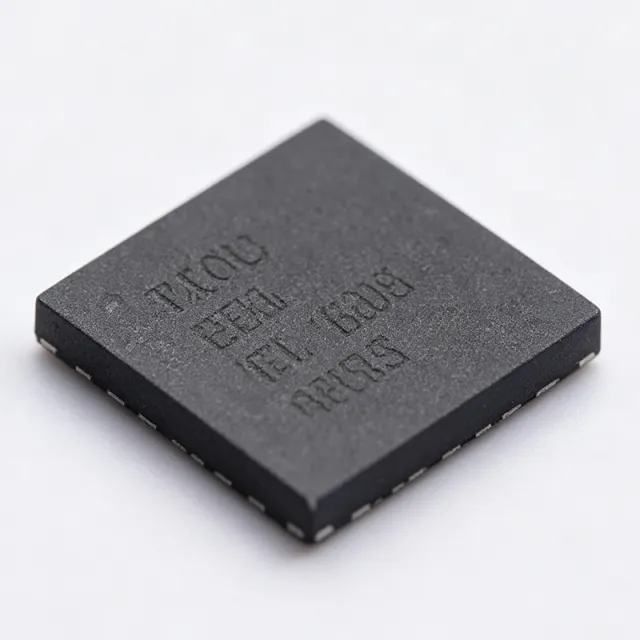
The Texas Instruments TIOL221 (TIOL221RGER) is a dual-channel IO-Link device physical layer (PHY) transceiver with an integrated LDO and SPI interface, supplied in a 24-pin VQFN (4x4 mm) package. It serves as the complete physical layer between an IO-Link master and a remote sensor or actuator node over the three-wire IO-Link interface (L+, L-, CQ). An IO-Link PHY (physical layer transceiver) is a specialized industrial communication interface IC that handles line driving, wake-up detection, and protection for point-to-point digital communication networks. Within the system hierarchy, it sits below the microcontroller (logic layer) and above the physical cabling, forming part of the broader industrial networking and sensor interface semiconductor category. Key features include dual CQ channels with integrated low-power output drivers featuring active reverse polarity protection, wake-up pulse generation and detection (sinking or sourcing >= 500 mA for a typical 80 us duration per IO-Link specification), and wake-up reporting to the local microcontroller by asserting the WU pin low. Internal protection covers undervoltage, overcurrent, and overtemperature conditions, with fault reporting to the host. The integrated LDO reduces external BOM count, and the SPI interface allows flexible configuration and diagnostics. The device can also be configured to generate wake-up pulses and be used in IO-Link master applications, and it integrates an auxiliary DI (digital input) channel. Typical applications include IO-Link sensor hubs, industrial proximity sensors, actuator nodes, and compact IO-Link master ports. Design tip: ensure the CQ driver thermal budget accounts for wake-up pulse current, and use the fault reporting pins for system-level diagnostics.

TIOL221RGER - Dual-Channel IO-Link PHY, LDO, SPI | Texas Instruments
The Texas Instruments TIOL221RGER is a dual-channel IO-Link device physical layer (PHY) transceiver integrating two low-power output drivers with active reverse polarity protection, an integrated LDO, and an SPI interface in a 24-pin VQFN (4x4 mm) package. It provides a complete physical layer for IO-Link communication over a three-wire interface for industrial sensors and actuators. An IO-Link transceiver is a specialized interface IC that bridges a local microcontroller to the IO-Link communication standard, enabling point-to-point communication between sensors or actuators and an IO-Link master. It converts MCU digital data into IO-Link physical layer signals on the CQ line and vice versa while adding power management and protection. In the component hierarchy it sits as: IO-Link PHY -> industrial communication interface -> sensor interface IC -> mixed-signal semiconductor. Key features include dual-channel operation for two independent IO-Link ports in one package, an integrated LDO that simplifies power design, SPI-based configuration and diagnostics, and wake-up support: the device can sink or source at least 500 mA for the wake-up duration (typically 80 microseconds) depending on the CQ logic level, then asserts the WU pin low for tWUL to notify the local MCU. Surge robustness reaches 1.2 kV (500 ohm) per IEC 61000-4-5. Technically, the TIOL221 provides fault reporting and internal protection for undervoltage, overcurrent, and overtemperature conditions, and can be configured to generate wake-up pulses, also supporting IO-Link master applications. An auxiliary DI channel adds digital input functionality. Active reverse polarity protection removes the need for external series diodes, reducing voltage drop and bill-of-material cost. Typical applications include industrial proximity, pressure, and temperature sensors, actuators, and IO-Link master port circuitry. The dual-channel capability halves board area versus two single-channel PHYs. Design tip: decouple the integrated LDO carefully and configure wake-up timing per the IO-Link specification; external TVS diodes may still be needed for surge levels beyond the built-in protection.
TJA1021TK/20/C - 20 kBd LIN Transceiver | NXP
The NXP TJA1021TK/20/C is an automotive LIN physical-layer transceiver supporting communication from 1 kBd to 20 kBd in an 8-pin HVSON package measuring 3 x 3 mm. It interfaces a LIN commander or responder protocol controller with the physical LIN bus, integrates a voltage regulator, and supports LIN 2.0, LIN 2.1, LIN 2.2, LIN 2.2A, SAE J2602, and ISO 17987-4:2016 communication. A LIN transceiver is a physical-layer interface IC within the broader automotive network-controller hierarchy. A microcontroller or dedicated LIN controller generates serial transmit data, while the transceiver converts that logic-level signal into a waveform suitable for the single-wire LIN bus. It also receives the bus waveform and converts it back into a logic signal that the protocol controller can interpret. The TJA1021TK/20/C provides optimized slew-rate control and waveform shaping to reduce electromagnetic emissions. It is pin-compatible with the TJA1020 and MC33662B families and has an improved electrostatic-discharge specification relative to the TJA1020. The integrated regulator reduces the external power-supply requirements of the transceiver. Its 20 kBd limit supports modern in-vehicle subnetworks while retaining compatibility with lower LIN baud rates down to 1 kBd. The /20 variant is intended for LIN networks operating at rates up to 20 kBd. The HVSON-8 package provides a compact surface-mount footprint and an exposed thermal pad for heat dissipation. Because a LIN bus is a single-wire network, its transceiver must coordinate transmitter dominance, receiver thresholds, bus termination, waveform control, and fault behavior while allowing multiple nodes to share the same communication channel. Typical uses include LIN master modules, LIN slave controllers, body-control modules, door modules, seat modules, climate-control interfaces, switch panels, automotive lighting controllers, and other low-speed vehicle subnetworks. The part is particularly suitable where compact placement, standardized LIN behavior, low electromagnetic emissions, and direct compatibility with existing TJA1020-class hardware are important. Design the LIN bus according to the NXP datasheet, including the specified transceiver input and output capacitors, bus termination, pull-up arrangement, wiring topology, and exposed-pad soldering. Maintain the required headroom between the battery-side supply and the LIN bus level, and validate EMC behavior in the finished vehicle harness because cable geometry and termination can affect edge quality. This page combines protocol compatibility, package details, verified sourcing information, drop-in alternatives, and practical integration guidance. It also identifies where design data must be checked against the manufacturer datasheet, helping engineers move from component selection to LIN network implementation more efficiently.

TJA1022T - Dual LIN 2.2A Transceiver | NXP Semiconductors
The NXP Semiconductors TJA1022T is a dual LIN transceiver that interfaces a Local Interconnect Network leader or follower protocol controller with the physical LIN bus. It supports LIN bus data rates up to 20 kBd and complies with LIN 2.0, LIN 2.1, LIN 2.2, LIN 2.2A, and SAE J2602. The device is supplied in the 14-pin SO14 surface-mount package identified by the TJA1022T ordering code. A LIN transceiver is a physical-layer interface IC within the broader automotive networking hierarchy. It connects a host microcontroller or LIN protocol controller to a low-speed, single-wire vehicle network by translating controller-side logic signals into LIN bus levels and receiving bus signals for the controller. Two integrated transceivers allow one controller to manage two LIN channels while retaining a common device footprint and application architecture. The TJA1022 is primarily intended for in-vehicle subnetworks operating at baud rates up to 20 kBd. Its stated compliance includes LIN 2.0, LIN 2.1, LIN 2.2, LIN 2.2A, and SAE J2602. These protocol and automotive-interface specifications make the TJA1022T relevant to distributed vehicle systems in which body, comfort, lighting, seat, door, and other accessory modules exchange commands and diagnostic information over LIN networks. The NXP datasheet identifies the TJA1022T and TJA1022TK as pin-compatible with the TJA1020, TJA1021, TJA1027, and TJA1029. It also states that the TJA1022, TJA1024, TJA1027, and TJA1029 are software compatible. These compatibility statements support platform reuse, although designers should still verify operating conditions, enabled features, electrical limits, and package dimensions for each selected order code before treating a part as a replacement. Typical uses include vehicle body-control modules, door and seat controllers, lighting controllers, climate-control interfaces, sensor nodes, and gateway modules that combine LIN communication with microcontroller processing. The dual-channel configuration can simplify boards that must connect multiple LIN subnets while reducing the number of separate physical-layer transceivers required. When designing around the TJA1022T, preserve the pin compatibility and protocol expectations of the selected TJA1020, TJA1021, TJA1027, or TJA1029 reference design. The LIN bus interface must be reviewed against the manufacturer datasheet for termination, wiring, protection, grounding, and application-specific guidance. This page combines verified manufacturer information, distributor availability, package details, and compatibility options for faster component selection. This product data adds practical context beyond basic catalog listings by organizing protocol compliance, package compatibility, verified alternative families, bus-focused applications, and sourcing information. It highlights where the TJA1022T fits in a LIN network while clearly separating verified facts from specifications that still require confirmation from the manufacturer datasheet.
TJA1028T/3V3/10 - 3.3V LIN Transceiver with 70mA Regulator
The NXP Semiconductors TJA1028T/3V3/10 is a LIN bus transceiver with an integrated 3.3 V low-dropout voltage regulator capable of delivering up to 70 mA, housed in an 8-pin SOIC package. It combines LIN 2.0, LIN 2.1, SAE J2602, and ISO 17987-4:2016 for 12 V systems with local power delivery for compact automotive and industrial LIN nodes. A LIN transceiver is a physical-layer interface for the Local Interconnect Network, a low-cost, single-wire serial bus commonly used to connect sensors, actuators, door modules, climate controls, and other distributed automotive electronics. The TJA1028 combines that bus interface with a 3.3 V regulator, reducing the number of components required at a compact LIN slave node. The headline features are compliance with LIN 2.0, LIN 2.1, SAE J2602, and ISO 17987-4:2016, a regulated 3.3 V output rated to 70 mA, and an 8-pin SOIC package. The integrated regulator allows a peripheral device to receive local supply from the LIN system while the transceiver communicates over the same harness. The TJA1028 family is designed for compact nodes connected to 12 V LIN networks. Its integrated regulator supports the 3.3 V variant identified by the /3V3 ordering code, while the TJA1028 family also includes a 5.0 V regulator variant. This distinction is important because replacing the 3.3 V device with the 5.0 V device changes the local supply presented to attached circuitry. Typical uses include LIN-connected sensor modules, body-control submodules, automotive door and seat electronics, climate-control nodes, and industrial control modules that use LIN for inexpensive short-range networking. Compactness and local supply integration are particularly valuable when the node must fit behind a vehicle trim panel or within a sealed enclosure. When designing a TJA1028T/3V3/10 circuit, follow the NXP datasheet wiring and decoupling recommendations, preserve the transceiver's LIN bus and ground connections, and validate the regulator load transient response at the maximum 70 mA operating point. Check the package pin assignments against the selected PCB footprint before layout. This product overview consolidates the manufacturer-defined LIN compliance, integrated 3.3 V regulator capability, package information, sourcing guidance, and engineering considerations into one reference for compact LIN-node development.
TJA1040T/H/V - 1 Mbps CAN Transceiver | NXP Semiconductors
The NXP Semiconductors TJA1040T/H/V is a high-speed CAN physical-layer transceiver designed for passenger-car CAN networks operating up to 1 MBaud. It provides a differential transmitter for the CAN bus and a differential receiver for the CAN controller, with an 8-pin SOIC package. The device is intended for systems where the protocol controller performs CAN frame handling while the transceiver converts digital controller signals into the physical differential bus waveform. A CAN transceiver is an interface IC that connects a CAN protocol controller to the physical bus. The TJA1040T/H/V belongs to the CAN transceiver class, also described as a CAN physical-layer interface, interface IC, and CAN bus transceiver. It supports the differential signaling used by high-speed CAN systems, allowing controller-side TXD and RXD signals to interface with the CANH and CANL bus conductors. The principal device characteristics include a maximum intended CAN data rate of 1 MBaud, a half-duplex CAN transceiver arrangement, differential transmit capability, and differential receive capability. The 8-SO package supports conventional surface-mount PCB assembly. The TJA1040 family is intended for automotive and other CAN-based passenger-car applications where the physical-layer transceiver must operate alongside a separate CAN protocol controller. The transceiver architecture separates protocol processing from bus-line interfacing: the CAN controller generates and interprets frames, while the TJA1040T/H/V handles the electrical signaling between logic-level pins and the CAN bus. This division allows the controller to manage arbitration, acknowledgment, error handling, and higher-layer communication independently of the physical-layer conversion performed by the transceiver. Typical applications include automotive electronic control units, body-control modules, powertrain controllers, gateway modules, engine controllers, and other distributed vehicle systems. The same high-speed CAN physical interface can also be used in industrial, robotics, and transportation equipment when the system uses a compatible CAN controller and bus topology. Designers should verify the device pinout, supply requirements, CANH and CANL connections, termination strategy, and the exact ordering-code interpretation in the manufacturer datasheet before layout release. For PCB work, use the SOIC-8 land pattern and route the differential bus pair with consistent geometry and symmetry. The CAN bus should be properly terminated at the physical ends of the network, and the power and ground connections should follow the datasheet recommendations. This page combines the NXP product description, manufacturer data-sheet reference, cross-reference findings, package information, practical application guidance, and structured comparisons for engineers evaluating the TJA1040T/H/V in a high-speed CAN design.

TJA1042 - 5 Mbit/s High-Speed CAN FD Transceiver | NXP
The NXP Semiconductors TJA1042 is a high-speed CAN transceiver that provides the interface between a CAN protocol controller and the physical two-wire CAN bus. It implements the CAN physical layer as defined in ISO 11898-2:2016 and SAE J2284-1 to J2284-5, supporting reliable communication in the CAN FD fast phase at data rates up to 5 Mbit/s. The typical orderable version, TJA1042T/3,118, comes in an 8-pin SOIC package. A CAN transceiver is the physical-layer device that converts controller TXD/RXD logic levels into differential bus signals (CANH/CANL) and back. Within the interface IC hierarchy, it sits between the microcontroller CAN peripheral and the bus wiring, and is essential for robust automotive and industrial networking in electrically noisy environments. Key features include a Standby mode with very low current consumption for always-on, wake-on-CAN applications; undervoltage detection on VCC; a SPLIT pin that stabilizes the recessive bus level on long networks; improved slope control; and high DC handling capability on the bus pins. As a third-generation NXP transceiver, the TJA1042 combines the functionality of the PCA82C250, PCA82C251 and TJA1040 with improved EMC and ESD performance and lower quiescent current. Thermal shutdown protection and wide supply tolerance further increase robustness. Architecturally, the TJA1042 uses a differential transceiver core with integrated common-mode stabilization and slope control, meeting demanding automotive EMC requirements without external filtering in most designs. Typical applications include automotive body control modules, gateway modules, engine control units, and industrial automation systems requiring standards-compliant CAN or CAN FD communication. Standby mode directly benefits nodes that must wake on bus activity while minimizing sleep current. Design tip: terminate the bus with 120 ohms at each end, keep the transceiver close to the connector to minimize stub length, and follow NXP application hint document AH1308 for SPLIT-pin usage to improve signal integrity on long bus lines.