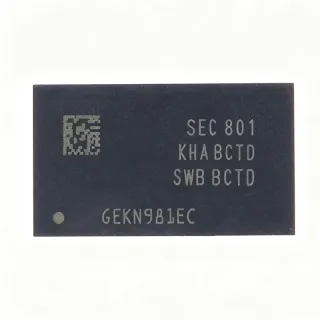
K4B4G1646D-BCH90 - 4Gb DDR3L SDRAM x16 96FBGA | Samsung
MPN: K4B4G1646D-BCH90 ✓ فعالK4B4G1646D-BCH90 نمای کلی
DDR3L (Low Voltage DDR3) is a type of synchronous dynamic random-access memory that operates at a lower voltage (1.35V) compared to standard DDR3 (1.5V), reducing power consumption by about 20% while maintaining similar performance. It is part of the DDR3 SDRAM family, which uses double data rate architecture to transfer data on both edges of the clock, and is widely used in computing, networking, and embedded systems.
Key features include programmable CAS latency, write latency, on-die termination (ODT), and internal calibration (ZQ calibration) for signal integrity. The device supports auto precharge, asynchronous reset, and data mask functions. It is lead-free and halogen-free, RoHS compliant, and operates over a temperature range of 0°C to +85°C.
The K4B4G1646D-BCH90 uses a D-die process, offering improved performance and power efficiency. The 96-ball FBGA package provides a compact footprint with excellent thermal and electrical characteristics. The device supports burst lengths of 8 and 4, and features programmable CAS latency from 9 to 14 clocks.
Typical applications include mobile devices, consumer electronics, networking equipment, and embedded systems where low power and high density are critical. The 1.35V operation makes it ideal for battery-powered devices, while the high-speed interface supports bandwidth-intensive tasks.
When designing with this device, ensure proper decoupling and signal integrity practices, including controlled impedance traces and termination. The ZQ calibration pin requires a 240-ohm resistor to ground for accurate on-die termination calibration.
جایگزینهای drop-in برای K4B4G1646D-BCH90 — همان پکیج، سازگار پینبهپین. قطعات با پکیج متفاوت که نیاز به تغییر PCB دارند مستثنی هستند.
گونهها در این سری
مدلهای همسری که جایگزین مستقیم هستند برای K4B4G1646D-BCH90 (همان فرمفاکتور و فوتپرینت) — متفاوت در Supply Voltage, CAS Latency, Package, Burst Length, Data Rate.
K4B4G1646D-BHMA
✅ جایگزین مستقیمبرای قیمت تماس بگیرید
مشاهده دیتاشیت ←K4B4G1646D-BYK0
✅ جایگزین مستقیمبرای قیمت تماس بگیرید
مشاهده دیتاشیت ←K4B4G1646D-BCMA
✅ جایگزین مستقیم📋 جایگزین مرجع (خارج از کاتالوگ)
K4B4G1646D-BFMA
✅ جایگزین مستقیمبرای قیمت تماس بگیرید
مشاهده دیتاشیت ←K4B4G1646E-BMMA
✅ جایگزین مستقیمبرای قیمت تماس بگیرید
مشاهده دیتاشیت ←MT41K256M16HA-125
✅ جایگزین مستقیم ⚠️ مشخصات تأییدنشدهبرای قیمت تماس بگیرید
مشاهده دیتاشیت ←H5TC4G63AFR
✅ جایگزین مستقیم ⚠️ مشخصات تأییدنشده📋 جایگزین مرجع (خارج از کاتالوگ)
K4B4G1646D-BCH90 حداکثر مقادیر مجاز و مشخصات الکتریکی
| نوع حافظه | DDR3L SDRAM |
| Density | 4Gb |
| سازمان | 32M x 16 |
| Number of Banks | 8 |
| نرخ داده | 2133 Mb/s per pin |
| ولتاژ تغذیه | 1.35V (1.283V to 1.45V) |
| بستهبندی | 96-ball FBGA |
| دمای کاری | 0°C to +85°C |
| تأخیر CAS | 9-14 clocks (programmable) |
| Burst Length | 8 and 4 |
| On-Die Termination | Yes (ODT) |
| ZQ Calibration | Yes |
| Auto Precharge | Yes |
| Asynchronous Reset | Yes |
| Data Mask | Yes |
| RoHS Compliant | Yes |
| Lead-Free | Yes |
| بدون هالوژن | Yes |
پیکربندی پین K4B4G1646D-BCH90
| پین A1 | VDD — Power supply |
| پین A2 | DQ0 — Data input/output 0 |
| پین A3 | DQ1 — Data input/output 1 |
| پین A4 | VSS — Ground |
| پین A5 | DQ2 — Data input/output 2 |
| پین A6 | DQ3 — Data input/output 3 |
| پین A7 | VDD — Power supply |
| پین A8 | DQ4 — Data input/output 4 |
| پین A9 | DQ5 — Data input/output 5 |
| پین A10 | VSS — Ground |
| پین A11 | DQ6 — Data input/output 6 |
| پین A12 | DQ7 — Data input/output 7 |
| پین B1 | VSS — Ground |
| پین B2 | DQ8 — Data input/output 8 |
| پین B3 | DQ9 — Data input/output 9 |
| پین B4 | VDD — Power supply |
| پین B5 | DQ10 — Data input/output 10 |
| پین B6 | DQ11 — Data input/output 11 |
| پین B7 | VSS — Ground |
| پین B8 | DQ12 — Data input/output 12 |
| پین B9 | DQ13 — Data input/output 13 |
| پین B10 | VDD — Power supply |
| پین B11 | DQ14 — Data input/output 14 |
| پین B12 | DQ15 — Data input/output 15 |
| پین C1 | VDDQ — I/O power supply |
| پین C2 | VSSQ — I/O ground |
| پین C3 | VDDQ — I/O power supply |
| پین C4 | VSSQ — I/O ground |
| پین C5 | VDDQ — I/O power supply |
| پین C6 | VSSQ — I/O ground |
| پین C7 | VDDQ — I/O power supply |
| پین C8 | VSSQ — I/O ground |
| پین C9 | VDDQ — I/O power supply |
| پین C10 | VSSQ — I/O ground |
| پین C11 | VDDQ — I/O power supply |
| پین C12 | VSSQ — I/O ground |
| پین D1 | A0 — Address input 0 |
| پین D2 | A1 — Address input 1 |
| پین D3 | A2 — Address input 2 |
| پین D4 | A3 — Address input 3 |
| پین D5 | A4 — Address input 4 |
| پین D6 | A5 — Address input 5 |
| پین D7 | A6 — Address input 6 |
| پین D8 | A7 — Address input 7 |
| پین D9 | A8 — Address input 8 |
| پین D10 | A9 — Address input 9 |
| پین D11 | A10/AP — Address input 10 / auto precharge |
| پین D12 | A11 — Address input 11 |
| پین E1 | A12 — Address input 12 |
| پین E2 | A13 — Address input 13 |
| پین E3 | A14 — Address input 14 |
| پین E4 | BA0 — Bank address 0 |
| پین E5 | BA1 — Bank address 1 |
| پین E6 | BA2 — Bank address 2 |
| پین E7 | RAS# — Row address strobe |
| پین E8 | CAS# — Column address strobe |
| پین E9 | WE# — Write enable |
| پین E10 | CS# — Chip select |
| پین E11 | CKE — Clock enable |
| پین E12 | ODT — On-die termination |
| پین F1 | CK — Clock |
| پین F2 | CK# — Complementary clock |
| پین F3 | VDD — Power supply |
| پین F4 | VSS — Ground |
| پین F5 | VDD — Power supply |
| پین F6 | VSS — Ground |
| پین F7 | VDD — Power supply |
| پین F8 | VSS — Ground |
| پین F9 | VDD — Power supply |
| پین F10 | VSS — Ground |
| پین F11 | VDD — Power supply |
| پین F12 | VSS — Ground |
| پین G1 | DM0 — Data mask 0 |
| پین G2 | DM1 — Data mask 1 |
| پین G3 | VSS — Ground |
| پین G4 | VDD — Power supply |
| پین G5 | VSS — Ground |
| پین G6 | VDD — Power supply |
| پین G7 | VSS — Ground |
| پین G8 | VDD — Power supply |
| پین G9 | VSS — Ground |
| پین G10 | VDD — Power supply |
| پین G11 | VSS — Ground |
| پین G12 | VDD — Power supply |
| پین H1 | ZQ — Calibration reference |
| پین H2 | VSS — Ground |
| پین H3 | VDD — Power supply |
| پین H4 | VSS — Ground |
| پین H5 | VDD — Power supply |
| پین H6 | VSS — Ground |
| پین H7 | VDD — Power supply |
| پین H8 | VSS — Ground |
| پین H9 | VDD — Power supply |
| پین H10 | VSS — Ground |
| پین H11 | VDD — Power supply |
| پین H12 | VSS — Ground |
| پین J1 | NC — No connect |
| پین J2 | NC — No connect |
| پین J3 | NC — No connect |
| پین J4 | NC — No connect |
| پین J5 | NC — No connect |
| پین J6 | NC — No connect |
| پین J7 | NC — No connect |
| پین J8 | NC — No connect |
| پین J9 | NC — No connect |
| پین J10 | NC — No connect |
| پین J11 | NC — No connect |
| پین J12 | NC — No connect |
کاربردهای معمول
K4B4G1646D-BCH90 مناسب است برای 6 کاربردs: Mobile Devices, Consumer Electronics, Networking Equipment, Embedded Systems, Computing Systems, Automotive Infotainment.
Mobile Devices
The K4B4G1646D-BCH90's low 1.35V operation and 4Gb density make it ideal for smartphones and tablets where power efficiency and compact size are critical. Its 2133Mb/s data rate supports high-bandwidth applications like HD video and gaming. The 96-ball FBGA package fits tight PCB layouts, and the commercial temperature range covers typical mobile use cases.
پیشنهادی
Consumer Electronics
In consumer devices like smart TVs, set-top boxes, and gaming consoles, the K4B4G1646D-BCH90 provides the memory bandwidth needed for smooth multimedia playback and responsive user interfaces. Its 4Gb density supports multiple applications simultaneously, while the low voltage reduces overall system power. The FBGA package enables slim product designs.
پیشنهادی
Networking Equipment
Routers, switches, and network appliances require high-speed memory for packet buffering and routing tables. The K4B4G1646D-BCH90's 2133Mb/s data rate and 4Gb density provide ample bandwidth and capacity. Its low power consumption is beneficial in always-on networking gear, and the commercial temperature range suits indoor environments.
پیشنهادی
Embedded Systems
For industrial and embedded applications, the K4B4G1646D-BCH90 offers reliable DDR3L memory with a wide operating temperature range (0°C to +85°C). Its 4Gb density supports complex firmware and data logging. The 96-ball FBGA package is robust for harsh environments, and the low voltage reduces heat generation.
پیشنهادی
Computing Systems
In laptops, mini-PCs, and servers, the K4B4G1646D-BCH90 provides high-density, low-power memory for multitasking and data-intensive workloads. Its 2133Mb/s speed ensures fast data access, while the 1.35V operation extends battery life in portable devices. The FBGA package is standard for SODIMM and board-down designs.
پیشنهادی
Automotive Infotainment
Although the K4B4G1646D-BCH90 has a commercial temperature range, it can be used in automotive infotainment systems with proper thermal management. Its 4Gb density supports navigation, multimedia, and connectivity features. The low power consumption is beneficial for vehicle electrical systems, and the FBGA package withstands vibration.
پیشنهادی
خلاصه محصولات پیشنهادی
دادههای مرجع مهندسی برای K4B4G1646D-BCH90 — مقایسه، راهنمای طراحی و اطلاعات انطباق.
راهنمای انتخاب
مقایسه با جایگزینها
| پارامتر | این محصول | K4B4G1646D-BHMA | K4B4G1646D-BYK0 | K4B4G1646E-BMMA | MT41K256M16HA-125 |
|---|---|---|---|---|---|
| Package | 96-ball FBGA | 96-ball FBGA | 96-ball FBGA | 96-ball FBGA | 96-ball FBGA |
| Brand | Samsung Electronics | Samsung Electronics | Samsung Electronics | Samsung Electronics | Micron Technology |
| Density | 4Gb | 4Gb | 4Gb | 4Gb | 4Gb |
| Organization | 32M x 16 | 32M x 16 | 32M x 16 | 32M x 16 | 32M x 16 |
| Supply Voltage | 1.35V | 1.35V | 1.35V | 1.35V | 1.35V |
| Operating Temperature | 0°C to +85°C | 0°C to +85°C | 0°C to +85°C | 0°C to +85°C | 0°C to +95°C |
| RoHS Compliant | Yes | Yes | Yes | Yes | Yes |
تفاوتهای کلیدی
- Low voltage operation at 1.35V (در مقابلMT41K256M16HA-125)
- High data rate of 2133Mb/s (در مقابلMT41K256M16HA-125)
- D-die process technology (در مقابلK4B4G1646E-BMMA)
یادداشتهای طراحی
For reliable DDR3L operation, maintain controlled impedance of 40-50 ohms for data lines and 50-60 ohms for address/control lines. Keep trace lengths matched within 100 mils for each byte lane. Place decoupling capacitors (0.1uF and 0.01uF) close to each VDD and VDDQ pin, and a 10uF bulk capacitor near the memory power supply.
Use on-die termination (ODT) settings to match the memory bus impedance. The ZQ pin requires a 240-ohm resistor to ground for calibration. Ensure the reference voltage (VREF) is clean and stable, typically generated by a resistor divider or dedicated regulator. Follow the layout guidelines in the Samsung datasheet for optimal signal integrity.
The K4B4G1646D-BCH90 operates up to +85°C. In high-density designs, ensure adequate airflow or a thermal pad to dissipate heat. The FBGA package has a thermal resistance that should be considered; refer to the datasheet for theta_JA values. For automotive or industrial environments, consider a wider temperature grade if available.
اطلاعات انطباق
RoHS compliant, lead-free, and halogen-free per Samsung datasheet. AEC-Q100 not applicable for memory components.