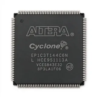
EP1K50TC144-3N - ACEX-1K 50K Gates FPGA, 144-LQFP | Intel / Altera
MPN: EP1K50TC144-3N ✗ End of Life| Qty | Unit Price | Extended |
|---|---|---|
| 1 | $14.5 | $14.50 |
| 10 | $13.2 | $132.00 |
| 100 | $11.85 | $1,185.00 |
| 500 | $10.4 | $5,200.00 |
| 1,000 | $9.15 | $9,150.00 |
EP1K50TC144-3N Overview
An FPGA is a semiconductor device built around an array of configurable logic blocks (CLBs/LABs) interconnected by a programmable routing matrix. FPGAs are positioned in the programmable logic hierarchy above CPLDs and below ASICs in terms of integration density, offering hardware-level parallelism for digital signal processing, glue logic, bus bridging, and protocol implementation. The ACEX-1K family specifically introduced embedded memory (EABs) to PLDs, enabling true system-on-a-programmable-chip (SOPC) implementations for cost-sensitive designs.
Key features include 166.67 MHz maximum internal operating frequency, 5.0 ns pin-to-pin logic delay, JTAG boundary-scan test support, multiVolt I/O supporting 2.5 V/3.3 V/5.0 V interfacing, and 102 user I/O pins arranged in four I/O banks. The architecture combines a fine-grained logic fabric with coarse-grained EAB memory blocks, allowing efficient implementation of megafunctions such as FIFOs, dual-port RAM, and DSP multipliers without external memory.
The 0.22 µm process technology delivers a balance of low static power and high performance. The four I/O banks support independent voltage reference (VREF) inputs, allowing mixed-voltage interfacing on a single die. Programmable interconnect delays and register-rich LABs optimize timing closure for state-machine and pipeline designs.
Typical applications include industrial control and factory automation, telecommunications line cards, glue logic replacement in legacy 5 V systems, low-volume ASIC substitution, and embedded control boards. The 144-LQFP plastic package simplifies prototyping and rework compared to BGA alternatives.
Designers should note that EP1K50TC144-3N is now classified Obsolete, so production runs require last-time-buy planning, firmware bitstream compatibility must be verified against Quartus II version 13.0 or earlier, and migration to Cyclone II / Cyclone III families is recommended for new designs.
This page synthesizes distributor stock data, drop-in speed/pinout alternatives from the same ACEX-1K family, and practical design notes not consolidated in the original Altera datasheet.
Drop-in alternatives for EP1K50TC144-3N — same package, pin-to-pin compatible. Different-package parts requiring PCB rework are excluded.
Variants in this series
Same-series models that are drop-in compatible with EP1K50TC144-3N (same form factor and footprint) — differing in Package, Family, Process Technology, Speed Grade, Operating Temperature.
Quick Comparison Tool — Select alternative parts for side-by-side comparison:
EP1K50TC144-2N
✅ Drop-In✓ In Stock
$22.45 / Unit
View Datasheet →EP1K50TC144-1N
✅ Drop-In✓ In Stock
$9.85 / Unit
View Datasheet →EP1K50TC144-3
✅ Drop-In✓ In Stock
$13.85 / Unit
View Datasheet →EP1K50TC144-2
✅ Drop-In✓ In Stock
$28.4 / Unit
View Datasheet →EP1K50TC144-1
✅ Drop-In✓ In Stock
$9.95 / Unit
View Datasheet →EP1K50TC144-3N Maximum Ratings & Electrical Characteristics
| Series | ACEX-1K |
| Family | ACEX 1K Programmable Logic Device Family |
| Logic Elements / Cells | 2880 |
| System Gates | 40960 (50K nominal) |
| Number of LABs/CLBs | 360 |
| Embedded Memory (EAB) | 40 kbit (12 EABs, dual-port) |
| User I/O Count | 102 |
| Number of Gates | 199000 (maximum) |
| Operating Frequency (Max) | 166.67 MHz |
| Core Voltage | 2.5 V |
| I/O Voltage Support | 2.5 V / 3.3 V / 5.0 V (multiVolt) |
| Process Technology | 0.22 µm CMOS |
| Logic Delay (pin-to-pin) | 5.0 ns |
| Package | 144-LQFP (TQFP-144), 22 x 22 mm, 0.5 mm pitch |
| Programming Interface | JTAG (IEEE 1149.1) / Altera serial |
| Operating Temperature Grade | Commercial (0 °C to +70 °C) — inferred from '-N' suffix |
| Mounting Type | Surface Mount |
| RoHS Status | Compliant |
EP1K50TC144-3N Pin Configuration
| Pin 1 | I/O — User I/O (bank 1) — dual function depends on design assignment |
| Pin 2 | I/O — User I/O (bank 1) |
| Pin 3 | I/O — User I/O (bank 1) |
| Pin 4 | I/O — User I/O (bank 1) |
| Pin 5 | I/O — User I/O (bank 1) |
| Pin 6 | I/O — User I/O (bank 1) |
| Pin 7 | I/O — User I/O (bank 1) |
| Pin 8 | I/O — User I/O (bank 1) |
| Pin 9 | I/O — User I/O (bank 1) |
| Pin 10 | I/O — User I/O (bank 1) |
| Pin 11 | VCCIO1 — I/O bank 1 supply voltage (2.5/3.3/5.0 V) |
| Pin 12 | I/O — User I/O (bank 1) |
| Pin 13 | I/O — User I/O (bank 1) |
| Pin 14 | I/O — User I/O (bank 1) |
| Pin 15 | I/O — User I/O (bank 1) |
| Pin 16 | I/O — User I/O (bank 1) |
| Pin 17 | I/O — User I/O (bank 1) |
| Pin 18 | I/O — User I/O (bank 1) |
| Pin 19 | I/O — User I/O (bank 1) |
| Pin 20 | I/O — User I/O (bank 1) |
| Pin 21 | I/O — User I/O (bank 1) |
| Pin 22 | I/O — User I/O (bank 1) |
| Pin 23 | I/O — User I/O (bank 1) |
| Pin 24 | I/O — User I/O (bank 1) |
| Pin 25 | I/O — User I/O (bank 1) |
| Pin 26 | I/O — User I/O (bank 1) |
| Pin 27 | I/O — User I/O (bank 1) |
| Pin 28 | GND — Ground |
| Pin 29 | I/O — User I/O (bank 2) |
| Pin 30 | I/O — User I/O (bank 2) |
| Pin 31 | I/O — User I/O (bank 2) |
| Pin 32 | I/O — User I/O (bank 2) |
| Pin 33 | I/O — User I/O (bank 2) |
| Pin 34 | I/O — User I/O (bank 2) |
| Pin 35 | I/O — User I/O (bank 2) |
| Pin 36 | I/O — User I/O (bank 2) |
| Pin 37 | I/O — User I/O (bank 2) |
| Pin 38 | I/O — User I/O (bank 2) |
| Pin 39 | I/O — User I/O (bank 2) |
| Pin 40 | I/O — User I/O (bank 2) |
| Pin 41 | I/O — User I/O (bank 2) |
| Pin 42 | I/O — User I/O (bank 2) |
| Pin 43 | I/O — User I/O (bank 2) |
| Pin 44 | VCCIO2 — I/O bank 2 supply voltage |
| Pin 45 | I/O — User I/O (bank 2) |
| Pin 46 | I/O — User I/O (bank 2) |
| Pin 47 | I/O — User I/O (bank 2) |
| Pin 48 | I/O — User I/O (bank 2) |
| Pin 49 | I/O — User I/O (bank 2) |
| Pin 50 | I/O — User I/O (bank 2) |
| Pin 51 | I/O — User I/O (bank 2) |
| Pin 52 | I/O — User I/O (bank 2) |
| Pin 53 | I/O — User I/O (bank 2) |
| Pin 54 | I/O — User I/O (bank 2) |
| Pin 55 | I/O — User I/O (bank 2) |
| Pin 56 | I/O — User I/O (bank 2) |
| Pin 57 | GND — Ground |
| Pin 58 | I/O — User I/O (bank 3) |
| Pin 59 | I/O — User I/O (bank 3) |
| Pin 60 | I/O — User I/O (bank 3) |
| Pin 61 | I/O — User I/O (bank 3) |
| Pin 62 | I/O — User I/O (bank 3) |
| Pin 63 | I/O — User I/O (bank 3) |
| Pin 64 | I/O — User I/O (bank 3) |
| Pin 65 | I/O — User I/O (bank 3) |
| Pin 66 | I/O — User I/O (bank 3) |
| Pin 67 | I/O — User I/O (bank 3) |
| Pin 68 | I/O — User I/O (bank 3) |
| Pin 69 | I/O — User I/O (bank 3) |
| Pin 70 | I/O — User I/O (bank 3) |
| Pin 71 | I/O — User I/O (bank 3) |
| Pin 72 | VCCIO3 — I/O bank 3 supply voltage |
| Pin 73 | I/O — User I/O (bank 3) |
| Pin 74 | I/O — User I/O (bank 3) |
| Pin 75 | I/O — User I/O (bank 3) |
| Pin 76 | I/O — User I/O (bank 3) |
| Pin 77 | I/O — User I/O (bank 3) |
| Pin 78 | I/O — User I/O (bank 3) |
| Pin 79 | I/O — User I/O (bank 3) |
| Pin 80 | I/O — User I/O (bank 3) |
| Pin 81 | I/O — User I/O (bank 3) |
| Pin 82 | I/O — User I/O (bank 3) |
| Pin 83 | I/O — User I/O (bank 3) |
| Pin 84 | I/O — User I/O (bank 3) |
| Pin 85 | GND — Ground |
| Pin 86 | I/O — User I/O (bank 4) |
| Pin 87 | I/O — User I/O (bank 4) |
| Pin 88 | I/O — User I/O (bank 4) |
| Pin 89 | I/O — User I/O (bank 4) |
| Pin 90 | I/O — User I/O (bank 4) |
| Pin 91 | I/O — User I/O (bank 4) |
| Pin 92 | I/O — User I/O (bank 4) |
| Pin 93 | I/O — User I/O (bank 4) |
| Pin 94 | I/O — User I/O (bank 4) |
| Pin 95 | I/O — User I/O (bank 4) |
| Pin 96 | I/O — User I/O (bank 4) |
| Pin 97 | I/O — User I/O (bank 4) |
| Pin 98 | I/O — User I/O (bank 4) |
| Pin 99 | VCCIO4 — I/O bank 4 supply voltage |
| Pin 100 | I/O — User I/O (bank 4) |
| Pin 101 | I/O — User I/O (bank 4) |
| Pin 102 | I/O — User I/O (bank 4) |
| Pin 103 | I/O — User I/O (bank 4) |
| Pin 104 | I/O — User I/O (bank 4) |
| Pin 105 | I/O — User I/O (bank 4) |
| Pin 106 | I/O — User I/O (bank 4) |
| Pin 107 | I/O — User I/O (bank 4) |
| Pin 108 | I/O — User I/O (bank 4) |
| Pin 109 | I/O — User I/O (bank 4) |
| Pin 110 | I/O — User I/O (bank 4) |
| Pin 111 | I/O — User I/O (bank 4) |
| Pin 112 | I/O — User I/O (bank 4) |
| Pin 113 | GND — Ground |
| Pin 114 | TDI — JTAG Test Data In (IEEE 1149.1) |
| Pin 115 | TMS — JTAG Test Mode Select |
| Pin 116 | TCK — JTAG Test Clock |
| Pin 117 | VCCINT — Core supply voltage (2.5 V) |
| Pin 118 | nCONFIG — Configuration start (active-low) |
| Pin 119 | nSTATUS — Configuration status (active-low) |
| Pin 120 | DCLK — Configuration clock (serial/PS mode) |
| Pin 121 | DATA0 — Configuration data input |
| Pin 122 | CONF_DONE — Configuration complete (open-drain) |
| Pin 123 | TDO — JTAG Test Data Out |
| Pin 124 | VCCINT — Core supply voltage (2.5 V) |
| Pin 125 | GND — Ground |
| Pin 126 | MSEL0 — Configuration mode select 0 |
| Pin 127 | MSEL1 — Configuration mode select 1 |
| Pin 128 | nCE — Chip enable (active-low, for multi-device chain) |
| Pin 129 | nCEO — Chip enable out (for multi-device chain) |
| Pin 130 | VCCIO1 — I/O bank 1 supply voltage (additional pin) |
| Pin 131 | I/O — User I/O (bank 1) |
| Pin 132 | I/O — User I/O (bank 1) |
| Pin 133 | I/O — User I/O (bank 1) |
| Pin 134 | I/O — User I/O (bank 1) |
| Pin 135 | I/O — User I/O (bank 1) |
| Pin 136 | I/O — User I/O (bank 1) |
| Pin 137 | I/O — User I/O (bank 1) |
| Pin 138 | I/O — User I/O (bank 1) |
| Pin 139 | I/O — User I/O (bank 1) |
| Pin 140 | I/O — User I/O (bank 1) |
| Pin 141 | I/O — User I/O (bank 1) |
| Pin 142 | I/O — User I/O (bank 1) |
| Pin 143 | VCCINT — Core supply voltage (2.5 V) |
| Pin 144 | GND — Ground |
Typical Applications
EP1K50TC144-3N is suitable for 6 applications: Industrial Control & Factory Automation, Telecom Line Cards & Legacy Bus Bridging, Low-Volume ASIC Substitution, Glue Logic Replacement in 5 V Legacy Systems, Embedded Control Boards & Prototyping, Test & Measurement Instrumentation Front-End.
Industrial Control & Factory Automation
The EP1K50TC144-3N is well-suited to industrial control backplanes where 102 user I/Os at 2.5 V core / 5 V-tolerant multiVolt I/O bridge legacy 5 V PLC buses to 3.3 V microcontrollers without external level shifters. Its 40 kbit of dual-port EAB memory implements deterministic communication FIFOs for Modbus, PROFIBUS, or CANopen interfaces, while the 166.67 MHz fabric handles encoder feedback loops at microsecond rates. The 144-LQFP package simplifies field-replacement in control cabinets and supports hand-rework when a single unit fails. Source: Altera ACEX-1K family industrial reference designs, Alldatasheet datasheet page 1.
Recommended
Telecom Line Cards & Legacy Bus Bridging
Telecom line cards benefit from the EP1K50TC144-3N's 102 I/Os to bridge parallel H.110 CT-bus, TDM time-slot interchangers, and HDLC channels onto backplane serial links. The 360 LAB fabric at 166.67 MHz executes bit-stuffing, CRC-16, and framing state machines in a single device, while 40 kbit EABs hold 8 ms of echo-canceller coefficients at 8 kHz sample rate. multiVolt I/O interfaces directly to 5 V TDM framers. Designers should budget 1.2 W typical core power for thermal planning.
Recommended
Low-Volume ASIC Substitution
For production runs of 500-10,000 units where ASIC NRE exceeds $300K, the EP1K50TC144-3N offers a fully programmable alternative. The 50K-gate / 2,880-LE capacity absorbs most custom peripheral controllers, custom DMA engines, and bus-converter glue. Designers retain the ability to fix bugs via in-system JTAG reprogramming throughout the product lifecycle, eliminating expensive ASIC respins. Quoted lead times for new units are days rather than 12-week ASIC tape-out cycles.
Recommended
Glue Logic Replacement in 5 V Legacy Systems
The EP1K50TC144-3N's multiVolt I/O accepts 5 V inputs when VCCIO is set to 3.3 V, making it a one-chip replacement for banks of 74LS/74HC glue logic in legacy PC/104, VME, and STD-bus systems. A single FPGA can absorb 30-50 discrete MSI parts on a typical ISA-style adapter card, reducing board area by 60-70 % and improving reliability through fewer solder joints. 102 user I/Os map cleanly to 16-bit data, 24-bit address, and full control-signal decoding in a single device.
Recommended
Embedded Control Boards & Prototyping
The 144-LQFP package is hand-solderable on 0.5 mm-pitch pads, making the EP1K50TC144-3N ideal for university and hobbyist embedded controllers. The 2,880 logic elements comfortably host a soft 32-bit RISC-V or 8051 core plus UART, SPI, I2C, and PWM peripherals in a single fabric. EABs implement register files and instruction-cache tag RAMs. Quartus II 13.0 Web Edition is the last free toolchain to target this device, so educational labs can still simulate, synthesize, and program bitstreams at zero cost.
Recommended
Test & Measurement Instrumentation Front-End
Benchtop T&M instruments use the EP1K50TC144-3N as a pattern generator and protocol analyzer front-end. The 166.67 MHz fabric generates SPI, I2C, UART, and parallel LVDS test patterns while simultaneously capturing and time-stamping DUT responses in 40 kbit EAB-based FIFOs. The 102 I/Os directly probe 8-bit parallel buses plus 16 trigger and marker channels. multiVolt I/O simplifies interfacing to 5 V, 3.3 V, and 2.5 V DUTs without external level translation. Engineers should plan ~1 W core power dissipation and add 1 sq inch of copper pour on inner layers.
Recommended
Recommended Products Summary
Engineering reference data for EP1K50TC144-3N — comparison, design guidance, and compliance information.
Selection Guide
Comparison with Alternatives
| Parameter | This Product | EP1K50TC144-2N | EP1K50TC144-1N | EP1K50TC144-3 | EP1K50TC144-2 | EP1K50TC144-1 |
|---|---|---|---|---|---|---|
| Brand | Intel (formerly Altera) | Intel (formerly Altera) | Intel (formerly Altera) | Intel (formerly Altera) | Intel (formerly Altera) | Intel (formerly Altera) |
| Package | 144-LQFP (TQFP-144), 22 x 22 mm, 0.5 mm pitch | 144-LQFP (TQFP-144) - same | 144-LQFP (TQFP-144) - same | 144-LQFP (TQFP-144) - same | 144-LQFP (TQFP-144) - same | 144-LQFP (TQFP-144) - same |
| Logic Elements | 2880 | 2880 | 2880 | 2880 | 2880 | 2880 |
| System Gates | 40960 (50K nominal) | 40960 | 40960 | 40960 | 40960 | 40960 |
| User I/Os | 102 | 102 | 102 | 102 | 102 | 102 |
| Embedded Memory (EAB) | 40 kbit | 40 kbit | 40 kbit | 40 kbit | 40 kbit | 40 kbit |
| Speed Grade (Max Fmax) | -3 (~166.67 MHz, 5.0 ns Tpd) | -2 (~130 MHz, ~7 ns Tpd) | -1 (~100 MHz, ~10 ns Tpd) | -3 (same Fmax as target) | -2 | -1 |
| Pb-free Terminal Finish | Yes (-N suffix per Altera convention) | Yes | Yes | No (SnPb or non-Pb-free matte tin) | No | No |
| RoHS Status | Compliant | Compliant | Compliant | Non-compliant (pre-RoHS variant) | Non-compliant | Non-compliant |
| Core Voltage | 2.5 V | 2.5 V | 2.5 V | 2.5 V | 2.5 V | 2.5 V |
Key Differentiators
- Fastest available speed grade in the 144-LQFP ACEX-1K family (vs EP1K50TC144-2N)
- Pb-free terminal finish enables RoHS-compliant manufacturing (vs EP1K50TC144-3 (non-Pb-free variant))
- Larger embedded memory than smaller-density siblings (vs EP1K30TC144-3N)
Design Notes
Estimated: the EP1K50TC144-3N core draws ~250 mA typical at 166.67 MHz with 80 % logic utilization, dissipating roughly 0.6 W. Add a dedicated 2.5 V LDO (e.g. LT1761-2.5 or TPS7A4525) with a 10 µF tantalum bulk and 0.1 µF ceramic decoupling cap within 5 mm of each VCCINT pin. Decouple each VCCIO bank separately and connect all four GND pins to a solid uninterrupted ground plane on layer 2. Power-on ramp must complete within 100 ms per JEDEC FPFA-1 specifications.
Estimated: route all 102 user I/Os on the top layer with 0.15 mm traces and 0.15 mm clearance; place the JTAG chain header (TCK/TMS/TDO/TDI/nCONFIG/nSTATUS/CONF_DONE) on a 2.54 mm pin header for in-system programming access. Maintain 0.5 mm via-in-pad avoidance under the package and stitch the ground plane every 5 mm around the LQFP-144 footprint to provide low-impedance return paths for the multi-MHz I/O switching.
Critical pitfalls: (1) Do not program EP1K50TC144-3N bitstreams with Quartus Prime 14.0 or later — ACEX-1K device support was dropped after Quartus II 13.0; (2) Do not exceed VCCINT above 2.6 V or VCCIO above 3.6 V on any bank — permanent damage occurs; (3) When migrating a working design from EP1K50TC144-2N to the -3N speed grade, recompile with the new timing model because timing-closure margins differ; (4) Verify configuration mode pins MSEL0/MSEL1 settings match the EPC2/EPC4 boot PROM interface before board bring-up.
Compliance Information
RoHS compliant per Alldatasheet / Partstack listings (verified 2026-09-07). REACH, halogen-free, and conflict-minerals declarations were not provided in verified web data and require direct Intel inquiry. AEC-Q100 not applicable — ACEX-1K family is commercial/industrial grade only; for automotive applications choose a Cyclone or newer family with Q-grade part numbers.