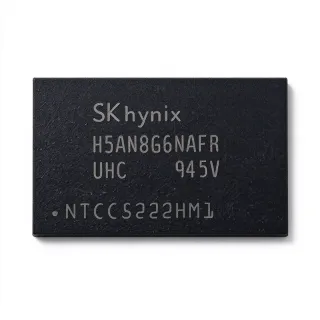
H5AN8G6NAFR-RDC - 8Gb DDR4 SDRAM 512Mx16 | SK Hynix
MPN: H5AN8G6NAFR-RDC ✓ Active| Qty | Unit Price | Extended |
|---|---|---|
| 1 | $4.2 | $4.20 |
| 10 | $3.9 | $39.00 |
| 100 | $3.55 | $355.00 |
| 500 | $3.3 | $1,650.00 |
| 1,000 | $3.05 | $3,050.00 |
H5AN8G6NAFR-RDC Overview
DDR4 SDRAM is the fourth generation of double-data-rate synchronous dynamic random-access memory, the dominant main-memory technology in servers, workstations, desktop PCs, and embedded systems. As a memory IC within the DRAM hierarchy, it synchronizes all operations to a clock and transfers data on both clock edges, doubling effective bandwidth versus SDR DRAM. DDR4 raised the bank-group architecture, lowered operating voltage from 1.5V (DDR3) to 1.2V, and increased prefetched data per access to 8n.
Key features of this device include 8Gb density in a single die, a 16-bit wide data bus, multi-bank page burst access mode, and DDR4 bank-group architecture that improves effective bandwidth at a given clock rate. The 1.2V core supply significantly reduces memory-subsystem power compared with DDR3 solutions, which matters in density-critical modules and battery-operated equipment.
Architecturally, the H5AN8G6NAFR family uses CMOS DRAM core technology with DDR4 signaling, on-die termination support, and a JEDEC-standard DDR4 interface. The -RDC speed grade suffix identifies the speed bin and temperature-range configuration of this variant; consult the SK Hynix datasheet for the exact clock-rate and timing parameters of the -RDC bin.
Typical applications include main memory for industrial PCs and embedded controllers, DRAM memory modules (SO-DIMM/DIMM component population), networking equipment buffers, and high-capacity storage caching systems. The x16 organization suits designs that need moderate bus widths with high per-device density.
Design consideration: DDR4 routing requires length-matched, impedance-controlled fly-by or tree topologies; verify the controller supports x16 devices and the -RDC speed grade before layout.
This page synthesizes datasheet data, distributor listings, and verified drop-in alternatives not consolidated in the manufacturer datasheet.
Drop-in alternatives for H5AN8G6NAFR-RDC — same package, pin-to-pin compatible. Different-package parts requiring PCB rework are excluded.
Variants in this series
Same-series models that are drop-in compatible with H5AN8G6NAFR-RDC (same form factor and footprint) — differing in Package, Interface, RoHS Status, Organization, Density.
Quick Comparison Tool — Select alternative parts for side-by-side comparison:
H5AN8G6NAFR-UHC
✅ Drop-In✓ In Stock
$5.7422 / Unit
View Datasheet →H5AN8G6NAFR-VKC
✅ Drop-In✓ In Stock
$6.25 / Unit
View Datasheet →H5AN8G6NAFR-PBC
✅ Drop-In ⚠️ Specs Unverified✓ In Stock
$3.55 / Unit
View Datasheet →H5AN8G8NAFR-RDC
✅ Drop-In ⚠️ Specs Unverified✓ In Stock
$2.95 / Unit
View Datasheet →MT40A512M16JY-075E
✅ Drop-In✓ In Stock
$30.5 / Unit
View Datasheet →H5AN8G6NAFR-RDC Maximum Ratings & Electrical Characteristics
| Memory Type | DDR4 SDRAM |
| Memory Density | 8 Gb |
| Organization | 512M x 16 |
| Supply Voltage | 1.2 V |
| Interface | DDR4 (JEDEC-standard) |
| Access Mode | Multi Bank Page Burst |
| Package Code | TFBGA |
| Package Shape | Rectangular |
| Number of Terminals | 96 |
| Mounting Type | Surface Mount |
| Temperature Grade | OTHER (per Partstack listing) |
| Technology | CMOS |
| RoHS Status | Compliant (Lead-Free & Halogen-Free) |
| Speed Grade | -RDC (see datasheet for bin timing) |
| Family | H5AN8G4NAFR-xxC / H5AN8G8NAFR-xxC / H5AN8G6NAFR-xxC |
H5AN8G6NAFR-RDC rectangular Pin Configuration Guide
Pin configuration for H5AN8G6NAFR-RDC (rectangular package). This digital IC includes GPIO, communication interfaces (UART, SPI, I2C), and power pins. Refer to the manufacturer datasheet for alternate pin functions and configuration options. Essential for embedded system design and PCB layout.

No detailed pinout data available for H5AN8G6NAFR-RDC.
Refer to the datasheet for full pin configuration.
Typical Applications
H5AN8G6NAFR-RDC is suitable for 6 applications: Embedded Industrial PC Main Memory, DRAM Memory Modules (DIMM/SO-DIMM), Networking Equipment Packet Buffering, Automotive and Rugged Embedded Systems, Test and Measurement Instrumentation, Storage Systems and Caching.
Embedded Industrial PC Main Memory
The H5AN8G6NAFR-RDC provides 8Gb of DDR4 main memory in a single 96-ball TFBGA component, which suits industrial PC motherboards and COM Express modules that need high density without a large component count. Its 512M x 16 organization pairs naturally with x16 DDR4 controllers in embedded chipsets, and the 1.2V supply keeps memory power within typical industrial thermal budgets. Mounted on the PCB directly rather than on a module, the device eliminates SO-DIMM connector cost and improves shock and vibration tolerance for factory automation and edge-compute deployments. Designers should follow SK Hynix's DDR4 routing guidance for fly-by command/address topology and length matching.
Recommended
DRAM Memory Modules (DIMM/SO-DIMM)
The H5AN8G6NAFR-xxC family is used as a component population on DDR4 DIMMs and SO-DIMMs, where 16 x8 or x16 devices build 8 GB to 16 GB capacities. According to the SK Hynix datasheet, the family targets main-memory applications requiring large density and high bandwidth - exactly the module use case. The multi-bank page burst access mode sustains the sequential and random bandwidth that module controllers expect, and the 1.2V operation aligns with the JEDEC DDR4 module power budget. x16 parts like this one enable lower-chip-count module designs for cost-sensitive and space-constrained SODIMM form factors.
Recommended
Networking Equipment Packet Buffering
Routers, switches, and network appliances use 8Gb x16 DDR4 components like the H5AN8G6NAFR-RDC as deep packet buffers and table memory behind traffic-processing ASICs. The device's multi-bank page burst architecture supports the high sequential bandwidth needed when draining packet bursts, while 8Gb on one component keeps the buffer subsystem compact on dense line cards. Its 1.2V operation reduces power on cards where every watt matters for airflow-limited chassis. The RoHS-compliant, lead-free and halogen-free construction also meets telecom environmental requirements for network equipment deployed in regulated markets.
Recommended
Automotive and Rugged Embedded Systems
Infotainment head units, gateways, and rugged controllers use 8Gb DDR4 components to host large operating-system images and frame buffers. The H5AN8G6NAFR-RDC's TFBGA-96 package provides a low-profile, solder-attached solution that withstands vibration better than socketed memory, and its 1.2V DDR4 interface integrates with automotive-grade SoCs that expose DDR4 controllers. Designers should confirm the -RDC temperature grade against their cabin or under-hood environment, or select an appropriate SK Hynix temperature-suffix variant within the same H5AN8G6NAFR-xxC family, since the package footprint is shared across the family.
Recommended
Test and Measurement Instrumentation
Oscilloscopes, logic analyzers, and protocol analyzers rely on deep capture memory to record long signal histories. The H5AN8G6NAFR-RDC's 8Gb density in a single component lets instrument designers build multi-gigabyte capture buffers with fewer parts, and its 512M x 16 organization supports the wide, high-throughput data paths between front-end acquisition ASICs and buffer memory. The multi-bank page burst access mode sustains sustained streaming write bandwidth during acquisition and read bandwidth during playback analysis. RoHS-compliant construction supports environmental regulations that commercial test equipment must meet in global markets.
Recommended
Storage Systems and Caching
SSD controllers and enterprise storage arrays use DDR4 DRAM as firmware memory, mapping tables, and write caches. The H5AN8G6NAFR-RDC offers 8Gb of cache memory in one 96-ball TFBGA component, allowing 2 GB of DRAM per four devices - enough for enterprise FTL tables on multi-terabyte SSDs. Its 1.2V supply keeps controller-board power within SSD thermal limits, and the compact rectangular package fits alongside NAND dies on constrained PCBs. The multi-bank page burst mode supports the small random read/write patterns typical of FTL table lookups during host I/O processing.
Recommended
Recommended Products Summary
Engineering reference data for H5AN8G6NAFR-RDC — comparison, design guidance, and compliance information.
Selection Guide
Comparison with Alternatives
| Parameter | This Product | H5AN8G6NAFR-UHC | H5AN8G6NAFR-VKC | H5AN8G6NAFR-PBC | H5AN8G8NAFR-RDC | MT40A512M16JY-075E |
|---|---|---|---|---|---|---|
| Package | TFBGA-96 | TFBGA-96 - same | TFBGA-96 - same | TFBGA-96 - same | TFBGA-96 - same | FBGA-96 - same footprint |
| Brand | SK Hynix | SK Hynix | SK Hynix | SK Hynix | SK Hynix | Micron Technology |
| Density | 8 Gb | 8 Gb | 8 Gb | 8 Gb | 8 Gb | 8 Gb |
| Organization | 512M x 16 | 512M x 16 | 512M x 16 | 512M x 16 | 1G x 8 | 512M x 16 |
| Supply Voltage | 1.2 V | 1.2 V | 1.2 V | 1.2 V | 1.2 V | 1.2 V |
| Memory Type | DDR4 SDRAM | DDR4 SDRAM | DDR4 SDRAM | DDR4 SDRAM | DDR4 SDRAM | DDR4 SDRAM |
| Speed Grade | -RDC | -UHC | -VKC (2400 Mbps class) | -PBC | -RDC | -075E (1875 Mbps class) |
Key Differentiators
- Native -RDC speed-bin qualification (vs H5AN8G6NAFR-UHC)
- x16 organization reduces component count (vs H5AN8G8NAFR-RDC)
- Second-source availability in the same footprint (vs MT40A512M16JY-075E)
Design Notes
DDR4 x16 designs with the H5AN8G6NAFR-RDC should use length-matched routing: keep DQ/DM/DQS trace skew within controller spec (typically +/-10 ps intra-byte), and route command/address in fly-by topology with VTT termination at the end of the chain. Maintain controlled impedance (40 ohm single-ended, 80 ohm differential for DQS pairs) and reference signals to solid ground planes. Follow the controller vendor's DDR4 layout guide in addition to the SK Hynix datasheet routing recommendations.
The device operates from a 1.2V VDD core; provide bulk capacitance (e.g., several 10 uF ceramics per device) plus 0.1 uF high-frequency decoupling at each VDD ball pair, and a separate VTT rail terminated per the DDR4 termination spec for address/control lines. Verify power-up sequencing per the SK Hynix datasheet before releasing the memory controller reset - DDR4 initialization must complete before any command is issued or the state machine may lock up.
The -RDC suffix encodes the speed bin; do not assume it matches -UHC or -VKC timing tables. If substituting H5AN8G6NAFR-UHC/VKC/PBC or Micron MT40A512M16JY-075E, re-run memory training/calibration on the target board and confirm the controller supports the new bin's data rate. Also note H5AN8G8NAFR-RDC is x8 organization - it shares the package footprint but not the bus width, so controller configuration must change.
Compliance Information
Datasheet description states Lead-Free & Halogen-Free (RoHS Compliant). REACH and conflict-minerals declarations not stated in provided data.