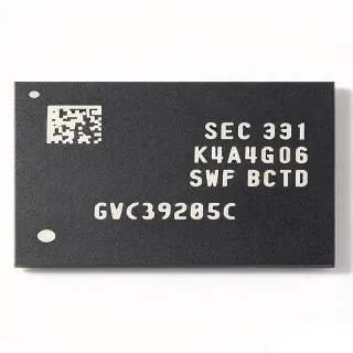
H5AN8G6NAFR-VKC - 8Gb DDR4 SDRAM 512Mx16 1.2V | SK Hynix
MPN: H5AN8G6NAFR-VKC ✓ Active| Qty | Unit Price | Extended |
|---|---|---|
| 1 | $8.01 | $8.01 |
| 10 | $7.55 | $75.50 |
| 100 | $7.05 | $705.00 |
| 500 | $6.65 | $3,325.00 |
| 1,000 | $6.25 | $6,250.00 |
H5AN8G6NAFR-VKC Overview
DDR4 SDRAM is the fourth generation of double-data-rate synchronous dynamic random-access memory, the dominant main-memory technology in PCs, servers, and embedded systems. In the memory hierarchy, DDR4 SDRAM sits above cache memories (SRAM) as main system memory, offering high density at low cost per bit, and transfers data on both rising and falling clock edges for bandwidth of several gigabytes per second per device.
Key features of the H5AN8G6NAFR-VKC include its 8Gb (gigabit) density in a single x16 organization, a 1.2V core supply that reduces power versus DDR3's 1.5V, and the compact FBGA-96 ball-grid package that simplifies high-density PCB routing. The -VKC speed grade code denotes DDR4-2666 class timing in SK Hynix's naming convention, supporting mainstream embedded and industrial memory designs. The part is specified as Lead-Free and Halogen-Free and is RoHS compliant per the manufacturer datasheet.
Architecturally, the device uses CMOS DRAM core technology with internal banks, burst-oriented operation, and standard DDR4 signaling (open-drain DQS strobes, on-die termination support, and JEDEC-standard command set). x16 organization means two data bytes per access, which suits designs using fewer memory chips and 16-bit or 32-bit wide memory buses, common in embedded controllers, networking appliances, and graphics/display buffers.
Typical applications include industrial PC and embedded controller main memory, SSD controller write buffers, networking and communication equipment line-card buffers, and set-top-box or smart-TV system memory where 1 GB per chip reduces component count.
Design consideration: DDR4 fly-by routing requires careful length matching of CK/CA signals, per-byte DQS termination, and VTT termination power design; verify controller timing versus the -VKC speed bin datasheet AC tables before layout.
This page synthesizes distributor pricing, drop-in alternatives, and practical design notes not found in the manufacturer datasheet.
Drop-in alternatives for H5AN8G6NAFR-VKC — same package, pin-to-pin compatible. Different-package parts requiring PCB rework are excluded.
Variants in this series
Same-series models that are drop-in compatible with H5AN8G6NAFR-VKC (same form factor and footprint) — differing in Package, Data Rate, Interface, Organization, RoHS Status.
Quick Comparison Tool — Select alternative parts for side-by-side comparison:
H5AN8G6NAFR-UHC
✅ Drop-In✓ In Stock
$5.7422 / Unit
View Datasheet →H5AN8G6NAFR-RDC
✅ Drop-In✓ In Stock
$3.05 / Unit
View Datasheet →H5AN8G6NAFR-PBC
✅ Drop-In✓ In Stock
$3.55 / Unit
View Datasheet →H5AN8G6NCJR-VKC
✅ Drop-In✓ In Stock
$60 / Unit
View Datasheet →MT40A512M16JY-075E
✅ Drop-In✓ In Stock
$30.5 / Unit
View Datasheet →H5AN8G6NAFR-VKC Maximum Ratings & Electrical Characteristics
| Memory Type | DDR4 SDRAM |
| Density | 8 Gb |
| Organization | 512M x 16 |
| Core Supply Voltage | 1.2 V |
| Technology | CMOS |
| Package | FBGA-96 (PBGA96) |
| Speed Grade | -VKC (DDR4-2666 class, per SK Hynix part numbering) |
| Data Rate Class | Up to 2666 MT/s (per -VKC speed code) |
| Family | H5AN8G4NAFR / H5AN8G8NAFR / H5AN8G6NAFR |
| Mounting Type | Surface Mount (BGA) |
| RoHS Status | Lead-Free & Halogen-Free, RoHS Compliant |
| Application | Main memory (high density, high bandwidth) |
H5AN8G6NAFR-VKC fbga-96 (pbga96) Pin Configuration Guide
Pin configuration for H5AN8G6NAFR-VKC (fbga-96 (pbga96) package). This digital IC includes GPIO, communication interfaces (UART, SPI, I2C), and power pins. Refer to the manufacturer datasheet for alternate pin functions and configuration options. Essential for embedded system design and PCB layout.

No detailed pinout data available for H5AN8G6NAFR-VKC.
Refer to the datasheet for full pin configuration.
Typical Applications
H5AN8G6NAFR-VKC is suitable for 6 applications: Embedded Controller Main Memory, SSD Controller Write Buffer, Networking and Communication Equipment, Smart TV and Set-Top-Box System Memory, Test and Measurement Instrumentation, Automotive Infotainment and Display Units.
Embedded Controller Main Memory
The H5AN8G6NAFR-VKC provides 1 GB of main memory in a single FBGA-96 package, making it ideal for industrial embedded controllers, edge gateways, and single-board computers that use 16-bit or 32-bit DDR4 memory buses. Its 8 Gb density at 1.2 V core voltage delivers DDR4 bandwidth and power efficiency versus DDR3 alternatives, and the x16 organization minimizes component count on compact boards. Designers typically place the SDRAM close to the CPU with fly-by clock/command routing, 40-ohm on-die termination settings, and per-byte DQS length matching within +/-25 mils. The -VKC speed bin supports DDR4-2666-class operation for mainstream embedded SoCs.
Recommended
SSD Controller Write Buffer
SSD controllers use DRAM to store FTL (flash translation layer) mapping tables; the H5AN8G6NAFR-VKC's 8 Gb (1 GB) capacity maps roughly 1 TB of NAND with standard 4 KB page mapping, all within one x16 device. The DDR4-2666-class interface provides over 4 GB/s peak bandwidth on a 16-bit bus, keeping map-table reads off the NAND bus during host I/O. Its 1.2 V operation and FBGA-96 footprint fit standard M.2 and U.2 controller reference designs, which commonly specify x16 DDR4 in this package. Power-loss protection circuits should hold CKE and CK low during brownout to avoid map corruption.
Recommended
Networking and Communication Equipment
Line cards, switches, and router control planes require deep packet buffering and large routing-table memory; the H5AN8G6NAFR-VKC offers 1 GB per device with 4+ GB/s peak bandwidth, suiting NPU/CPU companion memory in 1G/10G networking hardware. The 512M x 16 organization allows a 32-bit bus with just two chips, conserving board area on dense line cards, while the 1.2 V rail integrates with standard DDR4 VDDQ/VTT power trees. Thermal design should assume approximately 0.5-1 W per device under sustained traffic, verified with airflow modeling. -VKC bin timing tables must be programmed into the switch SoC's DDR4 training firmware.
Recommended
Smart TV and Set-Top-Box System Memory
High-definition set-top boxes and smart TVs use 1-2 GB of DDR4 for video frame buffers, OS execution, and graphics; one H5AN8G6NAFR-VKC provides the full gigabyte in a single 96-ball package, reducing BOM cost versus multiple smaller devices. The x16 bus matches mainstream SoC memory controllers, and the 1.2 V DDR4 interface keeps system idle power low for energy-star compliance. The -VKC DDR4-2666-class speed supports 4K video decode pipelines that stream multiple frame buffers concurrently. Consumer designs typically pair the SDRAM with a passive VTT termination network and use the SoC's hardware training for ZQ calibration.
Recommended
Test and Measurement Instrumentation
Oscilloscopes, logic analyzers, and signal generators require deep acquisition memory; the H5AN8G6NAFR-VKC supplies 1 GB per chip at DDR4 bandwidth for storing long capture records and processed waveform data. Its deterministic JEDEC-standard DDR4 command set integrates with FPGA memory controllers (Xilinx/Intel MIG designs commonly target x16 DDR4 in FBGA-96), and the 1.2 V rail simplifies bench-instrument power budgets. Designers must budget refresh (tRFC) interruptions into capture-continuous schemes, or buffer through FIFOs during refresh windows. Second-sourcing with Micron MT40A512M16JY-075E protects instrument production against DRAM allocation cycles.
Recommended
Automotive Infotainment and Display Units
Automotive head units and digital cockpit displays use 1-2 GB of DDR4 for navigation rendering, media playback, and instrument-cluster graphics; the H5AN8G6NAFR-VKC's single-chip gigabyte density and compact FBGA-96 package fit constrained dashboard electronics. The 1.2 V core reduces total memory-subsystem power, important for thermal management behind windshields where ambient temperatures are elevated. Note: for AEC-Q100-qualified positions, verify the automotive grade suffix requirements with SK Hynix, since standard -VKC parts may not carry automotive qualification - the -VKIR/-UHCR automotive variants in the SK Hynix DDR4 lineup exist for that purpose. Layout should follow fly-by routing with controlled impedance.
Recommended
Recommended Products Summary
Engineering reference data for H5AN8G6NAFR-VKC — comparison, design guidance, and compliance information.
Selection Guide
Comparison with Alternatives
| Parameter | This Product | H5AN8G6NAFR-UHC | H5AN8G6NAFR-RDC | H5AN8G6NAFR-PBC | H5AN8G6NCJR-VKC | MT40A512M16JY-075E |
|---|---|---|---|---|---|---|
| Package | FBGA-96 (PBGA96) | FBGA-96 - same | FBGA-96 - same | FBGA-96 - same | FBGA-96 - same | FBGA-96 - same |
| Brand | SK Hynix | SK Hynix | SK Hynix | SK Hynix | SK Hynix | Micron Technology |
| Density | 8 Gb | 8 Gb | 8 Gb | 8 Gb | 8 Gb | 8 Gb |
| Organization | 512M x 16 | 512M x 16 | 512M x 16 | 512M x 16 | 512M x 16 | 512M x 16 |
| Core Voltage | 1.2 V | 1.2 V | 1.2 V | 1.2 V | 1.2 V | 1.2 V |
| Speed Grade | -VKC (DDR4-2666 class) | -UHC (different bin) | -RDC (lower bin) | -PBC (lower bin) | -VKC (same class) | -075E (DDR4-2666 class) |
| RoHS / Lead-Free | Compliant / Lead-Free & Halogen-Free | Compliant | Compliant | Compliant | Compliant | Compliant |
Key Differentiators
- Top speed bin within the 8Gb x16 NAFR family (vs H5AN8G6NAFR-RDC)
- Identical footprint second-sourcing from SK Hynix bins (vs H5AN8G6NAFR-UHC)
- Dual-vendor drop-in capability (vs MT40A512M16JY-075E)
Design Notes
DDR4 fly-by topology: route CK/CK# and command/address signals in a daisy chain from the controller through the SDRAM with on-die termination (ODT) enabled, and length-match DQ/DM/DQS per byte lane within +/-25 mils (estimated typical DDR4 layout rule). Keep CK/CK# as a tightly coupled differential pair (100-ohm differential impedance) and reference all signals to solid VSS/VDD planes. The FBGA-96 ballout places DQ byte lanes on opposite sides, so plan the controller-to-chip escape routing before placing decoupling capacitors.
Power the H5AN8G6NAFR-VKC from a 1.2 V VDD rail with tight tolerance (per DDR4 standard, typically +/- 3%) and provide a separate VTT termination rail equal to VDD/2 with a sink-source LDO or switching VTT regulator. Estimate: at DDR4-2666 with moderate utilization, per-device current commonly falls in the 300-600 mA range - size the VTT rail for the sum of all termination loads. Place one 100 nF ceramic per VDD ball pair plus bulk 10 uF near the package; follow the vendor reference design capacitor map for ball-level placement.
Three frequent pitfalls: (1) substituting speed bins without updating controller timing registers - the -VKC, -UHC, and -RDC bins have different tCK/CL/tRCD/tRP tables, so firmware must be re-trained per bin; (2) ignoring tRFC refresh time in bandwidth-critical designs, which causes periodic throughput dips; (3) verifying temperature limits only against ambient - confirm the datasheet operating range for the -VKC bin and derate for enclosure heating. Also confirm genuine sourcing: DDR4 is heavily counterfeited; buy from LCSC/authorized channels and verify date codes.
Compliance Information
Datasheet states: 8Gb DDR4 SDRAM Lead-Free & Halogen-Free (RoHS Compliant). REACH and conflict-minerals declarations not stated in provided data - request from SK Hynix.