Memory ICs
Subcategories
Products (459)

MT40A1G8AG-062E - 8Gb DDR4 SDRAM 3200Mb/s x8 | Micron
The Micron MT40A1G8AG-062E AUT:R is an 8Gbit DDR4 SDRAM DRAM organized as 1G x 8, operating at 1.6 GHz (DDR4-3200 data rate) with a 19 ns cycle time, housed in a 78-ball FBGA package measuring 7.5 x 11 mm. It runs from a 1.2V VDD supply and is qualified for the automotive temperature range (AUT suffix). DDR4 SDRAM (Double Data Rate 4 Synchronous Dynamic Random Access Memory) is the fourth generation of the DDR DRAM family, succeeding DDR3. In the memory hierarchy it sits within the broader categories of DRAM, semiconductor memory, and memory ICs. DDR4 introduced a lower core voltage (1.2V vs 1.35/1.5V for DDR3), bank groups, and higher data rates up to 3200 MT/s, making it the dominant main-memory technology for servers, workstations, and embedded processors of its generation. Key features of this part include the 8Gbit density in a space-saving x8 organization, DDR4-3200 speed grade (-062E timing suffix corresponding to a 19 ns clock cycle), 1.2V low-voltage operation that reduces memory subsystem power versus DDR3, and automotive-grade screening for extended operating environments. The 78-ball FBGA (7.5 x 11 mm) fine-pitch ball grid array is the industry-standard footprint for x8 DDR4 components, which supports second-source layouts. Architecturally, the device uses the DDR4 bank-group structure (four groups of four banks), 8n prefetch, and on-die termination (ODT) to sustain high bus efficiency. Command/address parity (CA parity) and alert output features improve system reliability in mission-critical platforms, attributes that matter in automotive and industrial designs where the AUT grade targets. Typical applications include automotive infotainment and ADAS main memory alongside processors and SoCs, industrial automation controllers and gateways, and networking/telecom line-card memory buffers. The x8 organization suits designs using discrete DRAM chips soldered directly on the CPU board or on memory risers. Design consideration: DDR4 signal integrity requires length-matched, fly-by routed command/address trees, per-byte ODT tuning via Mode Registers, and VTT termination supplied by a dedicated termination regulator; verify the SoC memory controller supports DDR4-3200 timing (tCK = 0.625 ns nominal). This page synthesizes distributor pricing, drop-in alternatives, and practical design notes not found in the manufacturer datasheet.
MT40A1G8SA-062E - 8Gb DDR4 SDRAM 3200MT/s | Micron
The Micron MT40A1G8SA-062E is an 8Gb DDR4 SDRAM organized as 1G x 8, operating at a data rate of 3200 MT/s (DDR4-3200) with a 1.6 GHz clock, housed in a 78-ball FBGA package (7.5x11 mm) and powered from a 1.2V supply (VDD = VDDQ = 1.2V +/-60mV) with a separate 2.5V VPP supply. DDR4 SDRAM (Double Data Rate 4 Synchronous Dynamic Random-Access Memory) is a type of volatile memory that transfers data on both edges of the clock, doubling the data rate per clock cycle. Within the memory hierarchy, it sits as main system memory below CPU caches and above storage. DDR4 operates at 1.2V core voltage versus DDR3's 1.5V, cutting memory subsystem power by roughly 20%, and introduced bank groups, on-die termination refinements, and higher pre-fetch-efficient signaling for mainstream servers, workstations, and embedded controllers. Key features include on-die, internal, adjustable VREFDQ generation, which removes the need to route an external reference voltage and improves noise margins; 1.2V pseudo open-drain I/O for cleaner eye diagrams at 3200 MT/s; and 16 internal banks arranged as 4 bank groups of 4 banks, enabling faster random row access through bank-group interleaving. The device supports temperature-dependent refresh with 8192-cycle refresh: 64ms at -40C to +85C, 32ms above +85C to +95C, and 16ms above +95C, preserving data integrity across the industrial temperature range. Additional features include auto self-refresh, write leveling, dynamic on-chip termination (ODT), CRC function, auto precharge, and ZQ calibration. The CAS latency is CL22 at DDR4-3200 with burst lengths of 8 and 4 (burst chop), and the row access time is approximately 19 ns. Typical applications include server and data center DIMM modules, networking equipment line-card memory, industrial embedded controllers, and high-performance computing systems that require high bandwidth and large capacity per device. The x8 organization suits both ECC-based module designs and discrete solder-down memory footprints. When designing with this device, provide a stable 1.2V VDD/VDDQ rail and a 2.5V VPP rail for wordline boost, decouple all supply balls closely, and follow DDR4 fly-by routing and length-matching guidelines to maintain signal integrity at 3200 MT/s. This page adds value beyond the datasheet by synthesizing distributor pricing, same-footprint drop-in alternatives across Micron, Samsung, and SK Hynix, and practical design notes for DDR4 layout and power sequencing.
MT40A1G8WE-083E - 8Gb DDR4 SDRAM 2400 | Micron Technology
The Micron Technology MT40A1G8WE-083E is an 8Gb (1Gb x 8) automotive-grade DDR4 SDRAM operating at DDR4-2400 (1.2 GHz clock data rate) from a 1.2V VDD/VDDQ supply, housed in a 78-ball FBGA (8 x 12 mm) package with a -40C to +95C operating range. DDR4 SDRAM (Double Data Rate 4 Synchronous Dynamic Random Access Memory) is the fourth generation of DDR memory, sitting in the system hierarchy as main-memory DRAM beneath the processor cache. It transfers data on both clock edges, doubling effective bandwidth versus SDR memory, and organizes storage into multiple internal banks that can be activated, read, and precharged in interleaved fashion to sustain high throughput. Key features include 16 internal banks in 4 groups of 4 (x8 configuration), an 8n-bit prefetch architecture, on-die internal adjustable VREFDQ generation, and a 1.2V pseudo open-drain I/O interface. VDD = VDDQ = 1.2V with a tolerance of plus/minus 60mV, while VPP = 2.5V (-125mV, +250mV) supplies the DRAM cell array. Programmable data strobe preambles, data strobe preamble training, and command/address latency (CAL) support robust high-speed signaling. The part implements temperature-aware refresh: an 8192-cycle refresh at a 64ms interval for -40C to +85C, 32ms above 85C to 95C, and reduced intervals beyond that, preserving data integrity across the full automotive temperature range. The -083E speed grade corresponds to the industry DDR4-2400 bin, delivering 2400 MT/s per data pin, or 19.2 Gb/s aggregate bandwidth on the x8 interface. Typical applications include automotive ADAS domain controllers, telematics and infotainment units, industrial networking equipment, and test-and-measurement systems where wide-temperature DRAM is required. The WE (wide-temperature) suffix and -IT automotive screening make it suitable for designs targeting AEC-aligned qualification flows. Design consideration: the 78-ball FBGA requires controlled-impedance fly-by routing on the command/address bus and length-matched data strobe pairs; follow Micron's DDR4 point-to-point layout guidelines and enable write leveling in the memory controller. This page synthesizes distributor pricing, verified speed-grade alternatives, and design guidance not found in the manufacturer datasheet alone.
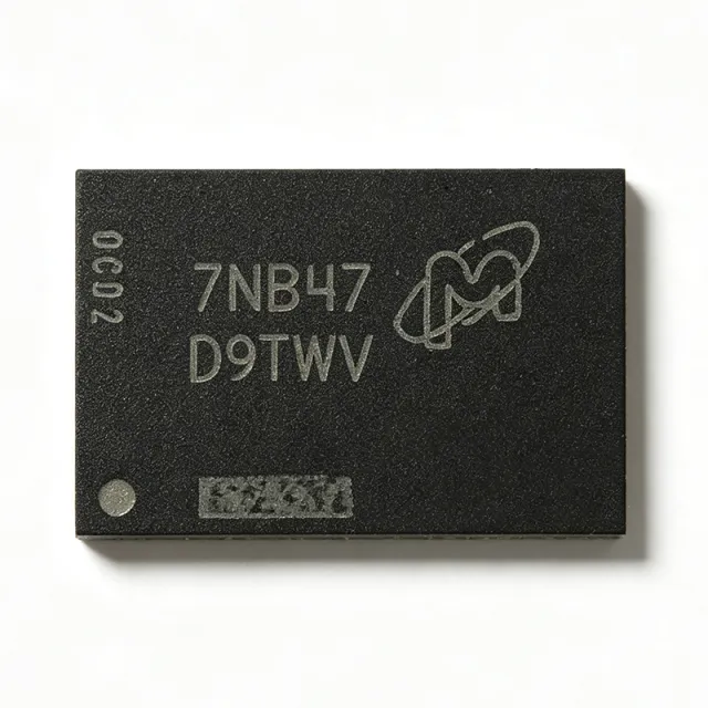
MT40A256M16GE-075E:B - 4Gb DDR4 SDRAM 2666 MT/s | Micron
The Micron MT40A256M16GE-075E:B is a 4Gbit DDR4 SDRAM memory IC organized as 256M x 16, operating at a data rate of 2666 MT/s (industry speed grade DDR4-2666, 1.33 GHz clock domain) with VDD = VDDQ = 1.2V +/-60mV, housed in a 96-ball FBGA (9 x 14 mm) package. DDR4 SDRAM (Double Data Rate 4 Synchronous Dynamic Random Access Memory) is the fourth generation of the DDR DRAM family, sitting within the hierarchy: DRAM -> SDRAM -> DDR SDRAM -> DDR4 -> volatile memory IC. DDR4 doubles the bank count and lowers the operating voltage relative to DDR3, improving bandwidth and power efficiency in computing, networking, and embedded systems. The JEDEC-defined DDR4 interface uses a pseudo open-drain I/O at 1.2V, along with on-die termination and adjustable internal VREFDQ generation to maintain signal integrity at high data rates. Key features of this device include 16 internal banks, temperature-controlled refresh (TCR) that extends refresh interval automatically up to 95C, and both 64ms/8192-cycle refresh (at <=85C per JEDEC convention) and 32ms/8192-cycle refresh modes. The 1.2V pseudo open-drain I/O reduces I/O power compared to DDR3L, and on-die internal adjustable VREFDQ generation eliminates the need for external reference voltage routing on the PCB. Architecturally, the die uses 256Mbit x16 organization with DDR4's bank-group structure, supporting burst lengths of 8 with sequential and interleaved options, and commands are registered on both clock edges to achieve the 2666 MT/s rate. VPP core supply is 2.5V (-125mV/+250mV) per Micron datasheet documentation. Typical applications include FPGA and processor memory subsystems (such as AMD Zynq UltraScale+ MPSoC designs), networking line cards, industrial controllers, and embedded computing modules requiring a 16-bit-wide DDR4 interface. Design consideration: verify the memory controller's supported speed grades and the -075E (2666 MT/s) timing set against your clock plan; derate to DDR4-2133 or DDR4-2400 operating points if board topology limits signal integrity. This page synthesizes distributor pricing, drop-in same-package alternatives, lifecycle notes, and practical design guidance not found in the manufacturer datasheet. Price references are as of 2026-09-03.

MT40A256M16LY-062E - 4Gb DDR4 SDRAM x16 | Micron
The Micron MT40A256M16LY-062E is a 4Gbit DDR4 SDRAM memory IC organized as 256M x16, operating at a 1.6 GHz clock (DDR4-2666 class) with a 19 ns column access latency, housed in a 96-ball FBGA package measuring 7.5 x 13.5 mm. DDR4 SDRAM (Double Data Rate 4 Synchronous Dynamic Random Access Memory) is the fourth generation of the JEDEC DDR memory family. A DRAM stores each bit in a capacitor within an integrated circuit, requiring periodic refresh, and its synchronous interface means all operations are timed to a clock signal. In the memory hierarchy, this component sits within DRAM components -> DDR4 SDRAM -> SDRAM -> volatile memory, and serves as the primary working memory for processors and SoCs. Key features of the MT40A256M16LY-062E include the x16 organization preferred for lower pin-count controllers, auto self-refresh, auto precharge, write leveling, CRC, data mask (DM), dynamic on-chip termination (ODT), and ZQ calibration. The -062E speed grade corresponds to a 19 ns tAA (CL19 at DDR4-2666), and the device operates from a 1.2V core supply, delivering roughly 20 percent lower power than DDR3 at the same data rate. Architecturally, the device implements the DDR4 bank-group structure, which interleaves precharge and activate operations across four bank groups to raise effective bandwidth without increasing core frequency. The x16 interface uses a 16-bit data path with differential data strobes (UDQS/LDQS) and per-byte data mask, and CRC protects command/address integrity on the CA bus for improved signal integrity at high speeds. Typical applications include embedded processor main memory, industrial controllers, networking equipment, and automotive/industrial-grade systems (the AUT and IT temperature variants cover -40C to +95C). The 96-FBGA footprint is a de facto standard that multiple DRAM vendors share. Design consideration: maintain fly-by termination topology for the command/address bus and follow Micron's published routing guidelines for length matching of DQ/DSQS; x16 parts use one ODT value per byte, so program ODT carefully in mixed-width memory subsystems. This page synthesizes distributor pricing, drop-in alternatives from multiple DRAM vendors, and practical design notes not found in the Micron datasheet alone.
MT40A2G8AG-062E - 16Gb DDR4 SDRAM 2Gx8 3200Mbps | Micron
The Micron Technology MT40A2G8AG-062E is a 16Gb DDR4 SDRAM organized as 2G x 8, operating at 1.2V (POD12) with a data rate of 3200 MT/s (1600 MHz clock, CL=22/19 ns access time) in a 78-ball FBGA (7.5 x 11 mm) package. DDR4 SDRAM is the fourth generation of double-data-rate synchronous dynamic random-access memory, an evolution of DDR3 that lowers operating voltage to 1.2V, doubles bank groups to eight banks per group, and adds features such as Bank Group Architecture, DBI (data bus inversion), CA parity, and VPP (2.5V wordline boost supply). In the memory hierarchy, this component sits as a discrete DRAM die used to populate server DIMMs, memory-down embedded designs, and networking line cards, forming the main-memory tier below CPU caches in a computer or embedded system. Key features include 16Gbit density in a single die, x8 organization with eight internal banks, DDR4-3200 speed grade (-062E means tCK = 0.625 ns), POD12 I/O interface for lower switching power, and on-die termination (ODT). The AG die revision is the current-generation product replacing the earlier SA-die MT40A2G8SA variants, offering improved refresh and reliability parameters. The device uses Micron's advanced DRAM process with 8n-bank, four bank-group architecture, enabling high sustained bandwidth. It supports activation-to-activation command spacing (tRRD_S/tRRD_L), write CRC for data integrity, and programmable CAS latency up to CL22. Operating temperature ranges vary by suffix: AUT (automotive), AIT (industrial), and AAT (automotive application) grades are available, with commercial -062E:F variants for standard use. Typical applications include embedded systems, networking and telecom equipment, industrial controllers, server memory modules, and consumer electronics that require high-bandwidth main memory in a memory-down configuration. Design considerations: DDR4 routing requires length-matched, impedance-controlled fly-by or point-to-point topology; the POD12 interface requires VDDQ = 1.2V and VPP = 2.5V supplies with proper decoupling. Follow Micron's DDR4 layout guidelines for address/command tree routing and ODT calibration (ZQ pin). This page synthesizes distributor pricing, drop-in alternatives including the Alliance Memory second-source, and practical design notes not found in the manufacturer datasheet. Prices as of 2026-09-04.
MT40A2G8JE-062E AAT:E - 16Gb DDR4-3200 Automotive SDRAM | Micron
The Micron Technology MT40A2G8JE-062E AAT:E is a 16Gbit automotive-grade DDR4 SDRAM organized as 2G x 8, operating at DDR4-3200 (1600 MHz clock, PC4-25600) from a 1.2V VDD/VDDQ supply, housed in a 78-ball FBGA (9 x 11 mm) package rated from -40C to +105C. DDR4 SDRAM (Double Data Rate 4 Synchronous Dynamic Random Access Memory) is the fourth generation of JEDEC-defined DDR DRAM, sitting within the memory IC hierarchy under DRAM components. Compared with DDR3, DDR4 halves the interface voltage to 1.2V, doubles the internal bank count (16 banks in 4 groups for x8), and adds features such as on-die internal adjustable VREFDQ generation, bank-group architecture, and tighter command signaling, enabling higher data rates with lower power per transfer. Key features of this device include the 16Gbit single-die density in a x8 organization, DDR4-3200 speed grade (-062E, 19 ns access time), 1.2V pseudo open-drain I/O, and a VPP supply of 1.2V (tolerance -125 mV/+250 mV per datasheet). The AAT automotive temperature rating (-40C to +105C) and Micron's automotive qualification make it suitable for under-hood-adjacent and high-reliability environments. The refresh interval extends at the extended temperature range, and internal refresh management simplifies controller integration. Technically, the Z32D die uses 16 internal banks (x8: 4 groups of 4) with bank-group interleaving that sustains DDR4-3200 throughput while keeping row-activation overhead bounded. On-die, internal, adjustable VREFDQ generation removes the need for an external reference voltage rail on the DQ byte, reducing BOM count and board-layer requirements. POD12 (1.2V pseudo open-drain) signaling reduces termination power versus DDR3. Typical applications include automotive ADAS image-processing and sensor-fusion platforms, telematics and gateway modules, industrial gateways and edge-compute controllers, and networking line-card buffering where 16Gbit density, x8 width, and AEC-oriented quality are required. Design consideration: at DDR4-3200, fly-by command/address routing with per-DQ-byte length matching and VTT termination is essential; verify controller drive strength and ODT settings against the Micron datasheet IBIS models before tape-out. This page synthesizes distributor pricing, drop-in alternatives (including the Alliance Memory second source), and practical design notes not consolidated in the manufacturer datasheet. Pricing references are as of 2026-09-02.
MT40A512M16AD-062E - 8Gbit DDR4 SDRAM x16 3200MT/s | Micron
The Micron Technology MT40A512M16AD-062E AUT:E is an 8 Gbit DDR4 SDRAM organized as 512M x16, operating at a clock rate of 1.6 GHz (data rate up to 3200 MT/s) with a 19 ns row cycle time, housed in a 96-ball FBGA (TFBGA) package measuring 7.5 mm x 13.5 mm. DDR4 SDRAM (Double Data Rate 4 Synchronous Dynamic Random Access Memory) is the fourth generation of the JEDEC DDR memory family used as main memory in computing and embedded systems. Compared with DDR3, DDR4 lowers core supply voltage, increases bank groups, and raises maximum data rates. In the memory hierarchy it sits as DRAM component -> DDR SDRAM -> synchronous DRAM -> semiconductor memory, bridging the gap between nonvolatile storage and processor caches. Key features of this part include the x16 data-width organization that allows single-component designs in embedded processors and FPGAs, the -062E speed grade supporting 3200 MT/s operation, and the automotive-qualified AUT:E variant family from Micron. The POD (pseudo-open drain) I/O interface reduces I/O power at high data rates, and programmable data strobe preambles improve signal integrity at speed. Technically, the device uses an 8n prefetch architecture with bank groups, on-die termination (ODT), and DLL-based timing. The x16 configuration uses a single DQS strobe pair with DM mask support, simplifying controller interface for medium-bandwidth systems. Ball-map and JEDEC-standard DDR4 x16 ballout enable reuse of reference layouts. Typical applications include automotive infotainment and ADAS memory buffers, industrial human-machine interfaces, networking line cards, and FPGA-based vision and data-acquisition systems requiring 1 GB per component of high-bandwidth volatile memory. Design consideration: DDR4 routing requires length-matched fly-by command/address lines and careful VTT termination; verify the controller supports 3200 MT/s or derate the speed grade selection accordingly. This page synthesizes distributor pricing, drop-in alternatives, and practical design notes not found in the manufacturer datasheet.
MT40A512M16JY-083E - 8Gb DDR4 SDRAM 2400MT/s x16 | Micron
The Micron Technology MT40A512M16JY-083E is an automotive-grade 8Gb DDR4 SDRAM organized as 512M x16, operating at a 1.2 GHz clock (DDR4-2400 class) in a 96-ball FBGA (8x14 mm) package. It runs from VDD = VDDQ = 1.2V +/-60mV with a separate VPP of 2.5V (-125mV/+250mV) for the word-line charge pump. DDR4 SDRAM (Double Data Rate fourth-generation synchronous dynamic random-access memory) is the dominant main-memory technology for embedded processors, industrial controllers, and automotive computing platforms. Within the memory hierarchy it sits below cache (SRAM) and above storage (NAND flash), providing high-bandwidth, low-cost-per-bit working memory. The x16 organization suits processors with 16-bit or 32-bit memory controllers. Key features include the -083E speed grade (tCK = 0.83 ns, 1.2 GHz clock, 2400 MT/s data rate), on-die internal adjustable VREFDQ generation that eliminates external reference resistors, and a 1.2V pseudo open-drain I/O structure that lowers I/O power versus DDR3. Automotive qualification targets the extended temperature range demanded by in-vehicle applications. Architecturally, the device uses an 8-bank DDR4 core with bank-group burst access, 8n prefetch, and programmable CAS latency. Refresh is 8192-cycle per refresh window: 64ms at TC of -40C to 85C, 32ms above 85C to 95C, and 16ms above 95C, enabling reliable operation in hot automotive cabins. Typical applications include automotive ADAS and infotainment main memory, industrial HMI and edge-AI platforms, networking line-card buffers, and test-and-measurement systems. Design consideration: honor the separate 2.5V VPP rail in your power tree; omitting it or tying it to 1.2V prevents proper word-line biasing and can prevent boot. Follow Micron's DDR4 layout guidelines for fly-by routing with on-die termination. This page synthesizes distributor pricing, drop-in alternatives, and practical design notes not found in the manufacturer datasheet.
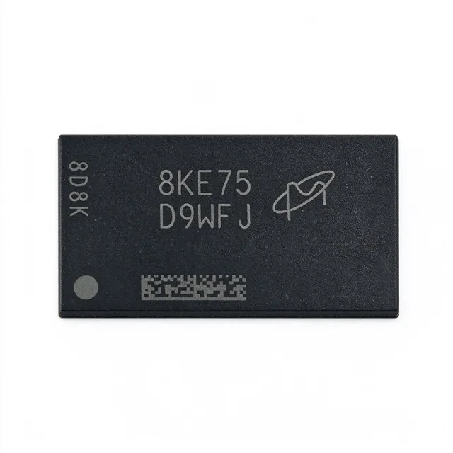
MT40A512M16LY-062E - 8Gb DDR4 SDRAM 3200MT/s | Micron
The Micron Technology MT40A512M16LY-062E is an 8Gb DDR4 SDRAM organized as 512M x 16, operating at the DDR4-3200 speed grade (1.6 GHz clock, 3200 MT/s data rate) in a 96-ball FBGA package measuring 7.5 x 13.5 mm. DDR4 SDRAM (fourth-generation Double Data Rate Synchronous Dynamic Random-Access Memory) is a volatile memory that transfers data on both edges of the clock, doubling effective data rate versus SDR DRAM. Within the memory hierarchy it sits as the main-system-memory class of DRAM, below caches and above storage, and succeeds DDR3 with lower operating voltage and higher densities. DDR4 runs its core and I/O at VDD = VDDQ = 1.2V +/- 60mV, down from DDR3's 1.5V, cutting dynamic power while enabling higher speeds and per-device capacity up to 16Gb. Key features of this device include 16 internal banks grouped in 2 bank groups of 4 (x16 configuration), on-die internal adjustable VREFDQ generation that simplifies memory-controller design, and 1.2V pseudo open-drain I/O. The IT industrial temperature grade supports a refresh window of 8192 cycles at 64ms for -40C to +85C, 32ms for >85C to +95C, and 16ms beyond 95C. VPP is supplied at 2.5V (-125mV/+250mV) exclusively for cell bootstrap pumping. Advanced capability set includes auto self-refresh, write leveling, dynamic on-chip termination (ODT), CRC and CA parity support, data mask, auto precharge, asynchronous reset, and ZQ calibration via an external 240-ohm reference resistor. Typical applications are industrial embedded controllers, networking equipment line cards, and high-performance computing or data-center memory subsystems where 3200 MT/s bandwidth per device and industrial temperature range are required. Design-wise, plan controlled-impedance fly-by routing, 1.2V and 2.5V rails with adequate decoupling, and connect the ZQ ball to ground through exactly 240 ohms; the controller must support 2tCK ODT updates at this speed grade. This page adds distributor pricing tiers, drop-in alternatives across Micron, Nanya, Samsung, and SK hynix, plus practical DDR4 design notes not found in the manufacturer datasheet alone.
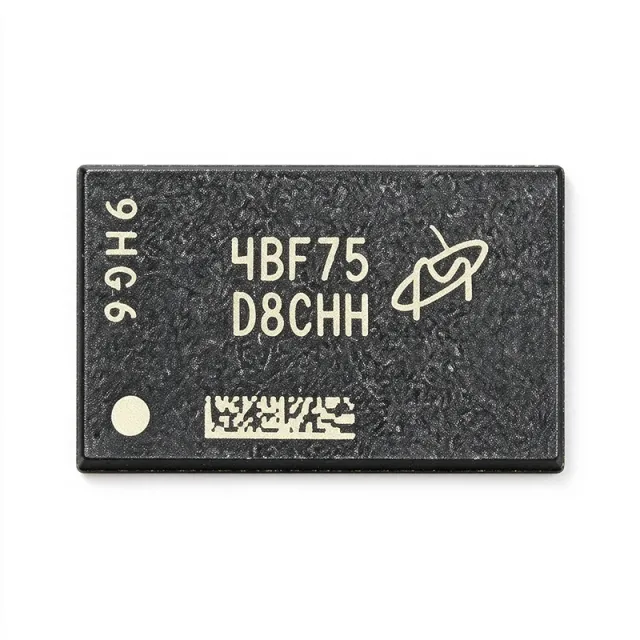
MT40A512M16TD-062E - 8Gb DDR4 SDRAM 512Mx16 1.2V | Micron
The Micron MT40A512M16TD-062E is an 8 Gbit DDR4 SDRAM memory IC organized as 512M x 16, operating at 3200 MT/s (1600 MHz clock, DDR4-3200) with a CAS latency of 22 (CL=19 ns access time), powered from a 1.2V core supply in a 96-ball FBGA package (7.5 x 13 mm). DDR4 SDRAM (Double Data Rate 4 Synchronous Dynamic Random-Access Memory) is a type of volatile memory that transfers data on both edges of the clock signal, effectively doubling the data rate relative to the internal clock. It is the successor to DDR3, offering higher speeds, lower operating voltage (1.2V vs 1.5V), and improved signal integrity. DDR4 is a critical component in modern computing systems, including servers, desktops, laptops, and embedded systems, where it serves as the main system memory. Key features of the MT40A512M16TD-062E include a 1.2V power supply, a 16-bit data bus, and support for data rates up to 3200 MT/s. It features programmable data strobe preambles, on-die termination (ODT), and a temperature-compensated self-refresh (TCSR) mode. The device also supports burst length of 8 (BL8) and burst chop of 4 (BC4), enabling flexible data access patterns. Technically, the MT40A512M16TD-062E utilizes Micron's advanced DRAM process technology, achieving high density and low power consumption. Its 16n prefetch architecture allows high-speed data transfer while maintaining internal core speeds. The device also features programmable read latency (RL) and write latency (WL), allowing system designers to optimize timing for their specific memory controller. Typical applications for this DDR4 SDRAM include server and data center memory modules, high-performance computing (HPC) systems, networking equipment, and advanced embedded systems. Its high density and speed make it ideal for applications requiring large memory capacity and fast data throughput, such as cloud computing, artificial intelligence, and real-time analytics. When designing with this device, ensure proper signal integrity by following Micron's layout guidelines, including controlled impedance traces and adequate decoupling capacitors. The device requires a stable 1.2V supply and a separate VPP supply of 2.5V for wordline boost. Careful attention to thermal management is also recommended. This page synthesizes distributor pricing, drop-in alternatives across Micron, Alliance Memory, Nanya, ISSI and Samsung, and practical design notes not found in the manufacturer datasheet.
MT40A512M16TD-062E AUT:R - 8Gbit DDR4 SDRAM | Micron
The Micron Technology MT40A512M16TD-062E AUT:R is an 8 Gbit DDR4 SDRAM memory IC organized as 512M x 16, operating at a 1.6 GHz data rate with 19 ns access time, supplied at 1.2 V and housed in a 96-ball FBGA (7.5 x 13 mm) package with AEC-Q100 automotive qualification. DDR4 SDRAM (Double Data Rate 4 Synchronous Dynamic Random Access Memory) is the fourth generation of the DDR DRAM family, a volatile memory technology that stores each bit in a capacitor-based cell refreshed on a regular cycle. In the memory hierarchy, it sits between CPU caches and storage, serving as the main working memory in automotive computing, industrial control, and networking systems. Key features of this device include the 8 Gbit monolithic die density, a x16 organization that simplifies 16-bit or 32-bit bus designs without byte-lane splitting, and the 1.2 V core supply that reduces power versus the 1.5 V DDR3 generation. The -062E speed grade supports DDR4-1600 class operation with 19 ns access latency. Architecturally, the part is a parallel-interface SDRAM with bank groups, on-die termination support, and an automotive temperature operating range denoted by the AUT grade in the part number. The -R suffix designates tape-and-reel packaging for automated surface-mount assembly. Typical applications include automotive infotainment and ADAS domain controllers, telematics gateways, and industrial HMI or edge-AI modules that require qualified DRAM with long-term supply. Design consideration: implement DDR4 controller training (write leveling, read training) and follow the Micron system design guidelines for fly-by routing and VTT termination on address/command lines. This page synthesizes distributor availability data, drop-in alternatives, and practical design notes not consolidated in the manufacturer datasheet.
MT40A512M8RH-075E:B - DDR4 4Gb 2666 MT/s SDRAM | Micron
The Micron Technology MT40A512M8RH-075E:B is a 4Gb DDR4 SDRAM memory IC organized as 512M x 8, operating at data rates up to 2666 MT/s (DDR4-2666 class, -075E speed grade) from a 1.2V VDD/VDDQ supply, housed in a 78-ball FBGA (TFBGA) package measuring 9 x 10.5 mm. DDR4 SDRAM (Double Data Rate 4 Synchronous Dynamic Random Access Memory) is the fourth generation of the JEDEC DDR memory family, sitting within the broader memory hierarchy of DRAM components used as main system memory in computing platforms. Compared to DDR3, DDR4 lowers the core supply voltage from 1.5V to 1.2V, doubles bank groups, and increases pre-fetch depth, delivering higher bandwidth at lower power per transfer. Key features of this device include VDD = VDDQ = 1.2V +/-60mV operation, an auxiliary VPP supply of 2.5V (-125mV/+250mV) for the DRAM cell word-line drivers, and on-die internally generated and adjustable VREFDQ, which simplifies board design by removing the need for an external reference voltage rail. The 1.2V pseudo open-drain I/O structure reduces power consumption on high-activity data buses. Architecturally, the part uses DDR4 bank-group interleaving to sustain high effective bandwidth, and supports refresh interval extensions at extended case temperature ranges. Internal VREFDQ generation improves signal-integrity margin and reduces BOM count. Typical applications include industrial PC main memory, embedded controllers, networking equipment, test and measurement systems, and automotive infotainment platforms (via the AIT automotive variant family). Design consideration: the DDR4-2666 speed grade requires careful length-matched routing and VTT termination on address/command lines; ball-map and layout guidance are provided in the Micron DDR4 datasheet and design guides. This page synthesizes distributor pricing context, drop-in alternatives, and practical design notes not found in the manufacturer datasheet.
MT40A512M8SA-062E - 4Gb DDR4 SDRAM x8, 3200 | Micron
The Micron Technology MT40A512M8SA-062E is a 4Gb DDR4 SDRAM memory IC organized as 512M x 8, operating at a clock frequency of 1.6 GHz (DDR4-3200 class) with VDD/VDDQ of 1.2V +/-60mV, packaged in a 78-ball FBGA (7.5 x 11 mm, Z10B) surface-mount package. DDR4 SDRAM (Double Data Rate 4 Synchronous Dynamic Random Access Memory) is the fourth generation of the DDR DRAM family, sitting within the hierarchy of DRAM components -> SDRAM -> DDR4 SDRAM -> volatile memory ICs. Compared to DDR3, DDR4 lowers the core supply voltage to 1.2V, doubles bank groups, and raises data rates up to 3200 MT/s, making it the dominant main-memory technology for computing platforms from embedded controllers to servers. Key features of this device include VDD = VDDQ = 1.2V +/-60mV with a separate VPP supply of 2.5V (-125mV/+250mV) for the word-line driver, on-die internal adjustable VREFDQ generation that eliminates an external reference rail, a pseudo open-drain 1.2V I/O interface, and TC maximum operation to 95 degrees C. The x8 organization supports the standard DDR4 feature set including bank groups and on-die termination. Technically, the device uses an 8n-prefetch architecture with two or four bank groups; data is transferred on both clock edges at up to 1600 MHz clock rate for 3200 MT/s effective bandwidth on the 8-bit data bus. The :F suffix denotes the lead-free/RoHS package flow with a commercial operating range; IT, AIT and AUT grade variants extend the range for industrial and automotive platforms. Typical applications include desktop and notebook main memory, embedded computing modules, industrial controllers, networking equipment, and replacement sourcing for DDR4-based designs. Design consideration: DDR4 routing requires length-matched, on-die-terminated data lines; PCB trace matching to the die, correct VPP decoupling, and address/command termination per the Micron datasheet layout guidance are essential for reliable operation at 3200 MT/s. This page synthesizes distributor pricing, drop-in alternatives across speed and temperature grades, and practical design notes not consolidated in the manufacturer datasheet.
MT41K128M16JT-125 AUT:K - 2Gbit DDR3L SDRAM 96-FBGA | Micron
The Micron Technology MT41K128M16JT-125 AUT:K is an automotive-grade DDR3L SDRAM memory IC delivering 2 Gbit of density organized as 128M x 16, operating at 800 MHz with a data rate of 1600 MT/s, housed in a 96-ball FBGA (8 x 14 mm) package. DDR3L SDRAM (Double Data Rate 3 Low Voltage synchronous dynamic random access memory) is a JEDEC-standard DRAM family that stores data in capacitor-based cells refreshed at regular intervals. Within the memory hierarchy, it sits between embedded SRAM and high-density storage, serving as the primary working memory for processors, SoCs, and FPGAs. The 'L' designation denotes low-voltage operation at 1.35V, fully backward compatible with 1.5V DDR3 systems per JEDEC specifications. Key features include 2 Gbit density in a single 128M x 16 organization, a -125 speed grade supporting 1600 MT/s data transfers, an automotive operating temperature range of -40C to +125C, and 1.35V nominal supply for reduced power consumption versus 1.5V DDR3. The AUT:K suffix identifies Micron's automotive product line with extended quality screening. Technically, the device uses an 8n-prefetch architecture internal to the core, with programmable CAS latency, on-die termination (ODT), and asynchronous reset support per DDR3L standards. The 16-bit wide data interface simplifies layout versus x32 parts and allows stacking multiple devices for 32-bit or 64-bit buses in embedded compute modules. Typical applications include automotive infotainment and telematics systems, ADAS sensor fusion platforms requiring validated memory, industrial control and human-machine interfaces, and network equipment operating over extended temperature ranges. Design consideration: DDR3L signal integrity demands length-matched fly-by routing of address/command lines, per-byte-tree data routing, and careful VTT termination; the 96-FBGA (8x14) footprint requires controlled-impedance PCB stackup for 1600 MT/s operation. This page synthesizes distributor pricing, drop-in alternatives, application guidance, and FAQ content not consolidated in the manufacturer datasheet.
MT41K128M16JT-125-ITK - 2Gb DDR3L SDRAM 1.35V | Micron
The Micron MT41K128M16JT-125-ITK is a 2 Gbit DDR3L SDRAM memory IC organized as 128M x 16, operating at 800 MHz clock frequency (DDR3L-1600 data rate) from a 1.35 V supply in a 96-ball FBGA (8x14 mm) package. DDR3L SDRAM is the low-voltage version of the DDR3 SDRAM standard, operating at 1.35 V instead of 1.5 V while remaining backward compatible: the device can also run in 1.5 V DDR3-compatible mode, in which case the 1.5 V DDR3 datasheet specifications apply. In the memory hierarchy it sits in the DRAM component category, serving as main-system memory downstream of processors, FPGAs, and SoCs that include an integrated DDR3/DDR3L memory controller. Key features of the -125 IT:K grade include an industrial operating temperature range of -40C to +95C, auto self-refresh, auto precharge, asynchronous reset, data mask (DM) for byte-wise write masking, dynamic on-chip termination (ODT), ZQ calibration, and write leveling - features that simplify controller bring-up and signal integrity at 1600 MT/s. Technically, the device uses an 8n-bit prefetch architecture with a bidirectional differential data strobe (DQS) and a fly-by command/address topology. The 16-bit organization requires only one chip per 16-bit memory bus, reducing BOM cost and layout complexity in space-constrained industrial designs. The 96-ball FBGA (8x14) lead-free package supports standard DDR3 routing with length-matched trace groups. Typical applications include FPGA-based industrial controllers (e.g., Xilinx 7-series with MIG controller), embedded Linux single-board computers, networking line cards, test and measurement instruments, and vision systems buffering image sensor data. Design consideration: DDR3L fly-by routing requires careful length matching within byte lanes; use the vendor MIG/IP core and follow Micron's DDR3 design guide for ODT and ZQ resistor placement (240 ohm, 1% to ZQ pin). This page synthesizes distributor pricing, drop-in cross-references, and practical DDR3L design notes not found in the manufacturer datasheet.
MT41K128M16JT-125:K - 2Gb DDR3L SDRAM 1600MT/s | Micron Technology
The Micron Technology MT41K128M16JT-125:K is a 2 Gbit DDR3L SDRAM memory IC organized as 128M words x 16 bits, operating at a 800 MHz clock (1600 MT/s data rate) with a 13.75 ns clock cycle time, housed in a 96-ball FBGA (8x14 mm) package. DDR3L SDRAM (Low-Voltage Double Data Rate 3 Synchronous Dynamic Random Access Memory) is a category of DRAM components that maintains a synchronous interface with a memory controller while transferring data on both edges of the clock. In the system memory hierarchy, it sits between the memory controller and the storage layer, serving as the primary volatile working memory of an embedded or computing platform. DDR3L reduces core supply from 1.5V to 1.35V, cutting dynamic power roughly 20% versus DDR3 while remaining backward compatible on most controllers. Key features of this part include the 8n-bit prefetch architecture, auto self-refresh, write leveling, data mask (DM) support, dynamic on-die termination (ODT), and an asynchronous reset function. The -125 speed grade supports DDR3L-1600 operation with CL=11 timing. The commercial temperature rating of 0C to +95C covers the standard JEDEC DRAM operating envelope for desktop, networking, and consumer platforms. Technically, the device uses an 8n-bit prefetch internal architecture with bank groups of eight internal banks, 1.35V (1.283V-1.45V) supply, and on-die termination with dynamic ODT targeting to simplify signal integrity at 1600 MT/s. The 96-FBGA ball map provides a short, controlled flight time for address/command and data lines, enabling fly-by routing of the address/command bus as required by DDR3 controllers. Typical applications include embedded processor and FPGA memory subsystems, industrial HMI and networking line cards, set-top boxes, and x16 data paths in general computing platforms where a single 2 Gbit device provides the full 16-bit bus width. A key design consideration is VTT termination: the fly-by C/A topology requires properly designed VTT rails and series damping resistors, and controller write leveling must be enabled to close timing across the ball map. This page synthesizes distributor pricing, drop-in same-package alternatives, and practical DDR3L design notes not found in the manufacturer datasheet.
MT41K256M16 - 4Gb DDR3L SDRAM 1.35V x16 | Micron Technology
The Micron Technology MT41K256M16 is a 4Gb (256M x 16) DDR3L SDRAM memory IC operating from a 1.35V supply, housed in a 96-ball FBGA package. It is the low-voltage version of DDR3 (1.5V) SDRAM and remains pin- and protocol-compatible when run in 1.5V DDR3 mode, per the Micron 4Gb x4/x8/x16 DDR3L datasheet. DDR3L SDRAM is a class of synchronous dynamic random-access memory that transfers data on both clock edges (double data rate) and uses a source-synchronous strobe-based interface. Within the memory hierarchy, the MT41K256M16 sits at the component level of DRAM main memory, below DIMM modules and above the raw DRAM core, serving as the primary working memory for processors, FPGAs, and SoCs. Key features of the MT41K256M16 family include the 4Gbit single-die density organized as 256 megawords x 16 bits, an internal 8-bank architecture for improved parallelism, and a 1.35V VDD supply with 1.5V-compatible operation. The x16 organization reduces external component count in 16-bit or 32-bit bus systems compared with x4/x8 parts, which use a different 78-ball outline. Speed grades in the family span DDR3L-1066 through DDR3L-2133 (for example -125 and -093/-107 suffices), with the exact speed grade encoded in the full ordering MPN such as MT41K256M16TW-107:P or MT41K256M16RE-125. On-die termination (ODT), DLL-based timing, and programmable CAS latency provide signal-integrity and latency tuning options for FPGA and processor memory controllers. Typical applications include embedded processor memory for Xilinx Zynq and Artix/Kintex FPGA platforms, industrial controllers, networking equipment, automotive infotainment, and consumer electronics where a 512 MB single-chip address space at 1.35V is required. Design considerations: DDR3L Fly-by routing, VTT termination, and ZQ calibration resistor placement dominate layout quality. Always derate address/command timing at elevated temperature, and confirm the JEDEC-required initialization sequence in the memory controller. This page synthesizes distributor sourcing data, cross-brand drop-in equivalents (Samsung, Nanya), and practical DDR3L design notes not found in the standard Micron datasheet, with pricing as of 2026-10-11.
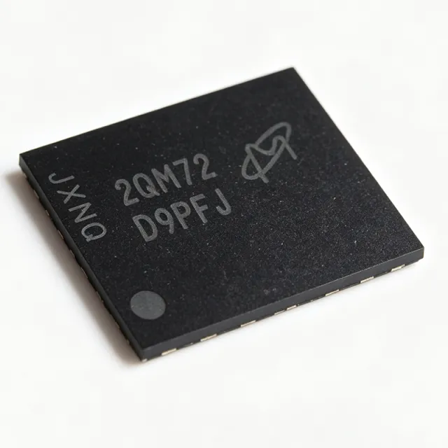
MT41K256M8DA-125 - 2Gb DDR3L SDRAM x8 800MHz | Micron
The Micron Technology MT41K256M8DA-125 is a 2Gbit DDR3L SDRAM memory IC organized as 256M x 8, operating at a data rate of 800 MT/s (400 MHz clock, CL=11 at 13.75 ns) from a 1.35V supply, housed in a 78-ball FBGA (8 mm x 10.5 mm) package. DDR3L SDRAM is a low-voltage version of the JEDEC-standard DDR3 SDRAM. DDR3 doubles the data rate of DDR2 by using an 8-bit prefetch architecture and fly-by-terminated signal routing, while DDR3L further reduces core power by operating at 1.35V instead of 1.5V. It is also backward compatible with 1.5V DDR3 operation per Micron documentation. DRAM components like this device form the main-memory tier of the memory hierarchy, sitting between CPU caches and storage, and are managed by a DDR memory controller on the host processor or chipset. Key features include 8 internal banks, programmable CAS latency, two fixed burst lengths (BL8 and BC4 via mode register or on-the-fly), auto self-refresh and auto precharge, an asynchronous reset pin for fast initialization, data mask (TDQS/DM) support, dynamic on-die termination (ODT), ZQ output driver calibration, and write leveling for fly-by topology signal integrity. Technically, the device uses an 8n-bit prefetch architecture with a SSTL-15 compatible I/O interface (1.35V nominal) and supports derated timing at elevated temperature. The -125 speed grade corresponds to 13.75 ns CL=11 timing at 800 MT/s. The industrial-grade IT variant extends operation to -40C to +95C. Typical applications include embedded systems main memory, industrial PCs, networking equipment, set-top boxes, and test instrumentation requiring compact, low-power DRAM in a space-saving FBGA footprint. Design consideration: DDR3L fly-by routing requires per-device write leveling in the memory controller; verify ODT settings and ZQ calibration resistor placement per the Micron datasheet layout guidelines. This page synthesizes distributor pricing, drop-in alternatives, and practical design notes not found in the manufacturer datasheet.
MT41K512M16HA-125:A - 8Gb DDR3L SDRAM 1.35V | Micron Technology
The Micron Technology MT41K512M16HA-125:A is an 8 Gbit DDR3L SDRAM memory IC organized as 512M x 16, operating at 800 MHz clock (DDR3-1600 data rate, 13.75 ns access time) from a 1.35 V supply in a 96-ball FBGA (9 x 14 mm) package. DDR3L SDRAM is the low-voltage version of DDR3 (1.5 V) SDRAM and is a cornerstone of modern volatile memory hierarchies. Within the memory hierarchy, SDRAM sits below CPU caches as main-system or working memory: a DRAM core organized into banks stores each bit as charge in a capacitor cell, refreshed periodically, and a synchronous interface (clocked by CK/CK#) pipelines commands to achieve high bandwidth. DDR3L parts like this one can also run in DDR3 (1.5 V) compatible mode per the manufacturer datasheet. Key features include 8 internal banks, an 8n-bit prefetch architecture, differential bidirectional data strobes (DQS/DQS#), differential clock inputs (CK/CK#), and programmable nominal and dynamic on-die termination (ODT) for data, strobe, and mask signals. The x16 organization simplifies 16-bit and 32-bit memory bus designs for embedded processors. The commercial operating range is 0C to +95C (Mouser lists the extended variant to 95C; the Alliance listing specifies 0C to 90C). Architecturally, the 8-bank array with 8n prefetch and double-data-rate strobing delivers DDR-1600 bandwidth per pin while the ODT and programmable CAS latency settings let controllers tune signal integrity on fly-by or tee-topology DDR3 buses. The 96-ball FBGA (PBGA-96) surface-mount package minimizes loop inductance for clean high-speed signaling. Typical applications include embedded main memory for industrial and networking processors, set-top boxes, automotive infotainment head units (using AIT grade variants), and memory expansion modules on single-board computers. Design consideration: DDR3L requires proper VTT/VDDQ termination and length-matched routing per JEDEC-style DDR3 layout practice; always verify controller compatibility (ODT settings, CAS latency) before board spin. This page synthesizes distributor pricing, drop-in alternatives from Micron, Alliance Memory, and ISSI, and practical DDR3L design notes not found in the manufacturer datasheet. Pricing as of 2026-09-10.
MT41K512M16VRP-107 - 8Gb DDR3L SDRAM 933MHz | Micron
The Micron Technology MT41K512M16VRP-107 IT:P is an 8Gbit automotive DDR3L SDRAM organized as 512M x 16, operating at 933 MHz (DDR3-1866) with 20 ns access time, housed in a 96-ball FBGA (8 x 14 mm) package. It is a TwinDie device that combines two Micron 4Gb DDR3L x8 die in a single package to form a 2-byte wide x16 memory. DDR3L SDRAM (Low-Voltage Double Data Rate 3 Synchronous DRAM) is a type of volatile dynamic random-access memory that operates at 1.35V nominal, while remaining backward-compatible with 1.5V DDR3 operation. Within the memory hierarchy, SDRAM components sit at the DRAM level, providing the main system memory for processors, and DDR3L occupies the mid-generation position between DDR2 and DDR4. This TwinDie construction doubles density without requiring larger packages or finer process nodes at the module level. Key features of the MT41K512M16VRP-107 include the wide industrial-plus operating temperature range of -40C to +95C (the IT suffix), automotive-grade screening (the :P designation), 1.35V low-voltage core operation for reduced power, and an asynchronous reset function for reliable initialization. Additional capabilities include auto self-refresh, auto precharge, data mask, dynamic on-die termination (ODT), and write leveling, which simplifies high-speed signal-integrity tuning on DDR3 controller interfaces. The TwinDie architecture uses two 4Gb DDR3L x8 die internally; according to Micron, specifications for the base part MT41K512M8 correlate to the TwinDie manufacturing base part MT41K512M16, and the manufacturer datasheet should be read together with the 4Gb x8 data sheet for parameters not covered in the 16-page TwinDie document. Typical applications include automotive infotainment and telematics main memory, ADAS sensor fusion platforms, industrial gateways and embedded controllers, and rugged networking equipment that requires high-density DRAM across extended temperatures. The automotive qualification makes this part particularly suited to designs where AEC-grade component selection is a system requirement. A key design consideration: the TwinDie device presents two chip-select domains internally, so controller configuration and address mapping must match the datasheet dual-die organization, and 96-ball FBGA solder profiles must follow automotive reflow requirements. This page synthesizes distributor pricing, drop-in alternatives, and practical design notes not found in the manufacturer datasheet, with pricing as of 2026-09-10.
MT41K512M8DA-107 IT:P - 4Gb DDR3L SDRAM x8 | Micron
The Micron MT41K512M8DA-107 IT:P is a 4Gb DDR3 SDRAM organized as 512M x 8, packaged in a 78-ball TFBGA, with the IT suffix denoting industrial temperature operation from -40C to +95C and the P suffix denoting lead-free, RoHS-compliant construction. It operates at DDR3-1866 data rates per Micron's -107 speed grade designation. A DDR3 SDRAM (Double Data Rate Type Three Synchronous Dynamic Random Access Memory) is a type of volatile memory IC that transfers data on both clock edges, doubling bandwidth relative to single data rate DRAM at the same clock frequency. Within the memory hierarchy it sits as main-system memory, alongside DRAM controllers, memory ICs, and semiconductor components in the broader integrated circuit taxonomy. DDR3 operates at 1.5V and uses an 8n prefetch architecture, on-die termination (ODT), write leveling, and auto self-refresh to sustain high data rates while managing signal integrity. Key features of this part per distributor data include 4Gbit density in a x8 organization, Auto self-refresh, Auto precharge, an asynchronous reset function, data mask capability, dynamic on-die termination, and write leveling. The industrial temperature range (-40C to +95C) makes it suitable for environments beyond standard commercial 0C to +85C operation, and the TFBGA ball-grid package provides short, low-inductance interconnects for high-speed signal routing. Architecturally, the 512M x 8 organization maps to internal banks accessed through a standard DDR3 command interface with RAS, CAS, WE, chip select, bank address, and row/column address pins. The -107 grade supports DDR3-1866 timing, requiring a memory controller configured for the corresponding JEDEC speed bin. Designers must confirm exact CAS latency, tRCD, tRP, and supply class (1.5V vs 1.35V DDR3L) from the official Micron datasheet before finalizing a design. Typical applications include industrial control and automation systems, networking and communication equipment, test and measurement instrumentation, and embedded computing platforms that require high-density DRAM with industrial-grade temperature tolerance. A key design consideration: DDR3 signal integrity at 1866 Mbps requires careful fly-by termination routing, matched trace lengths, and ODT calibration; the 78-ball TFBGA footprint also demands precise PCB land pattern adherence per the Micron package drawing. This page synthesizes distributor inventory data, the verified industrial-temperature and RoHS suffix coding, and family cross-reference information not consolidated in the manufacturer datasheet.
MT41K64M16TW-107 - 1Gbit DDR3L SDRAM 1866MT/s | Micron Technology
The Micron Technology MT41K64M16TW-107 is a 1Gbit DDR3L SDRAM memory IC organized as 64M x 16, operating at up to 933 MHz (DDR3-1866 data rate of 1866 MT/s, 20 ns cycle time) from a 1.35 V supply, housed in a 96-ball FBGA (8 x 14 mm) package. DDR3L SDRAM (Double Data Rate 3 Low Voltage) is a class of synchronous dynamic random-access memory that transfers data on both clock edges and operates from a reduced 1.35 V core supply instead of the 1.5 V used by standard DDR3. As a DRAM component in the memory hierarchy, it sits between embedded SRAM caches and mass storage, providing the main working memory for processors and FPGA-based systems. DDR3L devices are backward-compatible with 1.5 V DDR3 systems when run in 1.5 V compatible mode. Key features of this device include its 1 Gbit density in a x16 I/O width, an industry-standard 1866 speed grade (-107), and low-voltage operation at 1.35 V (nominal range 1.283 V to 1.45 V), which reduces memory subsystem power relative to 1.5 V DDR3. The 96-ball FBGA (PBGA-96) surface-mount package offers excellent signal integrity for high-speed address, command, and data buses. Technically, the device uses CMOS DRAM core technology with double-data-rate I/O, 8n-bit prefetch architecture, and supports standard DDR3 functions such as on-die termination (ODT) and the RESET# pin for defined power-up state. According to Micron product data, the part operates over a 0C to +95C case temperature range in the standard (non-IT) grade, with industrial (-IT, -40C to +95C) and automotive (-AIT) grade variants sharing the same silicon and footprint. Typical applications include embedded processor memory, FPGA companion memory (Microchip, Xilinx/AMD boards), industrial controllers, networking equipment, and set-top/consumer platforms where a single 1 Gbit x16 DDR3L device supplies the entire system memory. A key design consideration: DDR3L fly-by routing requires careful length matching of the clock, command, and address lines, and VTT termination must be provided on the controller side; verify the controller supports DDR3L levels or enable 1.5 V compatible mode. This page synthesizes distributor pricing, drop-in alternatives across temperature grades and brands, and practical DDR3L design notes not found in the manufacturer datasheet.
MT41K64M16TW-107 AAT:J - 1Gbit DDR3L SDRAM 933MHz | Micron
The Micron Technology MT41K64M16TW-107 AAT:J is a 1Gbit DDR3L SDRAM memory IC organized as 64M x 16, operating at 933 MHz clock frequency (DDR3L-1866) with a 20 ns access time and 1.35 V supply, housed in a 96-ball FBGA (8x14 mm) package. It is an automotive-grade, AEC-Q100 qualified DRAM targeted at demanding embedded platforms. DDR3L SDRAM (Double Data Rate 3 Low Voltage) is a synchronous dynamic random-access memory that transfers data on both clock edges, doubling effective bandwidth relative to SDR DRAM. Within the memory hierarchy, DRAM sits between CPU caches and storage, serving as main system memory or frame-buffer memory in processors, SoCs, FPGAs, and multimedia platforms. Key features include the wide 64M x 16 organization that simplifies 16-bit memory buses, the 1.35 V low-voltage core that cuts dynamic power versus 1.5 V DDR3, a 933 MHz clock rate delivering up to 1866 MT/s of data rate, and the compact 96-FBGA (8x14) ball-grid package suited to dense multilayer PCBs. The 'A' grade prefix and 'AAT' temperature suffix denote automotive qualification for extended environmental stress. Architecturally, the device uses an 8-internal-bank DDR3L core with standard burst-length-8 operation, on-die termination (ODT), and JEDEC-standard DDR3L command interface, allowing use with mainstream memory controllers from Texas Instruments, NXP, Xilinx/AMD, and STMicroelectronics. Typical applications include automotive infotainment and instrument clusters, industrial programmable-logic and vision systems, and networking line-card buffer memory where AEC-Q100 qualification is mandatory. Design consideration: DDR3L signal integrity requires length-matched, impedance-controlled routing (40-60 ohm traces), VTT termination, and careful fly-by address routing per Micron's DDR3 system design guidance. This page synthesizes distributor pricing, drop-in same-footprint alternatives, and practical DDR3L layout notes not found on the manufacturer product page.