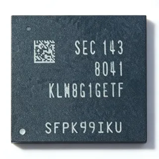
K4A8G085WC - 8Gb DDR4 SDRAM 1Gx8 2666Mbps | Samsung Electronics
MPN: K4A8G085WC ✓ Active| Qty | Unit Price | Extended |
|---|---|---|
| 1 | $29.36 | $29.36 |
| 10 | $28.5 | $285.00 |
| 100 | $27.2 | $2,720.00 |
| 500 | $26.1 | $13,050.00 |
| 1,000 | $24.9 | $24,900.00 |
K4A8G085WC Overview
DDR4 SDRAM (Double Data Rate 4 Synchronous Dynamic Random Access Memory) is the fourth generation of DDR memory, the dominant class of volatile main memory in computing systems. In the memory hierarchy, this component sits at the DRAM device level below memory modules (DIMMs) and above NAND flash for working-storage duty, serving as main memory for processors, FPGAs, and SoCs.
Key features include the 8 Gbit density in a single x8 organization, 2666 Mbps/pin bandwidth, and a low 1.2 V core supply (operating window 1.14 V to 1.26 V) that reduces power versus DDR3. The device provides auto precharge, asynchronous reset, CRC and parity support, ZQ calibration, dynamic on-chip termination (ODT), and data mask (DM) functions - all critical for signal integrity and data reliability at DDR4 speeds.
Architecturally, the die uses Samsung's advanced DRAM process with bank-group architecture enabling high internal parallelism, and DBI (data bus inversion) plus CRC features lower I/O power and improve bit error performance on high-speed links. The 78FBGA ball map follows the standard x8 DDR4 component footprint, enabling multi-sourcing on the same PCB land pattern.
Typical applications include industrial controllers and embedded systems (especially the -BITD industrial temperature variant), networking and communication equipment, FPGA-based processing boards, and test and measurement systems requiring gigabyte-class main memory with proven DDR4 controller IP.
Design consideration: DDR4 trace-length matching, ZQ resistor placement (240 ohm 1%), and VTT termination rail design dominate layout effort; verify controller speed-bin support (2666) and temperature class against your ordering suffix before finalizing the BOM.
This page synthesizes distributor stock and pricing, drop-in alternatives from Micron, SK Hynix, and Nanya, and practical design notes not found in the Samsung datasheet, with pricing as of 2026-09-06.
Drop-in alternatives for K4A8G085WC — same package, pin-to-pin compatible. Different-package parts requiring PCB rework are excluded.
Variants in this series
Same-series models that are drop-in compatible with K4A8G085WC (same form factor and footprint) — differing in Package, Burst Length, Data Rate, Density, Organization.
Quick Comparison Tool — Select alternative parts for side-by-side comparison:
K4A8G085WC-BITD
✅ Drop-In📋 Reference alternative (not in catalog)
K4A8G085WC-BCTD
✅ Drop-In✓ In Stock
$50.85 / Unit
View Datasheet →K4A8G085WC-BIWE
✅ Drop-In✓ In Stock
$6.29 / Unit
View Datasheet →K4A8G085WB-BCPB
✅ Drop-In✓ In Stock
$3.28 / Unit
View Datasheet →MT40A1G8SA-075E
✅ Drop-In📋 Reference alternative (not in catalog)
H5AN8G6NAFR-UHC
✅ Drop-In✓ In Stock
$0.12 / Unit
View Datasheet →NT6AN8T1GA4H1-H1
✅ Drop-In📋 Reference alternative (not in catalog)
K4A8G085WC Maximum Ratings & Electrical Characteristics
| Memory Type | DDR4 SDRAM |
| Density | 8 Gbit |
| Organization | 1G x 8 |
| Speed | 2666 Mbps/pin (DDR4-2666) |
| Supply Voltage | 1.2 V |
| Supply Voltage Range | 1.14 V to 1.26 V |
| Clock Frequency | 1333 MHz (1333.333 GHz nominal, per web data) |
| Operating Temperature (K4A8G085WC-BITD) | -40 C to +95 C |
| Operating Temperature (K4A8G085WC-BCTD) | 0 C to +95 C |
| Package | 78-ball FBGA (78FBGA) |
| Mounting Type | Surface Mount |
| Auto Precharge | Yes |
| Asynchronous Reset | Yes |
| CRC Function | Yes |
| ZQ Calibration | Yes |
| Dynamic On-Chip Termination (ODT) | Yes |
| Data Mask (DM) | Yes |
K4A8G085WC 78-ball fbga (78fbga) Pin Configuration Guide
Pin configuration for K4A8G085WC (78-ball fbga (78fbga) package). This digital IC includes GPIO, communication interfaces (UART, SPI, I2C), and power pins. Refer to the manufacturer datasheet for alternate pin functions and configuration options. Essential for embedded system design and PCB layout.

No detailed pinout data available for K4A8G085WC.
Refer to the datasheet for full pin configuration.
Typical Applications
K4A8G085WC is suitable for 6 applications: Industrial Controllers and Automation, Networking and Communication Equipment, FPGA-Based Processing and Prototyping Boards, Embedded Computing and Industrial PCs, Test and Measurement Instrumentation, Automotive and Telematics Adjacent Systems.
Industrial Controllers and Automation
The K4A8G085WC-BITD variant, rated -40 C to +95 C, is purpose-suited to PLCs, industrial gateways, and machine-vision controllers that must survive unconditioned cabinets and thermal cycling. Its 8 Gbit (1 GB) density provides working memory for protocol stacks, edge analytics, and logging buffers, while the x8 organization lets designers scale width with multiple devices. DDR4's 1.2 V supply lowers system power versus DDR3, easing convection-cooled designs. Placed on a length-matched fly-by address bus with on-chip termination enabled, the device sustains DDR4-2666 (2666 Mbps/pin) with CRC and ZQ calibration supporting data integrity in electrically noisy factory environments. Verify industrial temperature grade on the ordering suffix at BOM time.
Recommended
Networking and Communication Equipment
Switches, routers, and 5G small-cell equipment rely on gigabyte-class DDR4 for packet buffers, routing tables, and control-plane software. The K4A8G085WC's 2666 Mbps/pin data rate and x8 organization deliver about 2.67 GB/s per device, and CRC plus data-bus features protect long-flight-time links typical of multi-chip networking boards. The 78FBGA footprint supports 4-8 device topologies on the same land pattern for width scaling to 32- or 64-bit buses. Dynamic ODT reduces termination power in heavily loaded buses, and the asynchronous reset function simplifies hot-reset handling in carrier-grade chassis where managed reset sequencing is mandatory.
Recommended
FPGA-Based Processing and Prototyping Boards
Intel/Altera and Xilinx FPGA boards commonly use x8 DDR4 components such as the K4A8G085WC because 64-bit buses are built from eight identical devices sharing one fly-by command/address tree. The 1G x 8 organization matches vendor memory-controller IP (Intel EMIF, Xilinx MIG) training routines, and ZQ calibration plus write-leveling are handled automatically during initialization. At DDR4-2666 the device provides roughly 21.3 GB/s aggregate bandwidth with eight devices, sufficient for video frame buffering, DSP datapaths, and HPC prototyping. The multi-source 78FBGA ballout (Samsung/Micron/SK Hynix equivalents) de-risks FPGA board BOMs against DDR4 EOL churn.
Recommended
Embedded Computing and Industrial PCs
Embedded x86 and ARM motherboards use 1G x 8 DDR4 components like the K4A8G085WC in soldered-down (memory-down) configurations for vibration-resistant, small-footprint industrial PCs and box PCs. Memory-down avoids SO-DIMM connector reliability issues in mobile and vehicle-mounted systems while saving board area and cost. The 1.2 V rail simplifies power sequencing with common DDR4 PMICs, and the -BITD industrial grade covers -40 C to +95 C ambient extremes. Designers should implement per Intel or CPU-vendor DDR4 layout guidelines, use VTT termination with proper decoupling, and validate at DDR4-2666 with margin testing across the temperature range.
Recommended
Test and Measurement Instrumentation
Oscilloscopes, logic analyzers, and signal generators require deep capture memory and fast instrument-state storage, making 8 Gbit DDR4 devices a cost-effective capture buffer. The K4A8G085WC's 2666 Mbps/pin rate sustains streaming acquisition data into a ring buffer, while 1 GB per device allows stacking multiple devices for gigabytes of capture depth. The x8 organization's DM (data mask) function simplifies partial writes used in segmented-capture schemes. Bench instruments operate at commercial temperatures, so the -BCTD grade (0 C to +95 C) suffices, offering lower-cost sourcing than the industrial -BITD. CRC and ODT maintain signal integrity across long backplane-style routing.
Recommended
Automotive and Telematics Adjacent Systems
While standard DDR4 is not AEC-Q100 qualified, the K4A8G085WC-BITD's -40 C to +95 C rating makes it usable in non-safety telematics, fleet-tracking gateways, and dashboard-adjacent infotainment dongles where cost matters and AEC-Q100 is not contractually required. Its 1.2 V operation reduces thermal load in sealed enclosures, and the 8 Gbit density supports map caching and OTA update staging. Designers must add their own qualification coverage (thermal cycling, HTOL) for automotive programs. The 78FBGA soldered-down format withstands vibration better than socketed modules, and asynchronous reset supports ignition-switched power topologies with controlled power-down sequencing.
Recommended
Recommended Products Summary
Engineering reference data for K4A8G085WC — comparison, design guidance, and compliance information.
Selection Guide
Comparison with Alternatives
| Parameter | This Product | K4A8G085WC-BITD | K4A8G085WC-BIWE | MT40A1G8SA-075E | H5AN8G6NAFR-UHC | NT6AN8T1GA4H1-H1 |
|---|---|---|---|---|---|---|
| Brand | Samsung Electronics | Samsung Electronics | Samsung Electronics | Micron Technology | SK Hynix | Nanya Technology |
| Package | 78FBGA | 78FBGA - same | 78FBGA - same | 78FBGA - same | 78FBGA (FBGA-78) - same | 78FBGA - same |
| Density / Organization | 8 Gbit / 1G x 8 | 8 Gbit / 1G x 8 | 8 Gbit / 1G x 8 | 8 Gbit / 1G x 8 | 8 Gbit / 1G x 8 | 8 Gbit / 1G x 8 |
| Supply Voltage | 1.2 V (1.14-1.26 V) | 1.2 V | 1.2 V | 1.2 V | 1.2 V | 1.2 V |
| Features | Auto precharge, async reset, CRC, ZQ cal, dynamic ODT, DM | Same feature set (same die) | Same family feature set | Standard DDR4 feature set (CRC, ODT, ZQ) | Standard DDR4 feature set | Standard DDR4 feature set |
Key Differentiators
- Industrial temperature grade available in same footprint (vs MT40A1G8SA-075E)
- Cross-brand second sourcing on identical land pattern (vs K4A8G085WC-BIWE)
- Low 1.2 V operation with power-saving features (vs K4A8G085WB-BCPB)
Design Notes
DDR4 x8 layout with the K4A8G085WC demands discipline: route address/command in fly-by topology with per-device stubs under 5 mm, keep DQ/DQS/DM byte groups length-matched within about +/-25 mils (0.6 mm) intra-byte, and maintain continuous reference planes. Place the 240 ohm 1% ZQ resistor within a few millimeters of the ZQ ball with a dedicated ground via; do not share this trace. Follow Samsung's DDR4 design guide and your controller vendor (Intel EMIF / Xilinx MIG) checklist before tape-out.
Provide a regulated 1.2 V core rail (1.14-1.26 V window) plus a separate VTT termination rail sourced from a DDR4 VTT regulator with at least 0.5 x VDDQ termination current capability, decoupled with bulk and high-frequency ceramic banks at every other ball row. Estimated: eight devices on a 64-bit bus at DDR4-2666 can draw on the order of 1-2 W total system memory power depending on utilization - budget VTT droop and add bulk capacitance near the regulator. Sequence VDDQ before or with VPP/VTTER per JEDEC-style DDR4 reset behavior; use the asynchronous reset ball for controlled re-initialization.
The most frequent DDR4 substitution failures come from ignoring ordering-code details: die revision (WB vs WC), speed bin, and temperature suffix (-BITD vs -BCTD) all change timing tables and thermal limits. Cross-brand swaps (Micron MT40A1G8SA-075E, SK Hynix H5AN8G6NAFR-UHC) share the 78FBGA footprint but require re-running controller memory training/write-leveling and re-verifying read/write margins at temperature extremes. Also confirm Samsung PCN/EOL status - 2026 migration guides indicate legacy DDR4 die are being sunset toward DDR5/HBM production.
Compliance Information
Compliance declarations not present in provided web data; Samsung DRAM components are typically RoHS compliant but this must be confirmed via Samsung's official eco-compliance documentation.