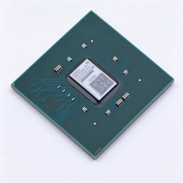
XC7K70T-1FBG676C - Kintex-7 FPGA 65,600 Cells | AMD
MPN: XC7K70T-1FBG676C ✓ Active| Qty | Unit Price | Extended |
|---|---|---|
| 1 | $62.7273 | $62.73 |
| 10 | $45.303 | $453.03 |
| 100 | $40.0758 | $4,007.58 |
| 500 | $38.3333 | $19,166.65 |
| 1,000 | $36.5909 | $36,590.90 |
XC7K70T-1FBG676C Overview
A Field Programmable Gate Array (FPGA) is an integrated circuit that can be configured by the customer after manufacturing to implement any digital logic function. FPGAs sit within the programmable logic device (PLD) hierarchy, above CPLDs, and are used for parallel processing, high-speed interfacing, and rapid prototyping. The Kintex-7 family balances cost, performance, and power for mid-range applications.
Key features include 300 user I/Os supporting various I/O standards, 4,976,640 bits of block RAM for data buffering, and 65,600 logic cells for implementing complex digital designs. The 28nm process enables high performance with reasonable power consumption. The lidless FCBGA package provides excellent thermal performance for high-density designs.
Technically, the XC7K70T-1FBG676C includes MMCM (Mixed-Mode Clock Manager) and PLL (Phase-Locked Loop) blocks for clock generation and management, supporting a wide range of clock frequencies. The device supports configuration via JTAG, SPI, and BPI interfaces, allowing flexible programming options. The 1V core voltage reduces dynamic power compared to older families.
Typical applications include software-defined radio, medical imaging, industrial automation, and aerospace/defense systems where high-speed signal processing and reconfigurability are required. The 300 I/Os enable interfacing with high-speed ADCs, DACs, and memory devices.
When designing with this FPGA, ensure adequate decoupling capacitors on all power pins and follow AMD's power-on sequencing guidelines. The lidless package requires careful thermal management; use a heatsink or forced airflow for high utilization designs.
Drop-in alternatives for XC7K70T-1FBG676C — same package, pin-to-pin compatible. Different-package parts requiring PCB rework are excluded.
Variants in this series
Same-series models that are drop-in compatible with XC7K70T-1FBG676C (same form factor and footprint) — differing in Block RAM, RoHS Status, Speed Grade.
Quick Comparison Tool — Select alternative parts for side-by-side comparison:
XC7K70T-2FBG676I
✓ In Stock
$19 / Unit
View Datasheet →XC7K325T-1FBG676C
✓ In Stock
$108 / Unit
View Datasheet →XC7K70T-2FBG676C
📋 Reference alternative (not in catalog)
XC7K70T-1FBG676I
📋 Reference alternative (not in catalog)
XC7K160T-1FBG676C
📋 Reference alternative (not in catalog)
XC7K70T-1FBG676C Maximum Ratings & Electrical Characteristics
| Family | Kintex-7 |
| Logic Cells | 65,600 |
| Block RAM | 4,976,640 bits |
| User I/Os | 300 |
| Process Technology | 28nm |
| Core Voltage | 1V |
| Package | 676-BBGA, FCBGA (lidless) |
| Number of Pins | 676 |
| Mounting Type | Surface Mount |
| Clock Management | MMCM, PLL |
| Configuration Interfaces | JTAG, SPI, BPI |
| Speed Grade | -1 |
| RoHS Status | Compliant (Pb-free) |
XC7K70T-1FBG676C Pin Configuration
| Pin A1 | IO_L1P_T0 — User I/O bank 0, differential pair P |
| Pin A2 | IO_L1N_T0 — User I/O bank 0, differential pair N |
| Pin B1 | VCCINT — Internal core voltage 1V |
| Pin B2 | GND — Ground |
| Pin C1 | IO_L2P_T0 — User I/O bank 0, differential pair P |
| Pin C2 | IO_L2N_T0 — User I/O bank 0, differential pair N |
| Pin D1 | VCCAUX — Auxiliary voltage 1.8V |
| Pin D2 | GND — Ground |
| Pin E1 | IO_L3P_T0 — User I/O bank 0, differential pair P |
| Pin E2 | IO_L3N_T0 — User I/O bank 0, differential pair N |
| Pin F1 | VCCINT — Internal core voltage 1V |
| Pin F2 | GND — Ground |
Typical Applications
XC7K70T-1FBG676C is suitable for 6 applications: Software-Defined Radio, Medical Imaging, Industrial Automation, Aerospace and Defense, High-Performance Computing, Test and Measurement.
Software-Defined Radio
The XC7K70T-1FBG676C is ideal for software-defined radio (SDR) systems due to its 300 user I/Os and 65,600 logic cells, enabling high-speed digital signal processing. It can interface with high-speed ADCs and DACs, supporting wideband signal processing. The MMCM and PLL blocks provide flexible clock generation for various frequency bands. Its 28nm process ensures low power consumption, critical for portable SDR units. The lidless FCBGA package allows efficient heat dissipation in compact enclosures.
Recommended
Medical Imaging
In medical imaging systems like ultrasound and CT scanners, the XC7K70T-1FBG676C provides the logic capacity for real-time image processing. Its 4,976,640 bits of block RAM enable efficient data buffering for image frames. The 300 I/Os connect to image sensors and display interfaces. The device's reliability and long-term availability make it suitable for medical equipment. The commercial temperature grade covers typical operating environments in hospitals.
Recommended
Industrial Automation
The XC7K70T-1FBG676C excels in industrial automation for motor control and machine vision. Its 65,600 logic cells can implement multiple control loops and vision algorithms. The 300 I/Os interface with encoders, sensors, and actuators. The 28nm process provides a balance of performance and power for 24/7 operation. The lidless FCBGA package supports reliable operation in industrial environments with proper cooling.
Recommended
Aerospace and Defense
For aerospace and defense applications, the XC7K70T-1FBG676C offers the reconfigurability needed for radar and communication systems. Its 65,600 logic cells can implement complex signal processing chains. The device supports secure configuration via JTAG and SPI. The commercial temperature grade is suitable for ground-based systems, while the industrial variant is available for harsher environments. AMD's long-term supply commitment supports defense program lifecycles.
Recommended
High-Performance Computing
In high-performance computing (HPC) accelerators, the XC7K70T-1FBG676C provides parallel processing capabilities for data-intensive tasks. Its 65,600 logic cells can implement custom arithmetic units and data paths. The 300 I/Os enable high-bandwidth connections to host processors and memory. The 28nm process offers competitive performance-per-watt. The lidless FCBGA package allows efficient thermal management in server environments.
Recommended
Test and Measurement
The XC7K70T-1FBG676C is well-suited for test and measurement equipment like oscilloscopes and logic analyzers. Its 300 I/Os can capture high-speed digital signals, while the 65,600 logic cells implement trigger and analysis logic. The MMCM and PLL blocks generate precise sampling clocks. The device's reconfigurability allows firmware updates to add new measurement features. The commercial temperature grade covers typical lab environments.
Recommended
Recommended Products Summary
Engineering reference data for XC7K70T-1FBG676C — comparison, design guidance, and compliance information.
Selection Guide
Comparison with Alternatives
| Parameter | This Product | XC7K70T-2FBG676C | XC7K70T-1FBG676I | XC7K70T-2FBG676I |
|---|---|---|---|---|
| Package | 676-BBGA, FCBGA | 676-BBGA, FCBGA - same | 676-BBGA, FCBGA - same | 676-BBGA, FCBGA - same |
| Brand | AMD | AMD | AMD | AMD |
| Logic Cells | 65,600 | 65,600 | 65,600 | 65,600 |
| Block RAM | 4,976,640 bits | 4,976,640 bits | 4,976,640 bits | 4,976,640 bits |
| User I/Os | 300 | 300 | 300 | 300 |
| Speed Grade | -1 | -2 | -1 | -2 |
| Temperature Grade | Commercial (C) | Commercial (C) | Industrial (I) | Industrial (I) |
| Core Voltage | 1V | 1V | 1V | 1V |
Key Differentiators
- Cost-effective logic density (vs XC7K325T-1FBG676C)
- Lower power consumption (vs XC7K325T-1FBG676C)
- Pin-compatible speed grade upgrade (vs XC7K70T-2FBG676C)
Design Notes
The XC7K70T-1FBG676C requires a 1V core voltage (VCCINT) and 1.8V auxiliary voltage (VCCAUX). Use low-dropout regulators or switching converters with tight voltage tolerance. Place decoupling capacitors (100nF and 10uF) close to each power pin to minimize noise. Follow AMD's power-on sequencing guidelines to avoid latch-up.
The lidless FCBGA package exposes the die for direct thermal contact. Use a heatsink or thermal pad to dissipate heat effectively. For high-utilization designs, calculate power dissipation using AMD's Power Estimator tool. Ensure adequate airflow in the enclosure to keep junction temperature within limits.
For the 676-ball FCBGA, use a high-layer-count PCB (8-12 layers) with controlled impedance for high-speed I/Os. Follow AMD's PCB design guidelines in UG475 for via placement and routing. Use microvias for dense BGA fanout. Ensure proper ground plane continuity under the device.
Compliance Information
Pb-free package per datasheet. RoHS compliant. Not AEC-Q100 qualified.







