FPGA & CPLD
Products (6352)
5CSXFC6D6F31I7N - Cyclone V SX SoC FPGA, 110K LE | Intel
The Intel 5CSXFC6D6F31I7N is a Cyclone V SX System-on-Chip FPGA integrating 110K logic elements, dual ARM Cortex-A9 MPCore processors with CoreSight debug, and hardware DSP blocks in a 896-pin FBGA (31x31 mm) package. The 'SX' device variant combines an FPGA fabric with a hard-processor system (HPS) featuring 800 MHz Cortex-A9 cores, delivering deterministic real-time performance alongside flexible programmable logic for cost- and power-sensitive embedded applications. Operating at a core voltage of 1.1V on a 28nm low-power process, the device targets industrial, automotive, and video/broadcast markets. A System-on-Chip (SoC) FPGA is an integrated circuit that fuses a general-purpose processor subsystem with an FPGA fabric on a single die. Within the broader taxonomy, the 5CSXFC6D6F31I7N occupies the role of programmable logic device -> FPGA -> SoC FPGA -> heterogeneous compute IC. The HPS subsystem includes peripherals, memory controllers, and a coherent interconnect, allowing designers to partition tasks deterministically between software running on Cortex-A9 and hardware-accelerated datapaths in the FPGA fabric. Key specifications include 110,000 logic elements, 224 (18x18) multipliers for DSP, embedded memory blocks totaling approximately 5.5 Mbits, and transceivers supporting multi-gigabit serial connectivity. The HPS delivers dual-core 800 MHz ARM Cortex-A9 with NEON media engine and single/double precision floating-point. The 896-FBGA package exposes 288 user I/Os and provides a substantial signal-breakout budget for memory, communication, and user-defined I/O. Industrial temperature grade (-40C to +100C) suits harsh-environment deployment. The Cyclone V architecture leverages TSMC's 28nm low-power process to balance static and dynamic power, with features such as low-power transceivers, partial reconfiguration, and clock networks optimized for energy efficiency. The hard ARM cores offload routine control tasks from the fabric, freeing logic resources for parallel datapath acceleration such as video pipelines, motor control, or signal processing. The coherent ACE interface enables L2 cache coherency between HPS and FPGA accelerators, reducing software overhead for shared-memory applications. Typical applications include industrial motor control and factory automation, video surveillance and image processing, automotive driver assistance and infotainment, software-defined radio (SDR), and medical imaging. The combination of deterministic ARM processing, programmable logic, and an extensive peripheral set makes this device especially attractive for systems requiring real-time response alongside high-throughput data manipulation. When designing with this part, allocate FPGA fabric and HPS bandwidth budgets concurrently during architectural planning. Designers should follow Intel's recommended power sequencing and decouple each supply rail per the Cyclone V hardware reference manual, and verify pin assignments against the dedicated 896-FBGA package pin-out file before PCB layout fabrication. Quartus Prime is the supported design environment for synthesis, place-and-route, and HPS software configuration. This page synthesizes distributor pricing, same-brand drop-in alternates from the Cyclone V SX family, and practical design considerations that complement (not duplicate) the official Cyclone V device datasheet and Cyclone V device overview PDF.

5M1270ZF256A5N - MAX V CPLD, 980 Macrocells, 256-FBGA | Intel
The Intel 5M1270ZF256A5N is a high-density Complex Programmable Logic Device (CPLD) from the MAX V family, integrating 980 macrocells across 1270 logic elements in a 256-ball FineLine BGA (FBGA) 17x17 mm package. It delivers a maximum propagation delay (tpd) of 6.2 ns and an internal core frequency up to 201.1 MHz, while operating from a 1.71 V to 1.89 V internal supply, making it suitable for high-volume, low-cost programmable glue-logic applications. A CPLD (Complex Programmable Logic Device) is a non-volatile programmable logic device that combines multiple PAL/GAL macrocell arrays with a programmable interconnect matrix. Compared to small FPGAs, CPLDs offer deterministic timing, instant-on via on-chip flash, and high I/O-to-logic density at low unit cost, and they sit one level above simple PALs in the programmable logic taxonomy: PAL -> GAL -> CPLD -> FPGA. The MAX V family is Intel/Altera's lowest-power CPLD line, typically used as I/O expansion, bus bridging, or power-sequencing glue logic adjacent to an ASIC, ASSP, or microprocessor. Key features include in-system programmability via JTAG (IEEE 1149.1), 211 user I/O, support for multiple I/O standards including LVCMOS, LVTTL, and PCI on selected banks, and an operating junction temperature range of -40C to +125C. The device is AEC-Q100 qualified for automotive applications and offers 0.85 mm ball pitch for compact PCB routing. Architecturally, the 5M1270ZF256A5N uses a non-volatile flash-based configuration cell that retains bitstream without an external boot ROM, eliminating FPGA-style configuration time. Each logic element contains a 16-bit look-up table, a programmable register, and dedicated carry/arithmetic chains, while the interconnect uses a continuous FastTrack matrix that delivers predictable pin-to-pin timing of 6.2 ns. Typical applications include automotive body electronics and infotainment glue logic, industrial control and factory automation I/O expansion, consumer electronics display timing controllers, telecommunications line-card bus interfaces, and portable/handheld device power management sequencers. The wide operating temperature range makes it equally suitable for outdoor industrial enclosures. Designers should plan JTAG chain topology early, since the TMS, TDI, TDO, and TCK pins reside in Bank 1 and support every I/O standard except PCI and 1.2-V LVCMOS. For automotive designs, route the exposed-pad balls to a continuous ground plane to keep junction temperature below 125C at full toggle rate. This page synthesizes Intel/MAX V datasheet specifications, distributor pricing snapshots, AEC-Q100 qualified cross-references, and practical JTAG/PCB design notes that are not collected in any single manufacturer document.
5M1270ZF256C4N - 980 Macrocell MAX V CPLD, 256-FBGA | Intel
The Intel (formerly Altera) 5M1270ZF256C4N is a high-density MAX V family Complex Programmable Logic Device (CPLD) featuring 980 macrocells, 127 logic array blocks (LABs), and 211 user I/Os, housed in a 256-ball FineLine BGA (FBGA) package measuring 17 x 17 mm with 1.0 mm ball pitch. It operates from a single 1.8 V core supply (1.71 V to 1.89 V) and delivers up to 304 MHz internal performance with a worst-case pin-to-pin propagation delay (tPD) of 6.2 ns, making it well-suited for high-speed glue-logic, bus-interface bridging, and power-on control sequencing. A CPLD (Complex Programmable Logic Device) is a non-volatile programmable logic device that combines multiple PAL/GAL-like macrocell arrays on a single chip, providing instant-on, deterministic, single-cycle logic with predictable timing. CPLDs occupy the hierarchy between discrete logic gates (smallest), SPLDs (Simple PLDs), FPGAs (largest, most flexible, but volatile and configuration-dependent), and ASICs (highest density, NRE cost). MAX V CPLDs use a low-power, flash-based process that retains configuration without external boot memory. Key features include in-system programmability via JTAG, an internal voltage regulator requiring only a 1.8 V supply, 6.2 ns tPD enabling 304 MHz operation, and a commercial operating range of 0C to +70C (junction). The device integrates 980 macrocells across 127 LABs and exposes 211 general-purpose I/O pins, providing substantial logic capacity for I/O expansion, state-machine control, and parallel bus interfacing. The architecture is built on a non-volatile flash process with an internal 1.8 V regulator, eliminating the need for an external core-voltage rail. MultiVolt I/O banks support interfacing with 1.5 V, 1.8 V, 2.5 V, 3.3 V, and LVTTL/LVCMOS peripherals, while built-in JTAG (IEEE 1149.1) and ISP simplify board-level bring-up and field updates. Typical applications include I/O expansion and voltage-level translation between ASICs/SoCs and peripherals, power-sequence and reset-distribution controllers, bus-interface bridges (e.g., parallel-to-parallel width conversion), industrial control and factory-automation glue logic, and LED-display scan and refresh drivers. When designing with the 5M1270ZF256C4N, provide a clean 1.8 V rail with at least 10 uF of bulk decoupling near the supply balls and 0.1 uF ceramic caps adjacent to each VCC/VCCIO pin group. The FBGA-256 land pattern requires precise PCB fabrication (laser-drilled microvias recommended) and the exposed-pad balls must be soldered to a continuous ground plane for thermal and electrical performance. This page synthesizes distributor pricing, drop-in MAX V family alternatives, and practical design notes that complement the manufacturer datasheet for engineers evaluating the 5M1270ZF256C4N.
5M1270ZF256C5N - MAX V CPLD 980 Macro Cells | Intel / Altera
The Intel / Altera (formerly Altera) 5M1270ZF256C5N is a MAX V family Complex Programmable Logic Device (CPLD) featuring 980 macro cells, 1270 logic elements, and 212 user I/Os, housed in a 256-ball FineLine BGA (FBGA) package. It is built on a 0.30 µm process node and operates from a 1.8 V core supply with multi-voltage I/O support, providing 1.5 V, 1.8 V, 2.5 V, 3.3 V, or 5.0 V mixed-voltage interfacing on the same die. The device includes 8 Kbits of embedded Flash configuration memory, internal oscillator, and in-system programmability through JTAG or Altera ByteBlaster. A CPLD (Complex Programmable Logic Device) is a non-volatile, Flash-based programmable logic device that sits in the hierarchy between small SPLDs/gate arrays and large FPGAs. CPLDs are typically chosen for glue-logic, bus-interface bridging, power-up sequencing, and control-plane tasks where deterministic, single-clock-edge propagation delay (often under 10 ns pin-to-pin) and instant-on non-volatile configuration matter more than raw LUT density. The MAX V family specifically targets low-cost, low-power, high-I/O-density applications in the power-management, industrial, and consumer spaces. Key features include 212 maximum user I/Os, 8 Kbits of user Flash memory (UFM), 100% non-volatile Flash configuration with instant-on capability, an internal 25 MHz oscillator, support for 3.3/3.0/2.5 V PCI compliance, hot-socketing tolerance, and JTAG-compliant IEEE 1149.1 boundary-scan testing. The device supports MultiVolt I/O and hot-socketing, allowing I/O banks to operate at different voltages while the part is inserted into a live backplane. Architecturally, the 5M1270Z uses the classic MAX-family Logic Array Block (LAB) structure: 980 macro cells arranged in 1270 logic-element-equivalent blocks, fed by a global interconnect with predictable timing. The non-volatile Flash configuration eliminates the external boot PROM required by SRAM-based FPGAs and gives the device true instant-on behavior, which is essential for power-sequencing and safety-critical control logic. Compared with SRAM FPGAs, the MAX V CPLD also provides stronger EMI immunity and lower standby power. Typical applications include I/O expansion and bus bridging for microcontrollers, power-sequencer and supervisory logic in multi-rail systems, industrial control and motor-drive glue logic, consumer-electronics control boards, automotive body-electronics modules, and as a configuration/management companion to a larger FPGA. The 256-ball FBGA footprint is well suited for space-constrained designs requiring high I/O count. When designing with the 5M1270ZF256C5N, provision a stable 1.8 V VCCINT rail and tie unused I/O banks to known voltages (do not float). For multi-voltage designs, follow the MAX V hot-socketing and MultiVolt I/O guidelines to avoid back-powering through I/O pins. JTAG chain order matters in multi-device boards: place the CPLD appropriately in the scan chain to keep TDI/TDO paths short. This page synthesizes distributor pricing, same-package drop-in alternatives, and practical design notes that are not collated in the manufacturer datasheet, helping engineers shorten evaluation and procurement cycles.
5M1270ZF256I5N - MAX V CPLD 980 Macro Cells 201MHz | Intel
The Intel (formerly Altera) 5M1270ZF256I5N is a low-power, high-density MAX V family Complex Programmable Logic Device (CPLD) featuring 980 macro cells, 201.1 MHz maximum operating frequency, and 1.8 V core supply, housed in a 256-ball FineLine BGA (FBGA) package. It delivers up to 212 user I/O pins, non-volatile flash configuration memory, and instant-on capability that eliminates external boot memory. A CPLD (Complex Programmable Logic Device) is a non-volatile programmable logic device that belongs to the broader family of programmable logic devices (PLDs), which sit alongside FPGAs in the digital logic hierarchy. Within the taxonomy: CPLD -> PLD -> programmable logic -> digital IC -> semiconductor. MAX V CPLDs use a classic Look-Up Table (LUT) and macro-cell fabric with a deterministic routing architecture, providing predictable pin-to-pin timing of approximately 5-7 ns that makes them ideal for glue-logic, bus-interface bridging, and control-plane tasks rather than high-throughput data-path processing. Key features include 980 logic elements (LEs), 8 Kbits of user flash memory (UFM), 1.8 V core voltage with multi-voltage I/O support (1.5 V to 3.3 V), JTAG and in-system programmability, and industrial temperature range (-40C to +100C). The device is built on a 0.18 um CMOS process and consumes approximately 17 mW typical quiescent power, dramatically lower than legacy MAX II parts. The 5M1270ZF256I5N uses a non-volatile flash-based configuration cell that holds the bitstream inside the device. Designers typically enter logic via Quartus II Web Edition or the newer Quartus Prime Lite using VHDL, Verilog, or schematic entry, then synthesize to a JEDEC/STAPL/POF bitstream that loads via JTAG, Active Serial, or Active Parallel modes. Typical applications include I/O expansion and bus bridging in industrial control boards, power-sequencer state machines for telecom line cards, display-panel timing controllers for LCD/OLED modules, and address decoding glue-logic between microprocessors and memory. Designers frequently pair the 5M1270ZF256I5N with a Cyclone V SoC for boot-mode strap handling, with discrete logic ICs for I2C/SPI level shifting, and with Intel MAX 10 or Cyclone 10 LP FPGAs for downstream processing. When designing with this device, ensure that VCCINT (1.8 V) and VCCIO banks (1.5-3.3 V) are decoupled with 100 nF ceramic capacitors placed as close as possible to the BGA balls. Unused I/O pins should be configured as outputs driving ground via the Quartus pin-assignment editor to minimize in-rush current at power-up. Verify all JTAG chain lengths if multiple MAX V devices share TDI/TDO. This page synthesizes distributor pricing, drop-in alternatives, and practical design notes not found in the manufacturer datasheet alone.
5M1270ZF324A5N - MAX V 980-Macrocell CPLD 1.8V FBGA-324 | Altera
The Altera 5M1270ZF324A5N is a 980-macrocell Flash-based Complex Programmable Logic Device (CPLD) from the MAX V family, packaged in a 324-ball FineLine BGA (FBGA-324) at 19x19 mm with 1.0 mm ball pitch, drawing 2 mA core current at 1.8 V and supporting 271 user I/O. It delivers a 10 ns propagation delay and up to 201.1 MHz internal frequency, addressing glue-logic, I/O expansion, and power-sequencing tasks between processors and peripherals. A CPLD (Complex Programmable Logic Device) is a non-volatile programmable logic device positioned between simple SPLDs and high-density FPGAs in the programmable logic hierarchy (SPLD < CPLD < FPGA). MAX V CPLDs use a flash-backed CMOS Look-Up Table (LUT) architecture with non-volatile configuration cells, providing instant-on behavior at power-up without an external boot PROM. Compared with FPGAs, MAX V parts trade logic density for predictable timing, lower power, and instant-on configurability, making them well-suited for control-plane, bus-interface, and power-management tasks. Key features include 980 macrocells (equivalent to 1280 LUT-equivalent elements), 271 user I/Os with multi-voltage I/O standards (1.5 V, 1.8 V, 2.5 V, 3.3 V LVCMOS/LVTTL), 8 Kbits of user flash memory, JTAG and ISP programming via IEEE 1149.1, and an industrial operating temperature range of -40 C to +85 C. The flash-based configuration eliminates the need for an external boot device and provides bitstream revision control. The 5M1270ZF324A5N architecture combines a Logic Array Block (LAB) fabric, I/O registers on every pin, and a low-power 1.8 V core with hot-socketing support. It also integrates JTAG BST and supports IEEE 1532 in-system programmability, simplifying field upgrades. With programmable pull-up resistors, slew-rate control, and 5 V-tolerant I/O (with proper external components), it interfaces cleanly with legacy and modern logic families. Typical applications include I/O expansion and bridging for microcontrollers and processors, bus-interface logic (I2C/SPI/UART/parallel), power-sequence controllers, LED display driving, industrial control, and automotive driver-assistance subsystems. The instant-on capability and industrial temperature rating make it suitable for factory automation and harsh-environment embedded designs. When designing with the 5M1270ZF324A5N, pay close attention to FBGA-324 PCB layout - the 1.0 mm pitch requires laser-drilled microvias or 4-layer stack-up with HDI technology. Decouple every VCC pin with 0.1 uF X7R ceramic capacitors placed within 100 mils of the ball. Use the Quartus II design software for synthesis, fitting, and timing analysis. This page synthesizes distributor pricing, same-family and cross-brand drop-in alternatives, and practical MAX V design notes that go beyond the manufacturer datasheet, supporting faster component selection and first-pass design success.
5M1270ZF324C4N - MAX V CPLD, 980 Macrocells, 324-FBGA | Intel
The Intel 5M1270ZF324C4N is a MAX V family Complex Programmable Logic Device (CPLD) delivering 980 macrocells and 271 user I/Os in a 324-ball FineLine BGA package. Built on a low-power 1.8 V core process, the device supports a maximum internal operating frequency of 304 MHz and a pin-to-pin propagation delay of 6.2 ns, making it suitable for high-speed glue-logic, bus-interface bridging, and power-up sequencing in industrial and consumer designs. A CPLD (Complex Programmable Logic Device) is a non-volatile programmable logic device that combines multiple PAL-like macrocells with a centralized interconnect fabric. It sits in the programmable logic hierarchy between simple PLDs (PAL/GAL) and higher-density FPGAs, offering instant-on operation, deterministic timing, and high fan-in. CPLDs are widely used as interface bridges, I/O expanders, and state-machine controllers where sub-10 ns deterministic latency and unlimited in-system reprogrammability are required without the configuration overhead of an FPGA. Key features include 980 macrocells organized across 127 logic array blocks (LABs), 4 user I/O banks for flexible voltage interfacing, JTAG-based IEEE 1149.1 boundary-scan support, and a built-in flash configuration memory that eliminates external boot PROM. The MAX V family also integrates a user flash memory (UFM) block, reducing system BOM by combining logic and parameter storage in a single chip. Architecturally, the device uses a non-volatile, look-up-table backed macrocell array with a continuous FastTrack interconnect that delivers constant pin-to-pin delay regardless of logic placement. This deterministic timing simplifies static timing closure and makes the 5M1270ZF324C4N attractive for safety-critical or hard-real-time control loops where FPGA compile-time variability is unacceptable. Typical applications include I/O expansion for microcontrollers without sufficient pin count, level-shifting between 1.8 V, 2.5 V, 3.3 V, and 5 V domains, power-sequencer implementation for multi-rail ASICs/SoCs, LED-display scanning and refresh, and legacy peripheral bus bridging (PCI, ISA, VME) in long-lifecycle industrial systems. The 0 C to +70 C commercial temperature range suits indoor, fan-cooled enclosures. When designing with this device, allocate a decoupling network of 0.1 uF and 10 uF capacitors adjacent to every supply pin, follow Intel's FBGA-324 PCB layout guidelines for microvia escape, and use the Quartus Prime programmer (JTAG or USB-Blaster) for in-system programming. The 324-ball FBGA package requires 1.0 mm pitch fan-out and is not hand-solderable, so assembly must use reflow profiles compliant with JEDEC J-STD-020. This page synthesizes distributor pricing, parametric alternatives, and practical PCB-layout notes not consolidated in the manufacturer datasheet alone.
5M1270ZF324C5N - 980MC CPLD 304MHz | Intel/Altera
The Intel (Altera) 5M1270ZF324C5N is a MAX V family CPLD with 1,270 logic elements and 980 macrocells, rated for 271 user I/Os and 1.8 V core operation, achieving up to 304 MHz internal frequency and a typical 6.2 ns propagation delay, supplied in a 324-ball FBGA package. A CPLD (Complex Programmable Logic Device) is a non-volatile programmable logic IC that provides predictable timing and instant-on configuration. In the product taxonomy it sits within programmable logic devices, above traditional 74-series glue logic and below FPGAs, because it combines register-based logic, user I/O, and non-volatile memory in one integrated circuit. CPLDs are widely used for bus decoding, state machines, level shifting, and I/O expansion in systems that require deterministic latency without the configuration overhead of SRAM-based FPGAs. Key features of this part include 1,270 logic elements, 980 macrocells, 127 LABs, 271 user I/Os, 304 MHz fMAX, 6.2 ns tPD, 1.8 V core supply, commercial 0 °C to +85 °C operating temperature, and lead-free FBGA-324 packaging. Its non-volatile MAX V architecture supports instant-on operation, making it suitable for simple control and protocol bridging tasks where boot configuration is not acceptable. Architecturally, the 5M1270ZF324C5N uses a highly efficient look-up-table and product-term fabric, with UFM block options for user Flash storage. Because it is a CPLD rather than an FPGA, its timing is more predictable and its configuration memory does not require an external SPI Flash. The 324-ball package provides a large I/O count in a 19 mm by 19 mm footprint, enabling dense human-machine interface and backplane applications without sacrificing routability. Typical applications include industrial controller glue logic, communication backplane address decoding, video display interface bridging, power-supply sequencing, and test instrumentation where deterministic response and medium-scale logic are required. The 271 I/O pins allow parallel buses, LCD interfaces, and general-purpose input/output expansion to be implemented directly. When designing this component into a board, place 1.0 µF and 0.1 µF bypass capacitors close to each supply ball and keep the JTAG configuration connector short. Consider unused I/O termination because MAX V supports many I/O standards but floating inputs increase quiescent current. For multi-voltage systems, verify VCCIO bank assignments against the 271 I/O pin map. This page synthesizes distributor pricing, drop-in family alternatives, and practical board-level design notes that complement the manufacturer datasheet and support both BOM planning and schematic bring-up.
5M1270ZF324I5N - MAX V 980-Macrocell CPLD, 324-FBGA | Intel
The Intel 5M1270ZF324I5N is a high-density, low-power Complex Programmable Logic Device (CPLD) from the MAX V family, delivering 980 macrocells, 271 user I/Os, and up to 212 MHz internal operation in a 324-pin FineLine BGA package. Built on a non-volatile flash-based architecture, the device provides instant-on capability, in-system programmability (ISP) via JTAG, and a 1.8 V core supply with multi-voltage I/O support from 1.2 V to 3.3 V on every bank, allowing direct interfacing with modern processors, memory buses, and legacy 5 V-tolerant logic through level shifters. A CPLD (Complex Programmable Logic Device) is a non-volatile programmable logic device that sits in the hierarchy of digital logic between simple PLDs and FPGAs. It uses a classic AND/OR fabric with macrocells to implement combinatorial and registered logic, glue logic, bus interfaces, and state machines. CPLDs are valued for deterministic timing, single-chip boot, and high-drive I/O - positioning them as the bridge between hard-wired logic (discrete gates, PALs, GALs) and SRAM-based FPGAs in the broader programmable logic taxonomy. Key features include 980 macrocells distributed across 16 logic array blocks (LABs), 212 MHz maximum internal frequency, 6.2 ns pin-to-pin logic delay, and a low standby current of approximately 40 µA typical at 25 °C. The I/O subsystem provides 5 V-tolerant inputs via clamping diodes and supports 1.2/1.5/1.8/2.5/3.3 V interface standards including LVCMOS, LVTTL, and SSTL on each of the eight I/O banks, enabling mixed-voltage bridging without external level translators. The MAX V architecture combines a flash-based configuration memory with a fine-grained logic fabric, eliminating the boot PROM and warm-up delay of SRAM FPGAs. On-chip user flash memory (8 Kbits) and a JTAG-driven ISP engine support field updates without removing the part from the board, while the built-in Schmitt-trigger inputs and programmable pull-up resistors reduce external component count. Typical applications include I/O expansion and bus bridging for industrial controllers, power-meter and SMPS control logic, battery-operated portable devices, cross-matrix switches, and discrete-logic replacement in white goods and consumer electronics. The device is well suited to designers migrating from legacy 3.3 V PLDs who need higher density and additional I/O without migrating to an FPGA. When designing with the 5M1270ZF324I5N, observe the 1.8 V core supply tolerance (1.71 V to 1.89 V) and add bulk decoupling within 25 mm of each supply pin. Use the Quartus II or Intel Quartus Prime design tool with the MAX V device library; signal-integrity benefits from the device's slow slew-rate and programmable drive strength on each I/O bank. This page synthesizes distributor pricing, drop-in alternatives, and practical design notes not found in the manufacturer datasheet, helping engineers select, source, and qualify the 5M1270ZF324I5N with confidence.
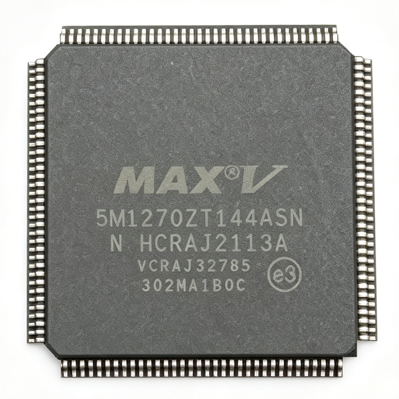
5M1270ZT144A5N - 980-Macro Cell MAX V CPLD, TQFP-144 | Intel
The Intel (formerly Altera) 5M1270ZT144A5N is a 980-macro-cell CPLD from the MAX V family, housed in a 144-pin TQFP (T144) package with 114 user I/Os and a maximum operating frequency of 201.1 MHz. The device operates from a 1.8 V core supply with on-chip voltage regulation supporting 1.8 V, 2.5 V, 3.3 V, and 5.0 V mixed-voltage I/O banks, and is built on a low-power non-volatile flash process that delivers zero in-system configuration time at power-up. A CPLD (Complex Programmable Logic Device) is a non-volatile programmable logic device that combines the instant-on behavior of a small PAL/GAL array with the logic density of an FPGA, typically used for glue logic, bus interfacing, power-up sequencing, and state-machine control. The MAX V family sits between discrete logic and high-density FPGAs in the programmable logic taxonomy: CPLD -> programmable logic -> logic IC -> integrated circuit -> semiconductor. Each macro cell includes a programmable AND/OR array plus a flip-flop, which the Quartus II / Quartus Prime toolset synthesizes from VHDL or Verilog. Key features include 980 macro cells (equivalent to ~2120 logic elements), 8 Kbits of user flash memory, a MultiVolt I/O interface, an on-chip oscillator, and IEEE 1149.1 JTAG boundary-scan support. The 5N speed grade combined with the 144-pin TQFP package targets designs that need medium-density logic, abundant I/O, and hand-solderable or socketed assembly rather than fine-pitch BGA mounting. Internal pull-up resistors and bus-hold circuitry simplify board design by eliminating external termination on many signal lines. The architecture is based on a non-volatile flash look-up table with CMOS process technology, providing instant-on capability and removing the need for an external boot PROM. The device supports in-system programmability via JTAG and is compatible with the Quartus II design software, which enables integration with both legacy schematic entry and modern HDL-based flows. Typical applications include I/O expansion and bus bridging for microcontrollers and SoCs, power-up and power-down sequencing for multi-rail systems, glue logic replacement for discrete 74-series gates, LED display driving, and protocol conversion (for example, SPI to parallel or UART to SPI). The TQFP-144 footprint also makes it suitable for educational platforms and rapid-prototyping boards where a socketed part is preferred over a BGA. When designing with this part, place 0.1 uF and 10 uF decoupling capacitors close to every VCCINT and VCCIO pin, and observe the multi-voltage I/O bank rules so that 5 V-tolerant inputs do not exceed absolute maximum ratings. Designers migrating from legacy MAX 7000 or MAX II parts should note that MAX V delivers up to 2x higher logic density per macro cell and adds user flash, but uses the same JTAG programming chain and pinout philosophy for backward-compatible boards. This page synthesizes verified distributor inventory, drop-in same-package alternatives drawn from the MAX V family, and practical design notes that go beyond the manufacturer datasheet table. Pricing is shown as of 2026-09-06 from DigiKey, Mouser, and Octopart.
5M1270ZT144C4N - MAX V CPLD, 980 Macrocells, 144-TQFP | Altera
The Altera (Intel) 5M1270ZT144C4N is a MAX V family Complex Programmable Logic Device (CPLD) providing 980 macrocells, 1270 logic elements, and 114 user I/O pins in a 144-pin TQFP package. Built on a low-power 0.18 um CMOS process, it delivers non-volatile Flash configuration with in-system programmability (ISP) via JTAG and operates from a 1.71 V to 1.89 V core supply. The device achieves pin-to-pin propagation delays of 8.1 ns and supports system frequencies up to 247.5 MHz, making it one of the highest-density members of the MAX V CPLD family. What is a CPLD? A Complex Programmable Logic Device is a non-volatile programmable logic IC that sits between simple glue-logic PALs/GALs and high-density FPGAs. CPLDs are typically used for system-level functions such as I/O expansion, interface bridging, power-up sequencing, bus decoding, and timing control - applications where fast, deterministic propagation delays and instant-on configuration are more important than the massive logic density of an FPGA. They occupy the middle of the programmable logic hierarchy: PAL/GAL -> CPLD -> FPGA. Key features of the 5M1270ZT144C4N include 980 macrocells distributed across 8 logic array blocks (LABs), 114 general-purpose I/Os with 3.3 V LVCMOS/LVTTL compatibility on user I/O banks, an internal oscillator, and user flash memory (UFM) blocks for non-volatile data storage. The device supports 1.8 V core operation with multi-voltage I/O support and consumes less than 100 mA typical quiescent current, making it suitable for power-sensitive designs. Architecturally, MAX V CPLDs use a non-volatile Flash-based configuration cell that eliminates the need for external boot PROMs and enables instant-on behavior at power-up. The 8.1 ns pin-to-pin tPD provides deterministic timing that is independent of design routing, which is critical for asynchronous interface bridging, reset distribution, and interrupt prioritization logic. Multi-voltage I/O banks support seamless interfacing with 1.8 V, 2.5 V, 3.3 V, and 5 V-tolerant signals. Typical applications include I/O expansion and level translation for microcontrollers, I2C/SPI/UART bus multiplexing, industrial control glue logic, LED display drivers, and any design requiring instant-on programmable logic without external boot memory. The 5M1270ZT144C4N is commonly specified in industrial automation, telecommunications equipment, and consumer electronics designs. When designing with this CPLD, ensure that the Quartus II or Intel Quartus Prime design tool is used for synthesis, placement, and programming file generation. The 144-pin TQFP package has a 22 mm x 22 mm body with 0.5 mm pitch, requiring standard surface-mount assembly techniques and adequate thermal relief for moderate-power designs. This page synthesizes distributor pricing, drop-in alternatives, and practical design notes not found in the manufacturer datasheet, giving engineers a single reference for sourcing and substituting the 5M1270ZT144C4N in existing designs.
5M1270ZT144C5N - MAX V CPLD 980 Macrocells 114 I/O TQFP-144 | Intel / Altera
The Intel / Altera 5M1270ZT144C5N is a MAX V series Complex Programmable Logic Device (CPLD) with 1270 logic elements (980 macrocells), housed in a 144-pin TQFP (T144) surface-mount package. It delivers a maximum internal operating frequency of 118.3 MHz, 6.2 ns pin-to-pin propagation delay, and integrates 114 user I/Os across four I/O banks with per-bank VCCIO support from 1.2 V to 3.3 V. The flash-based non-volatile configuration eliminates external boot memory and supports instant-on operation. Core voltage VCCINT operates from 1.71 V to 1.89 V. What is a CPLD? A Complex Programmable Logic Device is a non-volatile programmable logic IC that sits between simple glue-logic gates and high-density FPGAs in the programmable logic hierarchy: discrete logic -> SPLD (PAL/GAL) -> CPLD -> FPGA. CPLDs provide deterministic, low-latency combinational and registered logic with predictable timing, instant-on flash configuration, and high I/O count - ideal for I/O expansion, bus bridging, interface bridging, and power-up control functions. Compared with FPGAs, CPLDs offer lower power, smaller die area, and faster time-to-market for glue-logic tasks that do not need block RAM or DSP. Key features of the 5M1270ZT144C5N include 980 macrocells / 1270 logic elements, multi-voltage I/O support (LVCMOS, LVTTL, PCI up to 3.3 V, and 1.2 V to 3.3 V LVCMOS on JTAG pins), built-in JTAG (IEEE 1149.1) and in-system programmability via Altera Quartus II, and user flash memory (UFM) up to 8 Kbits for non-volatile user data. The device is rated for commercial 0 C to +85 C ambient operation. Architecturally, the MAX V family uses a classic LAB (Logic Array Block) macrocell fabric with a continuous FastTrack interconnect, giving predictable timing independent of design placement. The flash-based configuration cell is in-system programmable over JTAG and supports up to 100,000 program/erase cycles for design revision and field updates. Typical applications include industrial I/O expansion and level shifting, bus-bridging interfaces between processors and peripherals, power-up sequencing controllers, LED display drivers, and board-management controllers. The wide 114-I/O count makes it well suited to mid-density glue-logic consolidation where multiple discrete 74-series devices would otherwise be required. When designing with this device, ensure JTAG chain integrity by buffering TMS, TDI, TDO, and TCK lines; pull-ups are recommended on TCK per IEEE 1149.1. Decoupling VCCINT and VCCIO banks separately - the four I/O banks can run at independent voltages, so per-bank 0.1 uF ceramic decoupling is required. Configure unused I/Os as inputs with internal weak pull-up to minimize power. This page consolidates drop-in alternatives, distributor pricing, and design notes not found in the manufacturer datasheet alone, giving engineers a fast decision matrix for sourcing and replacement of MAX V CPLDs.
5M1270ZT144I5 - MAX V CPLD, 980 Macro Cells, 144-TQFP | Intel
The Intel (formerly Altera) 5M1270ZT144I5 is a MAX V family Complex Programmable Logic Device (CPLD) integrating 980 macro cells and 114 user I/Os in a 144-pin TQFP package. It operates from a 1.8V core supply with internal frequency support up to 201 MHz and 10 ns propagation delay, delivering low-power, instant-on programmable logic for glue-logic and I/O expansion roles. A CPLD (Complex Programmable Logic Device) is a non-volatile programmable logic device that sits in the system hierarchy between simple PLDs and full FPGAs. It provides fast, deterministic pin-to-pin combinatorial and sequential logic with on-chip flash configuration, ideal for bus decoding, power sequencing, interface bridging, and control-plane state machines. The MAX V family is built on a 0.18 µm flash-based process, retaining configuration without external boot memory and offering multi-volt I/O support from 1.2V to 3.3V. Key features of the 5M1270ZT144I5 include 980 logic elements (macro cells) split across 8 logic array blocks (LABs), 114 user I/Os, 1.8V core operation, in-system programmability via JTAG, and 8 Kbits of user flash memory. The 144-pin TQFP (22 × 22 mm, 0.5 mm pitch) industrial-grade package supports –40 °C to +100 °C ambient operation, and the device is RoHS-compliant for surface-mount assembly. Architecturally, the MAX V CPLD uses a classic AND-OR PLA fabric with each macro cell containing a flip-flop, programmable carry chain, and wide input LUTs. The 201 MHz internal frequency and 10 ns tPD support high-speed glue logic such as PCIe side-band control, memory controller address decoding, and high-speed bus arbitration where deterministic latency is mandatory. Typical applications include industrial control I/O expansion, automotive infotainment bus bridging, telecom line-card glue logic, and white-goods motor-control boards. Designers also deploy it as a low-cost alternative to small FPGAs where non-volatility and instant-on behavior eliminate the need for external boot PROMs. When designing with the 5M1270ZT144I5, pay attention to JTAG chain ordering when the device shares a programming interface with other Intel/Altera devices, and reserve at least 4 pins for JTAG (TCK, TMS, TDI, TDO). Decoupling follows standard high-speed logic practice: place 100 nF ceramics at every VCCIO bank and a 10 µF bulk capacitor near the core supply pin. This page synthesizes distributor pricing, drop-in same-family alternatives, and practical design notes not found in the bare datasheet. Pricing references are as of 2026-09-06 from authorized distributors.
5M1270ZT144I5N - MAX V CPLD, 980 LE, 144-TQFP | Intel / Altera
The Intel / Altera (formerly Altera) 5M1270ZT144I5N is a MAX V family Complex Programmable Logic Device (CPLD) that delivers 980 macro cells, 212 user I/O pins, and a 201.1 MHz internal operating frequency in a 144-pin TQFP package. It is built on a low-power, non-volatile flash process that retains configuration without an external boot PROM, and operates from a 1.8 V core supply with 1.2 V/3.3 V multi-voltage I/O support for direct interface to legacy and modern logic families. A CPLD (Complex Programmable Logic Device) is a non-volatile programmable logic device that combines multiple PAL/GAL-style macrocells with a centralized interconnect fabric. In the broader programmable logic hierarchy it sits below FPGAs in density and above simple SPLDs in logic capacity, and is widely used as glue logic, interface bridges, and power-up controllers where instant-on deterministic behavior is required. The MAX V family uses a flash-based configuration cell, so the device is live within microseconds of power-up rather than milliseconds, which differentiates it from SRAM-based FPGAs that must load bitstreams at every boot. Key features of the 5M1270ZT144I5N include 980 logic elements (LEs), 8 Kbits of user flash memory, on-chip voltage regulation supporting 1.8 V to 3.3 V I/O standards, JTAG (IEEE 1149.1) and in-system programmability via the Altera/Intel Quartus toolchain, and an industrial operating temperature range of -40C to +100C (I-temp grade, indicated by the 'I' in the part number). The 144-pin TQFP package provides a 0.5 mm pitch and supports surface-mount assembly with standard reflow profiles, making it suitable for high-volume PCB manufacturing. From an architecture standpoint, the 5M1270ZT144I5N uses a Logic Array Block (LAB) structure with 980 macrocells distributed across multiple LABs, each containing 16 macrocells. The non-volatile flash configuration makes the device suitable for safety-critical boot logic, since configuration cannot be lost due to brown-outs or in-rush transients. Combined with deterministic 1.5 ns pin-to-pin propagation delays through the central switch matrix, the part is well suited to high-speed glue logic between processors, memory, and peripherals. Typical applications for the 5M1270ZT144I5N include I/O expansion and level shifting in industrial controllers, address decoding and bus glue logic for legacy 5 V and 3.3 V microprocessor systems, power-up sequencing and supervisory logic, custom peripheral interfaces in embedded designs, and LED display or motor-control timing logic. The combination of low power, instant-on behavior, and high I/O count also makes it attractive as a cost-effective bridge between processors and slow-speed peripherals. When designing with this part, follow Intel/Altera's Quartus II or Quartus Prime power estimation and pin assignment guidelines carefully: the 144-pin TQFP has a maximum of 212 usable I/O pins, so high-fanout designs should budget for the JTAG chain and global clock pins before allocating GPIO. Decoupling should follow the reference schematic with 0.1 uF and 10 uF capacitors placed within 100 mils of each supply pin to keep the internal 1.8 V regulator stable under dynamic load. This page synthesizes distributor pricing, drop-in alternatives in the same 144-TQFP footprint, and practical Quartus design notes not found in the standalone datasheet, giving procurement and engineering teams a single decision-ready reference.

5M160ZE64A5N - 128 Macro Cell MAX V CPLD, 118.3MHz, 64-EQFP | Altera
The Altera 5M160ZE64A5N is a 128-macro-cell, low-power, non-volatile CPLD from the MAX V family, housed in a 64-pin EQFP (exposed-pad QFP) package. It supports up to 118.3 MHz internal operation with a 7.5 ns pin-to-pin propagation delay, runs from a 1.8 V core supply with 3.3 V or 2.5 V I/O support, and is qualified to the AEC-Q100 automotive standard for harsh-environment designs. A CPLD (Complex Programmable Logic Device) is a non-volatile programmable logic IC that uses flash-backed macro cells and a fixed AND/OR fabric to implement glue logic, interface bridges, and state machines. Compared with SRAM-based FPGAs, CPLDs offer instant-on configuration (no external boot device), deterministic timing, and excellent fit for bus decoding, power-sequencing, and LED/display driving. The MAX V family specifically targets low standby current and pin-rich I/O configurations. Key features include 128 macro cells (160 logic elements), 54 user I/O pins, 8 Kbits of user flash memory, an internal oscillator, JTAG (IEEE 1149.1) boundary-scan support, and in-system programmability via JTAG or Altera/Altera-Quartus. The non-volatile flash fabric eliminates the need for a separate boot PROM and supports >10,000 program/erase cycles, making the device well suited for factory-floor reprogramming and field updates. Architecturally, the 5M160ZE64A5N uses Altera's classic LAB (Logic Array Block) topology with 16 macro cells per LAB, an interconnect matrix, and per-pin I/O registers with programmable slew rate, bus-hold, pull-up, and open-drain options. The exposed thermal pad on the EQFP-64 package keeps junction temperatures manageable at industrial -40C to +125C ambient ranges. Typical applications include I/O expansion and bus bridging in industrial controllers, power-management sequencing for FPGA-based boards, automotive body-electronics modules, motor-control glue logic, and legacy-interface translation (PCI/ISA to modern serial buses). The 64-EQFP footprint offers a balance of I/O count and board-level manufacturability for both hand-soldered prototypes and high-volume reflow lines. When designing with this part, observe the recommended operating range (1.71 V to 1.89 V for VCCINT) and use the JTAG chain for ISP. Plan decoupling carefully - place 0.1 uF ceramics close to every supply pin and bulk tantalum or polymer caps near the EQFP exposed pad to manage in-rush during flash programming. This page synthesizes distributor pricing, AEC-Q100 variants, drop-in same-package alternatives, and practical design notes for the MAX V 5M160ZE64A5N that are not collated in the manufacturer datasheet alone.
5M160ZE64C4N - MAX V CPLD 128 Macro 54 IOs EQFP-64 | Intel
The Intel 5M160ZE64C4N is a member of the MAX V family of low-cost, low-power Complex Programmable Logic Devices (CPLDs) housed in a 64-pin plastic Enhanced Quad Flat Pack (EQFP-64) package with 54 user I/Os. It integrates 128 Logic Elements (LEs) / 128 macrocells, 8 Kbits of user flash memory, and a non-volatile flash-based configuration cell that enables instant-on operation without external boot devices. A CPLD (Complex Programmable Logic Device) is a non-volatile programmable logic device that combines multiple PLA-style macrocells and a global interconnect matrix into a single chip, offering deterministic timing, single-chip operation, and infinite reconfigurability. The MAX V family targets glue-logic, bus-interface, I/O expansion, and power-sequencing roles where ASICs would be uneconomical and FPGAs would be over-specified; within Intel's programmable-logic taxonomy, MAX V sits below Cyclone FPGAs but above discrete 74-series glue logic. Key features include an internal oscillator (3.3/5.0 V tolerant), 1.8 V/2.5 V/3.3 V MultiVolt I/O support, JTAG and ISP interfaces, and IEEE 1149.1 boundary-scan support. The device operates from a 1.71 V core supply with I/O banks supporting LVTTL, LVCMOS, PCI, and SSTL-2/3 standards. Per the Intel MAX V datasheet, the 'C4N' speed grade corresponds to tPD1 (pin-to-pin) of approximately 4.0 ns worst-case over commercial 0 C to 85 C conditions, while 'Z' denotes the 1.8 V core variant. Typical applications include bus-interface bridging, I/O expansion for microcontrollers without sufficient pins, power-up/down sequencing in multi-rail systems, address decoding for memory mapped peripherals, and state-machine controllers in industrial control. The flash-backed configuration eliminates the boot PROM that larger FPGAs require, simplifying BOM and reducing board area. When designing, ensure that all JTAG pins (TCK/TMS/TDO/TDI) are pulled or terminated correctly and that the E64 exposed pad is soldered to a clean ground plane for thermal dissipation. Quartus II / Quartus Prime support provides compilation, simulation and in-system programming flows.
5M160ZE64C5 - MAX V CPLD, 160 LEs, 64-EQFP | Intel (Altera)
The Intel (Altera) 5M160ZE64C5 is a MAX V family Complex Programmable Logic Device (CPLD) with 160 Logic Elements (LEs), 128 macrocells of Flash memory, and 54 user I/Os, housed in a 64-pin plastic Enhanced QFP (EQFP-64) package measuring 9x9 mm with 0.4 mm pitch. The device operates at an internal frequency up to 184 MHz with a propagation delay of 7.9 ns and supports commercial temperature grading (C suffix). A CPLD (Complex Programmable Logic Device) is a non-volatile programmable logic device that sits in the broader programmable logic hierarchy between simple PLDs (SPLDs) and FPGAs. CPLDs use a deterministic interconnect fabric and Flash-based configuration memory to provide instant-on behavior at power-up, making them ideal for glue logic, bus interfacing, power-up sequencing, and state-machine control. The MAX V family specifically targets low-cost, low-power applications by integrating a Flash memory block and eliminating external configuration devices. Key features of the 5M160ZE64C5 include 7.5 ns pin-to-pin logic delay (tPD), 118.3 MHz maximum internal frequency, 1.8 V core voltage (Z designation), 3.3 V or 2.5 V multi-voltage I/O support, in-system programmability (ISP) via JTAG, and 128 Kbits of user Flash memory (UFM) usable as general-purpose non-volatile storage. The device uses a 4-input look-up table (LUT) architecture with a global routing pool and supports IEEE 1149.1 boundary-scan testing. The 5M160ZE64C5 uses a non-volatile Flash configuration cell based on a 0.18 micrometer process, providing instant-on operation and unlimited reconfigurability without external boot memory. Its MultiVolt I/O banks allow mixed-voltage interfacing on the same die, simplifying PCB designs that need to bridge 3.3 V peripherals with 2.5 V or 1.8 V processors, while the built-in JTAG port enables in-circuit reconfiguration during prototyping and field upgrades. Typical applications include industrial control and glue logic, I/O expansion and bus bridging, power-up sequencing and supervisory logic, LED display drivers, and consumer electronics interface controllers. The instant-on Flash-based architecture is particularly useful in safety-critical or deterministic-latency paths where FPGAs would require boot time. When designing with this device, note the difference between commercial-grade (C5 suffix) and industrial-grade (I5 suffix) temperature ranges. Ensure JTAG chain integrity by buffering TMS/TCK signals when multiple devices share the chain, and respect the 1.8 V core supply ramp time recommended in the datasheet to avoid configuration corruption. This page synthesizes distributor pricing, drop-in same-package alternatives, and practical design notes not found on a single manufacturer datasheet view, including cross-brand Intel/Altera MAX V family cross-references and direct EQFP-64 pinout data for engineers evaluating the 5M160ZE64C5 against other 160-LE CPLDs.
5M160ZE64C5N - MAX V CPLD, 160 LE, 54 I/O, EQFP-64 | Intel
The Intel (formerly Altera) 5M160ZE64C5N is a low-power, non-volatile MAX V family Complex Programmable Logic Device (CPLD) integrating 160 Logic Elements, 128 macrocells, and 54 user I/O pins in a 64-pin EQFP package with an exposed thermal pad. It supports a maximum internal operating frequency of 118.3 MHz (fMAX) and is built on a 0.18 µm Flash-based process that delivers instant-on, non-volatile configuration without external boot memory. The device operates from a single 1.8 V core supply and supports JTAG (IEEE 1149.1) and in-system programmability via Altera/Quartus design tools. A CPLD (Complex Programmable Logic Device) is a non-volatile programmable logic device that sits in the digital hierarchy between discrete 74-series glue logic and larger FPGAs. It belongs to the broader family of programmable logic devices (PLDs) and is commonly used for I/O expansion, bus bridging, power-up sequencing, and address decoding in cost-sensitive designs. Within the system hierarchy: CPLD -> PLD -> programmable logic -> digital semiconductor. MAX V devices specifically target low standby power (~25 µA typical), 1.8 V operation, and small footprint packages - bridging the gap between discrete logic and full FPGAs. Key features of the 5M160ZE64C5N include 160 Logic Elements (LE), 8 Kbits of Flash memory, 1.4 ns pin-to-pin logic delay (tPD), 8.5 ns maximum frequency (fMAX for logic, per datasheet), user flash memory block, JTAG boundary-scan test support, and an internal oscillator. The exposed-pad EQFP-64 package provides a low thermal resistance path to PCB copper for heat removal in industrial environments. The device uses a non-volatile Flash configuration cell, eliminating external configuration PROM. Its multi-voltage I/O bank (VCCIO) supports 1.5 V, 1.8 V, 2.5 V, 3.3 V, and LVCMOS/LVTTL signaling, allowing direct interface to modern processors, microcontrollers, ASICs, and legacy 5 V-tolerant busses (via resistor networks). This makes it ideal for glue-logic consolidation, peripheral I/O expansion, and bus translation tasks. Typical applications include industrial control logic, I/O expansion for microcontrollers and SoCs, bus interface bridging (e.g., SPI to parallel, I2C to GPIO), power-sequencer / supervisory logic, and LED / display driving in consumer and embedded products. The exposed pad (E64) ensures reliable operation across commercial temperature grades. When designing with this part, observe Quartus II / Quartus Prime pin assignment rules and connect the exposed pad to a solid ground plane for thermal relief. Use the Quartus PowerPlay Early Power Estimator to model I/O toggle power before PCB layout. Verify all unused pins are configured per the MAX V pin-connection guidelines. This page synthesizes distributor stock, drop-in same-package alternatives, and engineering design notes not found in a single source - including a Package row in the comparison table to confirm pin-to-pin compatibility.
5M160ZE64I4N - MAX V CPLD, 64-Pin EQFP | Intel
Intel 5M160ZE64I4N is a low-cost, low-power MAX V complex programmable logic device in a 64-pin EQFP package. The verified source identifies the MAX V device family and describes the part as a CPLD offering greater density and I/O capacity per footprint than other CPLDs. Exact logic-element count, operating-voltage value, propagation delay, user-I/O count, and temperature-range value are not included in the supplied verified data, so those parameters remain explicitly unverified rather than inferred from the ordering code. A CPLD, or complex programmable logic device, is a semiconductor in the programmable-logic hierarchy between fixed-function integrated circuits and larger FPGAs. Its configurable architecture implements Boolean logic, state machines, interface bridging, control sequencing, and glue logic. A MAX V CPLD is normally designed for applications requiring deterministic programmable behavior, low power consumption, and fast development through HDL-based design. The “Z,” “E64,” “I4,” and “N” markings may encode device, package, temperature, and shipping options, but their precise meanings must be confirmed from the manufacturer’s ordering-code documentation. The principal verified feature is its position in the MAX V CPLD family. The available distributor information characterizes the family as low cost and low power while providing more density and I/Os per footprint than other CPLDs. That combination targets compact control and interface designs where board area, power budget, and logic integration matter. The part is supplied in a 64-pin EQFP package, making the land pattern, pin assignment, and package drawing essential pre-layout review items. Architecturally, a CPLD implements programmed digital behavior through configurable logic resources and a programmable interconnect network. Engineers can use it to consolidate multiple small logic devices, generate precise timing and control sequences, or adapt board-level interfaces late in development. Because supplied sources do not expose the exact MAX V architecture details, designers should consult the manufacturer handbook before estimating speed, power, logic capacity, or I/O utilization. Typical potential applications include industrial control logic, communications-interface adaptation, test equipment, embedded control, and compact systems requiring board-level glue logic. These are category-level use cases rather than guaranteed operating-condition claims. The device’s suitability for a specific design depends on the unverified electrical, timing, thermal, and I/O specifications in the manufacturer datasheet. A key design consideration is footprint compatibility. Although several 5M160ZE64 ordering variants exist, only parts with an identical 64-pin package, matching pinout, acceptable temperature grade, compatible electrical specifications, and verified timing behavior should be considered drop-in candidates. This page does not treat reel-code or ordering-code variants as substitutes without that engineering evidence. The information synthesized here combines the supplied distributor and manufacturer-source references, clearly separates verified attributes from missing specifications, and applies a strict evidence standard to pricing, lifecycle, and pin-to-pin alternative claims.
5M160ZE64I5 - MAX V CPLD, 160 LE, 54 I/O, EQFP-64 | Intel
The Intel (formerly Altera) 5M160ZE64I5 is a MAX V family Complex Programmable Logic Device (CPLD) housed in a 64-pin EQFP (Plastic EQFP, 9 x 9 mm, 0.40 mm pitch) package. The device integrates 160 Logic Elements, 54 user I/Os, and an internal flash configuration memory of 8 Kbits, delivering a maximum clock frequency of 118.3 MHz with a pin-to-pin tPD of 7.9 ns. The "ZE" speed/power grade targets the lowest static power tier of the MAX V family while preserving fast I/O timing. A CPLD (Complex Programmable Logic Device) is a non-volatile programmable logic device that sits between discrete glue logic and FPGAs in the programmable logic hierarchy. Like an FPGA, a CPLD provides reconfigurable combinational and sequential logic, but unlike most FPGAs it uses a non-volatile flash process, instant-on configuration, and a deterministic interconnect fabric with predictable timing. In the broader taxonomy, CPLD -> programmable logic device (PLD) -> logic IC -> integrated circuit -> semiconductor. Key features of the 5M160ZE64I5 include single 1.8 V core supply operation (VCCINT), multi-voltage I/O banks supporting 1.2 V to 3.3 V interfaces (VCCIO), built-in user flash memory block (UFM) up to 8 Kbits for non-volatile data storage, JTAG (IEEE 1149.1) and Altera-internal ISP interfaces, and a commercial-grade operating junction temperature range of -40C to +100C (industrial). The device also supports in-system programmability through the JTAG pins without removing the part from the board. The MAX V architecture combines a low-power process with a MultiVolt I/O structure, allowing the CPLD to interface directly with 1.5 V, 1.8 V, 2.5 V, and 3.3 V devices on the same PCB. Each Logic Element contains a 4-input look-up table, a programmable register, and a chainable carry/arithmetic structure. The non-volatile flash cell removes the need for a separate boot PROM and allows the device to begin user logic execution within microseconds of power-up. Typical applications of the 5M160ZE64I5 include bus-interface bridging (e.g., 8/16/32-bit local bus glue logic), I/O expansion and level translation, power-sequencer and reset-distribution logic, LED display driving and scan-control, industrial control boards, and low-density state-machine replacement of discrete 74-series logic. Its wide I/O voltage tolerance makes it useful as a mixed-voltage glue device between MCUs of different generations. When designing with the 5M160ZE64I5, ensure that VCCINT and VCCIO are decoupled with 0.1 uF and 1 uF ceramic capacitors placed close to the supply pins. The JTAG TCK frequency must stay below the device ISP limit when programming in-system, and unused I/O pins should be configured as outputs driving low to minimise power consumption. Designers migrating from older MAX II designs can reuse the same Quartus Prime II toolchain and JTAG chain. This page synthesizes distributor pricing, drop-in alternatives, and practical design notes not found in the manufacturer datasheet.
5M160ZE64I5N - 160 Logic Element MAX V CPLD | Intel | 64-EQFP
The Intel (formerly Altera) 5M160ZE64I5N is a low-power, non-volatile MAX V Complex Programmable Logic Device (CPLD) offering 160 Logic Elements (LEs), 128 macrocells, and 7.5 ns pin-to-pin logic delay, housed in a 64-pin EQFP (Exposed Pad Quad Flat Pack) package. The 'I' suffix indicates the industrial temperature grade of -40C to +100C, and the '5' speed grade places it in the standard performance tier of the MAX V family, while the 'N' indicates lead-free / Pb-free assembly. A CPLD (Complex Programmable Logic Device) is a non-volatile digital IC that contains multiple logic array blocks (LABs) interconnected by a programmable switch matrix. In the broader taxonomy, CPLDs sit below FPGAs in logic density but above discrete 74-series glue logic, providing instant-on configuration from on-chip flash, deterministic timing, and dozens to hundreds of I/O pins in a single chip - ideal for I/O expansion, bus bridging, power sequencing, and control logic in cost-sensitive embedded designs. Key features include 128 macrocells distributed across 4 logic array blocks, 4.0 Kbits of user flash memory for in-system custom configuration, 3.3 V or 2.5 V core operation with multi-voltage I/O banks (1.5 V / 1.8 V / 2.5 V / 3.3 V LVCMOS/LVTTL), and IEEE 1149.1 JTAG support via the TMS, TDI, TDO, and TCK pins. The device supports LVDS, RSDS, mini-LVDS, and LVPECL differential I/O via emulated pairs, and the MultiVolt core allows flexible interface to 1.5 V, 1.8 V, 3.3 V, and 5 V systems. Architecturally, the 5M160ZE64I5N uses a CMOS SRAM-based LUT fabric backed by non-volatile flash, giving instant-on behavior with no external configuration PROM. Each macrocell contains a programmable register that can be configured as D, T, JK, or SR flip-flop, with the logic array block switch matrix providing fast, deterministic signal propagation. This combination delivers the predictability engineers expect from a CPLD while keeping quiescent current around 25 microamps in standby. Typical applications include I/O expansion and level translation in industrial control boards, glue logic for microprocessors and DSPs, power-up sequencing for multi-rail systems, JTAG chain management, LED display driving, and general-purpose state-machine replacement. The wide I/O bank voltage support makes it especially useful as a bridge between legacy 5 V peripherals and modern 1.8 V / 3.3 V processors. When designing with this device, confirm that your Quartus II / Quartus Prime toolchain supports the MAX V device family (free Web Edition or licensed Subscription Edition). Pin assignment can be performed with the Pin Planner tool, and JTAG programming uses a USB-Blaster, ByteBlaster, or compatible cable. The exposed thermal pad on the EQFP package must be soldered to the PCB ground plane for proper thermal and electrical performance. This page synthesizes distributor pricing, drop-in alternatives within the MAX V family, and practical design notes not found in the manufacturer datasheet alone, giving engineers a single reference for sourcing, replacement, and application.
5M160ZM100A5N - MAX V CPLD, 128 Macrocells, 100-FBGA | Intel
The Intel (formerly Altera) 5M160ZM100A5N is a member of the MAX V family of low-power, non-volatile Complex Programmable Logic Devices (CPLDs) delivering 128 logic macrocells, 79 maximum user I/Os, and 8 Kbits of user flash memory in a 100-ball Fine-Pitch Ball Grid Array (Micro FBGA) measuring 6x6 mm with a 0.5 mm ball pitch. The device is built on a 0.18 µm CMOS flash process that supports in-system programmability through the IEEE 1532 / JTAG interface, enabling configuration to be retained without external memory. Per the MAX V family datasheet, the device operates from a 1.8 V core supply with internal voltage regulators accepting 1.71 V to 3.0 V on VCCINT-style rails, while I/O banks tolerate 1.2 V to 3.3 V LVCMOS/LVTTL signaling. A Complex Programmable Logic Device (CPLD) is a non-volatile programmable logic device that combines the deterministic timing of PAL/GAL architecture with on-chip flash configuration memory. In the broader programmable logic taxonomy, the MAX V family sits between small FPGAs (which offer higher logic density but require external configuration memory) and discrete logic gates (which offer no programmability). CPLDs are typically used for I/O expansion, bus bridging, power-up sequencing, and glue-logic tasks where instant-on behavior is required. Key features of the 5M160ZM100A5N include 118.3 MHz internal fMAX, 14 ns pin-to-pin propagation delay (industrial grade), 25 µA typical standby current, and integrated flash configuration storage. The device also supports MultiVolt I/O, in-system programmability (ISP), and a built-in 8 Kbit user flash memory block. The A5N speed grade and industrial temperature rating (-40 °C to +85 °C) make it well suited for industrial control and automotive-adjacent applications. Architecturally, the MAX V device uses a Logic Array Block (LAB) structure with 128 macrocells distributed across 4 Logic Array Blocks, each containing 16 macrocells. MultiCore architecture connects LABs through a programmable interconnect array (PIA), and the integrated flash memory holds both the configuration image and user-accessible flash sectors, eliminating the need for an external boot PROM. Typical applications include I/O expansion and level translation in industrial PLCs, glue logic in telecom baseband boards, power-sequencing controllers for FPGA-based SoCs, and bus-bridging interfaces between legacy microcontrollers and modern processors. The instant-on capability is particularly attractive for safety-critical systems requiring deterministic configuration at power-up. When designing with this device, ensure the JTAG chain respects the IEEE 1149.1 boundary-scan order and that VCCIO banks are properly decoupled with 0.1 µF and 10 µF capacitors placed close to the package balls. The internal flash programming voltage is generated on-chip; no external programming supply is required. This page synthesizes distributor pricing, drop-in alternatives, and practical design notes not found in the manufacturer datasheet alone.
5M160ZM100C4N - 128-Macrocell CPLD | Intel | Logic Control
Intel 5M160ZM100C4N is a 128-macrocell complex programmable logic device (CPLD) with a 7.5 ns propagation delay, 1.71 V to 1.89 V supply range, and a 100-pin micro FBGA package. It provides 79 user I/O pins in a compact 6 mm × 6 mm package with 0.50 mm ball pitch, making it suitable for digital control, interface bridging, and configurable glue-logic applications. The C4N ordering code is identified by distributor listings as a commercial-temperature device operating from 0 °C to +85 °C. A CPLD is a programmable logic device that combines nonvolatile configuration with a network of logic blocks, programmable interconnects, and I/O cells. Unlike a general-purpose FPGA, a CPLD generally provides predictable timing, fast configuration, and deterministic behavior for control and interface logic. It sits within the programmable-logic hierarchy between simple programmable logic devices and larger FPGAs, serving applications that need moderate logic density, rapid power-up, and board-level control without an external configuration memory. The key characteristics of the 5M160ZM100C4N are its 128 macrocells, 79 user I/Os, 1.71 V to 1.89 V operating supply, 7.5 ns propagation-delay specification, and 100-pin micro FBGA package. The 0.50 mm pitch supports dense board placement, while the commercial temperature range from 0 °C to +85 °C fits standard commercial electronics. Its flash-based programmable-logic classification is also listed by part distributors, supporting use in designs requiring reconfigurable digital control. The device is identified as an Altera MAX V-family CPLD by the supplied product listings. The verified sources describe a 6 mm × 6 mm, 0.50 mm-pitch MBGA-100 package and list 184 MHz internal frequency in one result, while another result identifies a 7.5 ns CPLD timing specification. The available data does not establish detailed I/O-bank voltages, configuration-interface timing, power-consumption values, or the complete package pin map, so those parameters remain unverified. Typical applications include industrial-control interfaces, communications and networking equipment, test and measurement systems, display-control logic, and board-level bus translation. The 128 macrocells provide moderate programmable capacity, while 79 user I/Os can support multiple control, status, and peripheral connections. The 7.5 ns timing figure makes the part relevant to conventional control-logic and interface designs, although exact design performance must be checked against the complete datasheet and timing model. When designing with the 5M160ZM100C4N, confirm the exact supply rail, temperature grade, I/O-bank requirements, configuration method, and package pinout before release. Because the supplied data identifies the package as 100-pin micro FBGA and lists a 0.50 mm pitch, PCB escape routing and assembly capability should be evaluated early. This page combines verified distributor specifications, source-traced sourcing information, and explicit data-needed markers where the provided evidence is insufficient.
5M160ZM100C5N - MAX V CPLD 128 Macro Cells 118.3MHz | Intel/Altera
The Intel/Altera (formerly Altera) 5M160ZM100C5N is a low-power, non-volatile MAX V Complex Programmable Logic Device (CPLD) with 128 macro cells (160 logic elements), 79 user I/Os, and a maximum internal frequency of 184 MHz (Fmax), housed in a 100-ball Micro FBGA (MBGA-100) package measuring 6 x 6 mm with 0.5 mm pitch. According to the FindIC summary of the Altera datasheet, the device operates from a 1.8 V core supply and supports the standard JTAG boundary-scan pins TMS, TDI, TDO, and TCK on Bank 1. A CPLD (Complex Programmable Logic Device) is a non-volatile, instant-on programmable logic device positioned in the hierarchy below FPGAs and above simple SPLDs/glue-logic ICs. CPLDs are widely used as I/O expansion, bus-interface bridging, power-up sequencers, and configuration controllers because they retain their configuration in flash, boot in microseconds, and offer deterministic timing. The MAX V family is Altera/Intel's smallest, lowest-cost CPLD line, typically selected for replacing dozens of discrete 74-series logic gates. Key specifications of the 5M160ZM100C5N include 128 macro cells (equivalent to 160 logic elements), 7.9 ns pin-to-pin propagation delay, 184 MHz internal performance, 1.8 V core VCCINT with multi-voltage VCCIO banks supporting 1.2 V, 1.5 V, 1.8 V, 2.5 V, 3.3 V, and LVCMOS/LVTTL I/O standards, plus an internal flash configuration memory with IEEE 1532 in-system programmability via JTAG. The MBGA-100 package provides 79 user I/Os in a compact 6 x 6 mm area. Architecturally, the MAX V CPLD combines a flash-based non-volatile configuration store with a classic macro-cell fabric of AND/OR arrays and product-term logic, eliminating the external boot PROM required by SRAM-based FPGAs. This makes 5M160ZM100C5N ideal for deterministic, instant-on glue logic in systems where SRAM-FPGA boot time is unacceptable. Typical applications include I/O expansion and bus bridging for microcontrollers, power-up/power-down sequencing in multi-rail systems, JTAG-controlled configuration of companion FPGAs, address decoding and chip-select generation, and replacement of multiple discrete 74-series TTL/CMOS gates. The 100-ball MBGA package suits space-constrained portable and embedded designs. When designing with this device, ensure that the VCCIO bank voltages match the driven/receiving logic; mixing 3.3 V peripherals with a 1.8 V bank will damage the I/O. Use the Altera/Intel Quartus II or Quartus Prime toolchain for synthesis, fitting, and JTAG programming. This page synthesizes distributor pricing from DigiKey/Mouser/LCSC, drop-in alternatives from the MAX V family, and practical Quartus toolchain notes not found in the bare datasheet.