Memory ICs
Subcategories
Products (482)
K9NUGY8R6B-BCQ0 - Samsung NAND Flash Memory | Samsung Electronics
The Samsung K9NUGY8R6B-BCQ0 is a NAND flash memory device from Samsung Electronics, part of the K9NUGY family of high-density non-volatile storage ICs used in solid-state storage, embedded systems, and consumer electronics. The device stores data in NAND flash memory cells and interfaces with a host controller through a standard asynchronous NAND interface, supporting page-based read, program, and block-erase operations under control of an external memory controller. NAND flash memory is a type of non-volatile storage technology that retains data without power. Within the memory hierarchy, it sits below DRAM in speed but offers far higher density and lower cost per bit, making it the dominant technology for SSDs, eMMC storage, USB drives, memory cards, and embedded flash. Samsung is one of the world's largest NAND flash manufacturers, and the K9 family of raw NAND devices has been an industry reference for decades. Key characteristics of this device class include high storage density per package, page-oriented program and erase operations, and a command/address/data multiplexed I/O interface. Error-correcting code (ECC) handling is performed by the host controller, as raw NAND devices do not manage ECC internally. Program and erase endurance, data retention, and block organization parameters should be confirmed from the official Samsung datasheet before design-in. Typical applications include solid-state drives, embedded storage modules, set-top boxes, digital televisions, network-attached storage, industrial data loggers, and removable media. In these systems the NAND device works alongside a flash controller that manages wear leveling, bad-block management, and ECC to deliver reliable long-term storage. Design considerations include power-supply decoupling on the VCC rail, careful PCB layout of the multiplexed address/data bus for signal integrity, and respect for tWB/tRR timing parameters during program operations. Ensure the host controller ECC strength matches the datasheet requirement for the device's NAND cell technology, as newer NAND generations require stronger correction capability. This page synthesizes cross-reference candidates, application guidance, and structured sourcing data in one place, adding value beyond the raw manufacturer datasheet listing.
K9PRGY8S7M - Samsung NAND Flash Memory IC | Samsung Electronics
The Samsung Electronics K9PRGY8S7M is a NAND flash memory integrated circuit belonging to Samsung's K9-series non-volatile memory lineup, supplied in a ball grid array (BGA) surface-mount package. Based on distributor listings (IC2IC, OMO Electronic, Alibaba), this device is cataloged as a Samsung NAND FLASH component and is actively traded on the open electronics market. NAND flash is a type of non-volatile storage technology that retains data without power. Within the memory hierarchy, NAND flash sits below DRAM in speed but offers far higher density and lower cost per bit, making it the backbone of SSDs, eMMC modules, USB drives, memory cards, and embedded storage. NAND cells are arranged in series, which reduces die area and enables the multi-gigabit capacities required by modern consumer, industrial, and automotive systems. Samsung is one of the world's leading NAND producers, with its 3D V-NAND technology stacking cells vertically to increase density further. Key characteristics of the K9-series include page-based program and block-based erase operations, asynchronous or toggled-mode interfaces, and internal ECC support on newer generations. Exact density, organization, page size, block size, and interface speed for this specific ordering code are not published in the retrieved web data and must be confirmed from the official Samsung datasheet. Typical applications for this class of device include embedded storage in set-top boxes, smart TVs, industrial controllers, networking equipment, and solid-state drive assemblies where a raw NAND device is managed by a host controller or firmware layer such as FTL (Flash Translation Layer). Design teams should confirm the exact package outline, ball map, supply voltage, and timing parameters against the Samsung datasheet before layout, since K9-series ordering codes encode density, configuration, and speed grade variations. Note that one distributor listing (OMO Electronic) attributes the MPN to BURNDY, which appears to be an indexing error given the K9 prefix and multiple corroborating NAND FLASH listings for Samsung. This page synthesizes open-market sourcing data, lifecycle status, and alternative-part guidance not consolidated on any single distributor page.
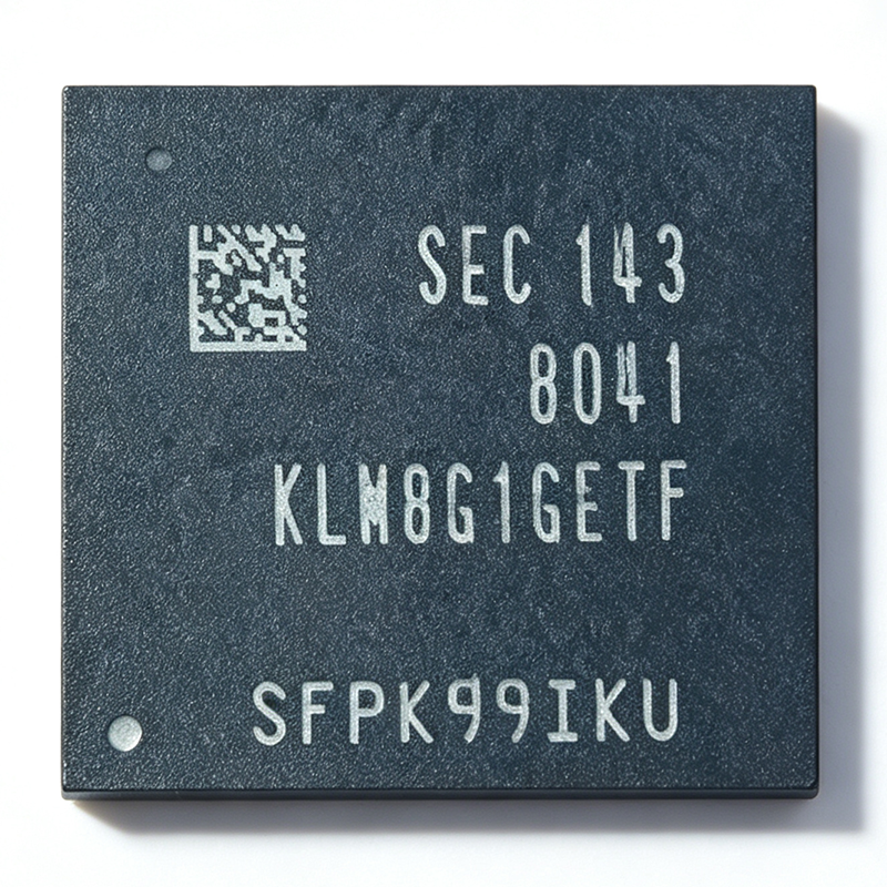
KLM8G1GETF-B041 - 8GB eMMC 5.1 Flash, 153-FBGA | Samsung
The Samsung KLM8G1GETF-B041 is an 8 GB (64 Gbit) eMMC 5.1 embedded flash storage device with MLC NAND, a 3V VDDF (NAND) supply, 1.8V/3V dual VCCQ supply, and a 153-pin FBGA package rated from -25C to +85C. An eMMC (embedded MultiMediaCard) is an embedded flash storage solution that integrates NAND flash die and a standard MMC controller in a single BGA package. It sits within the memory hierarchy as non-volatile embedded storage, managed through the JEDEC-standard MMC protocol v5.1, which presents a simple read/write register interface to the host processor instead of raw NAND management. Key features include eMMC 5.1 specification compatibility, built-in wear leveling, bad block management, ECC error correction, a hardware reset function, and secure write protection. Because the controller handles flash management internally, host software complexity is dramatically reduced compared with raw NAND. Technically, the device exposes a x1 or x4-bit or x8-bit data bus operating under MMC protocol v5.1, with VDDF at 3V for the NAND area and VCCQ at 1.8V or 3V for the interface. Samsung positions its eMMC eSTORAGE family as offering superior power efficiency and fast speed for slim mobile designs. The integrated controller performs erase management, wear leveling, and error correction transparently. Typical applications include smartphone and tablet main storage, smart home and IoT hubs, industrial HMI and data loggers, set-top boxes, and automotive infotainment head units. The 153-FBGA footprint and industry-standard interface allow drop-in swap between compliant 8GB eMMC 5.1 parts. Design consideration: verify the exact FBGA ball-map suffix, because suffix digits such as -B041 versus -B001 can encode different ball grid arrays, making physically incompatible parts that look identical on paper. This page synthesizes distributor pricing, drop-in alternative analysis, lifecycle alerts, and practical migration notes not found in the Samsung datasheet.
M25P16-VMF3PB - 16Mbit SPI NOR Flash 75MHz | Micron
The Micron Technology M25P16-VMF3PB is a 16 Mbit (2 Mb x 8) serial NOR Flash memory operating on an SPI-compatible bus at clock frequencies up to 75 MHz, supplied at 2.7 V to 3.6 V in a 16-pin SOP2 (16-SO) surface-mount package rated for -40 C to +125 C automotive temperature ranges. Serial NOR Flash is a non-volatile memory category that stores code and data in a NOR array architecture, allowing random access to any address through a simple serial peripheral interface (SPI). In the system memory hierarchy, it sits alongside parallel NOR and NAND Flash as a code-storage device, and is a direct descendant of the Numonyx/ST M25P family later acquired into the Micron portfolio. Compared with parallel Flash, SPI NOR reduces pin count, board area, and controller I/O requirements, which is why it dominates boot-code and firmware-storage roles in embedded designs. Key features of the M25P16-VMF3PB include its 75 MHz maximum clock frequency for fast code shadowing and XIP-style access, 2 Mb x 8 organization with 32 sectors of 64 Kbyte each (4 Kbyte subsector granularity via standard erase commands), advanced write-protection mechanisms, and deep power-down mode for minimum standby consumption. The automotive-grade suffix (PB, extended temperature) supports designs qualified to demanding environmental requirements. Architecturally, the device executes a standard SPI command set: READ and FAST_READ for data retrieval, PAGE PROGRAM for 256-byte page writes, SECTOR ERASE and BULK ERASE for content management, plus status-register and write-protect commands. The dedicated HOLD pin pauses serial communication without releasing the bus, and a hardware reset pin (S_RST on the 16-pin package) allows recovery of the serial interface. Typical applications include boot firmware storage for DSPs and microcontrollers, FPGA configuration bitstreams, parameter and calibration data storage in automotive modules, industrial drives, and set-top-box platforms. When designing with this device, verify hold times at the full 75 MHz clock and decouple VCC with 100 nF close to the supply pin; the 16-SOP2 footprint is wider than the 8-SO variant, so confirm the land pattern before second-sourcing. This page synthesizes distributor pricing, verified drop-in alternatives, and practical design notes not found in the manufacturer datasheet.
M25P16-VMF3TPB - 16Mb SPI NOR Flash 75MHz | Micron
The Micron M25P16-VMF3TPB is a 16Mb (2Mb x 8) serial NOR Flash memory with an SPI-compatible bus interface, up to 75 MHz clock support, and a 2.7V to 3.6V supply range, housed in a 16-pin SOIC wide-body (SO16W, 300 mil) package with -40C to +125C operation. Serial NOR Flash is a nonvolatile memory that stores code and data and is read over a simple four-wire SPI bus (chip select S, serial clock C, serial data input D, and serial data output Q). In the embedded-systems hierarchy it sits below parallel NOR and DRAM in bandwidth but above I2C EEPROMs in speed and density, making it the de facto standard for boot-code storage in microcontrollers, DSPs, and FPGAs. Key features of the M25P16 include 75 MHz SPI read operation, fast page programming (256-byte pages) and sector erase (64 KB sectors) with block protection, 15 ns clock-to-output access timing, and advanced write-protection mechanisms including status-register and hardware write protect. The VMF3 ordering option denotes the wide 16-pin SO package, RoHS-compliant lead-free construction, and Tape & Reel delivery, with the TP suffix indicating the shipping format. Architecturally, the device is an SLC single-level-cell NOR array organized as 2M x 8 bits, with an internal state machine that executes Read, Fast Read, Page Program, Sector Erase, Bulk Erase, and Write Status Register commands. Micron assigned this part to its Product Longevity Program, which suits multi-year industrial deployments; however, Micron has since EOL'd low-density serial NOR families, so the Renesas-published conversion guide to Adesto FUSION/Standard Flash and the cross-brand equivalents below are relevant for new sourcing. Typical applications include FPGA/DSP boot configuration (for example SHARC DSP boot loaders), BIOS/firmware storage in networking equipment, parameter and calibration data logging in industrial drives, and set-top-box or display firmware storage. Design consideration: hold the HOLD pin high and tie WRITE PROTECT appropriately; use 100 nF decoupling at VCC and respect the deep power-down entry/exit timing to minimize standby current. This page synthesizes verified distributor data, drop-in same-package alternatives, and sourcing guidance for a part affected by Micron EOL - information not consolidated in the manufacturer datasheet.

M25P16-VMN3PB - 16Mb SPI NOR Flash 75MHz SOIC-8 | Micron
The Micron M25P16-VMN3PB is a 16 Mbit (2 M x 8) serial NOR Flash memory with a high-speed SPI-compatible bus, clocking up to 75 MHz, in an 8-pin SOIC (208-mil SO, SOP) package. It is rated for the automotive temperature grade of -40C to +125C and is covered by Micron's Product Longevity Program. Serial NOR Flash is a non-volatile memory category within the broader memory IC and semiconductor hierarchy. Unlike NAND Flash, NOR Flash allows random-access reads of individual bytes, making it the standard choice for firmware boot code storage in embedded systems, where the processor must execute or quickly fetch code directly from the memory array over an SPI bus. Key features of the M25P16 include 16,777,216 bits of SLC (single-level cell) NOR storage organized as 2,097,152 bytes x 8, a 75 MHz maximum SPI clock frequency, 100,000 program/erase cycles endurance, and advanced write-protection mechanisms. Page program and sector erase operations are supported with block-level protection for reliable code and data storage. Architecturally, the device uses a standard SPI interface with signals S (chip select), D (serial data input), Q (serial data output), and C (serial clock), plus WP# (hardware write protect) and HOLD# (pause communication without deselecting). The automotive temperature grade and Product Longevity Program membership make it suitable for long-lifecycle deployments where sourcing continuity matters. Typical applications include automotive modules, industrial controllers, embedded firmware boot storage, data logging, computing modules, and configuration storage for FPGAs and SoCs requiring dependable non-volatile code memory. Design tip: verify VCC decoupling and use hold operations carefully - releasing HOLD# mid-clock requires an edge on C to resume, so keep timing margins in multi-master SPI buses. This page adds distributor pricing tiers, drop-in alternative cross-references, and practical design notes not consolidated in the manufacturer datasheet.
M25P16-VMN3YPB - 16Mbit SPI NOR Flash 75MHz SOIC-8 | Micron
The Micron M25P16-VMN3YPB is a 16Mbit (2MB) serial NOR Flash memory with an SPI interface operating up to 75 MHz, supplied in an 8-pin SOIC (8-SO, 3.90 mm width) package with automotive temperature grade. It stores data as 16M x 1 bits and uses a standard SPI command set for read, page program, and sector erase operations. Serial NOR Flash is a nonvolatile memory category within the memory IC hierarchy (Flash memory -> NOR Flash -> serial/SPI NOR Flash -> nonvolatile semiconductor memory). Unlike parallel NOR devices, SPI NOR Flash uses a reduced pin count (8 pins) communicating over a clocked serial bus, which makes it ideal for storing boot code, firmware, and configuration data in space-constrained embedded systems. Key features of the M25P16-VMN3YPB include its 16Mbit density organized for x1 SPI access, a 75 MHz maximum clock frequency for fast code-shadowing reads, and an automotive temperature grade per distributor data (Partstack/Vyrian list Temperature Grade: AUTOMOTIVE), supporting -40C to +125C environments. The 8-SOIC footprint is industry-standard, easing second-source qualification. Architecturally, the device is organized into pages for programming and larger sectors for erase, with the standard Micron M25P family command set (READ, FAST_READ, PAGE PROGRAM, SECTOR ERASE, BULK ERASE, write protection via the /W pin, and /HOLD for bus suspension). This command compatibility is why the M25P16 is frequently cross-referenced by vendors such as STMicroelectronics and Winbond equivalents in the same SOIC-8 footprint. Typical applications include FPGA configuration bitstream storage, microcontroller boot firmware, automotive infotainment and body-control module code storage, LCD display panel parameter memory, and communication equipment configuration storage. The 75 MHz SPI clock supports fast boot-time readout where a quad interface is not required. Design consideration: verify the supply range and pin functions against the manufacturer datasheet before drop-in substitution; the /W (write-protect) and /HOLD pins must be driven correctly by the host, as not all competitor devices define identical hold behavior. This page synthesizes distributor pricing, stock data, drop-in alternatives, and practical design notes not found in a single datasheet, giving engineers a complete qualification-ready view of the M25P16-VMN3YPB.
M25P20-VMN3PB - 2Mbit SPI NOR Flash 75MHz SOIC-8 | Micron
The Micron M25P20-VMN3PB is a 2 Mbit (256 Kbyte) low-voltage serial NOR Flash memory with a 75 MHz SPI bus interface, housed in an 8-pin SOIC (SOP-8) package. It operates from a 2.7V to 3.6V single supply over a -40C to +125C temperature range. Serial NOR Flash is a nonvolatile memory category in which data is read, programmed, and erased over a serial peripheral interface (SPI) rather than a parallel bus. Within the memory hierarchy it sits under Flash memory -> NOR Flash -> serial/quad SPI memory, and is widely used for code storage (XIP), FPGA configuration, and parameter logging because it offers random-access-like byte readability, high reliability, and a minimal pin count. Key features of the M25P20 include a 2 Mbit organization (256 Kbytes, 4 sectors of 512 Kbit each, 256-byte pages), page program times of 0.8 ms typical for up to 256 bytes, sector erase of 0.6 s typical (512 Kbit), and bulk erase of 3 s typical. The 75 MHz SPI clock rate supports fast code fetch and configuration downloads. Write protect and hold functions are provided on dedicated pins for hardware data protection and bus sharing. The M25P20 uses Micron NOR Flash cell technology with a standard SPI command set (READ, FAST_READ, PAGE PROGRAM, SECTOR ERASE, BULK ERASE, WRITE ENABLE/DISABLE, READ STATUS), making it command-compatible with many industry-standard serial Flash devices and simplifying firmware reuse. The VMN3 package option is lead-free (Pb-free) and RoHS compliant, and the device supports an extended industrial temperature range. Typical applications include FPGA configuration bitstream storage, embedded microcontroller code and data storage, LCD panel and display controller firmware, networking equipment boot code, and industrial automation parameter storage. The small SOIC-8 footprint suits space-constrained boards. For design, keep SPI trace lengths short and use series termination near the source when operating at the full 75 MHz clock rate; decouple VCC with a 100 nF ceramic capacitor close to pin 8. This page synthesizes distributor pricing, verified drop-in alternatives, pinout data, and practical design notes not consolidated in the manufacturer datasheet.
M25P20-VMN3TPB - 2Mb SPI NOR Flash 75MHz SOIC-8 | Micron
The Micron M25P20-VMN3TPB is a 2 Mbit (256K x 8) low-voltage serial NOR Flash memory with a 75 MHz SPI-compatible bus interface, housed in an 8-pin SOIC (SO, 0.150 inch, 208 mil) package supplied in tape and reel. Operating from 2.3 V to 3.6 V (2.5 V/3.3 V supply class), it delivers page programming of up to 256 bytes in 0.8 ms typical and an 8 ns access time. Serial NOR Flash is a nonvolatile memory category that stores code and data electrically and reads them out over a serial peripheral interface (SPI). In the system memory hierarchy it sits below DRAM and parallel NOR: it holds firmware, boot code, configuration bitstreams, and calibration tables that must survive power loss, trading parallel bandwidth for a minimal pin count and tiny footprint. SPI NOR is the de facto standard for boot memory in microcontroller, FPGA, and SoC platforms. Key features of the M25P20 include 75 MHz clock support for high-performance read commands, 2 Mbit density organized as 4 sectors of 512 Kbit each, sector erase in 0.6 s typical and bulk erase in 3 s typical, and advanced write-protection mechanisms. The -40C to +125C operating range supports industrial and automotive-adjacent environments, and product longevity commitments apply. Architecturally, the device uses a single-level NOR cell array addressed via SPI commands, with write-enable latching, status register polling, and hardware/software protection schemes preventing accidental program or erase. The VMN3 speed grade runs the full 75 MHz command set over the industrial temperature range. Typical applications include FPGA configuration storage, boot code memory for embedded processors, parameter and calibration storage in industrial drives, and firmware storage in networking and consumer equipment. Design consideration: keep the SPI clock and data traces short, place a 0.1 uF decoupling capacitor directly at the VCC pin, and respect the hold and write-protect pin states during power ramp-up to prevent spurious writes. This page synthesizes distributor pricing, same-family drop-in alternatives, pinout, and practical design notes not consolidated in the manufacturer datasheet.
M25P32-VMW3GB - 32Mbit SPI NOR Flash 75MHz | Micron
The Micron M25P32-VMW3GB is a 32Mbit (4M x 8) serial NOR flash memory with a 75 MHz SPI bus interface, 3.0 V to 3.6 V supply voltage, and an 8-pin SOIC wide-body (VMW, 208-mil SOIC-8 W) package. It is AEC-Q100 qualified for automotive applications and supports page program, sector erase, and bulk erase operations with hardware and software write protection. Serial NOR flash is a nonvolatile memory category in which data is accessed byte-wise over a serial peripheral interface (SPI) rather than a wide parallel bus. Within the memory hierarchy - memory IC -> flash memory -> NOR flash -> serial SPI NOR flash - these devices trade raw bandwidth for dramatically reduced pin count, tiny board footprint, and low cost, which is why they are the de facto standard for storing boot code, firmware images, and configuration data in embedded systems. Key features of the M25P32-VMW3GB include the 75 MHz maximum SPI clock frequency for fast firmware downloads, a 256-byte page with typical 0.8 ms page programming time, uniform 64-Kbyte sectors with 64 sectors total, and a deep power-down mode that reduces standby current to approximately 1 microamp. The device supports SPI modes 0 and 3, operates from a single 3.3 V supply, and offers hardware write protection on the /WP pin plus block-level software protection. Architecturally, the M25P32 inherits the Numonyx/ST M25P family design later acquired by Micron, using floating-gate NOR cells with a state machine handling the standard SPI command set (READ, FAST_READ, PAGE PROGRAM, SECTOR ERASE, BULK ERASE, WRITE ENABLE/DISABLE, READ STATUS).JEDEC-standard 16-bit signatures allow electronic signature identification for programmer compatibility. Typical applications include BIOS/firmware storage in automotive ECUs, boot code for FPGAs and microcontrollers, configuration storage in industrial drives and set-top boxes, and parameter logging in network equipment. Its AEC-Q100 qualification makes it a preferred choice for automotive temperature environments. Design tip: use FAST_READ at 75 MHz only after verifying your PCB signal integrity; at high clock rates, keep traces short and add series termination on SCK. This page synthesizes distributor pricing, drop-in alternatives, and practical design notes not found in the manufacturer datasheet.

M25P40-VMB3TPB - 4Mb SPI NOR Flash 75MHz | Micron Technology
The Micron M25P40-VMB3TPB is a 4Mb (512Kb x 8) serial NOR flash memory with a high-speed SPI-compatible bus interface supporting clock frequencies up to 75MHz, a supply voltage range of 2.3V to 3.6V, and an operating temperature range of -40C to +125C, housed in an 8-pin UFDFPN (2x3 mm) ultra-thin fine-pitch package. A serial NOR flash memory is a nonvolatile storage device that retains code and data without power and is read byte-by-byte over a serial bus, most commonly SPI (Serial Peripheral Interface). In the system memory hierarchy, NOR flash sits alongside parallel NOR, NAND flash, and EEPROM as a class of nonvolatile memory ICs, and it is the dominant choice for storing boot code in embedded systems because it offers random-access read behavior and high reliability. Key features of the M25P40 include 4Mb density organized as 512Kb x 8, 75MHz SPI clock operation for fast code fetch, advanced write-protection mechanisms, a wide 2.3V to 3.6V single supply, and an extended -40C to +125C industrial temperature range. The 8-UFDFPN (2x3 mm) package saves board space versus SOIC-8, making it suitable for compact designs. Architecturally, the device is accessed by a standard SPI bus using chip-select (S#), serial clock (C), serial data input (D), and serial data output (Q) signals, with HOLD# for bus suspension and WP# for hardware write protection. Sector and bulk erase operations, page programming, and status-register-based software protection are managed through standard commands, and the write-protection scheme protects the entire memory or individual sectors against accidental programming. Typical applications include firmware and boot-code storage in industrial controllers, consumer electronics, networking equipment, set-top boxes, printers, and automotive-adjacent body electronics where a small, reliable, low-voltage code flash is required. The 125C rating supports harsh industrial environments. When designing with this device, verify that your SPI controller supports the required 75MHz timing with adequate setup/hold margins, and budget erase/program times in your firmware update routines. Add proper decoupling on VCC and keep the clock line short to maintain signal integrity. This page synthesizes distributor pricing, drop-in alternatives, pinout data, and practical design notes not found in the manufacturer datasheet.
M25P40-VMN3PB - 4Mbit SPI NOR Flash 75MHz | Micron
The Micron M25P40-VMN3PB is a 4 Mbit (512K x 8) serial NOR Flash memory with a high-speed SPI-compatible bus interface up to 75 MHz, a 2.3 V to 3.6 V single supply range, and an operating temperature of -40C to +125C, housed in an 8-pin SOIC (3.90 mm width) package supplied in tubes. This industrial/automotive-temperature-grade member of the M25P40 family is covered by Micron's Product Longevity Program (program start date 5/4/2011). Serial NOR Flash is a nonvolatile memory category that stores code and data without power and is read through a serial peripheral interface (SPI) rather than a wide parallel bus. In the memory hierarchy it sits among low-density code-storage devices used for firmware boot, parameter storage, and FPGA/configuration loading, complementing DRAM (working memory) and high-density NAND Flash (mass storage). Key features include 4 Mbit of Flash organized x8, SPI bus compatibility (modes 0 and 3), 75 MHz clock operation for high-performance read commands, advanced write-protection mechanisms, and a low-voltage 2.3 V-3.6 V single supply. The -40C to +125C range and Product Longevity Program membership make it suitable for long-lifecycle embedded designs. Architecturally, the M25P40 divides the 4 Mbit array into uniform 64 Kbyte sectors that are independently erasable, with 256-byte page programming via the PAGE PROGRAM command. Standard SPI commands cover READ, FAST_READ, SECTOR ERASE, BULK ERASE, WRITE ENABLE, and status-register access; hardware write protect (WP#) and HOLD# pins support in-system control and bus sharing. Typical applications include boot-code and firmware storage in industrial controllers, configuration image storage for FPGAs and CPLDs, set-top boxes, networking line cards, and automotive modules operating across the full -40C to +125C range. Design consideration: note that Micron has announced end-of-life for low-density serial NOR products, so new designs should evaluate the alternatives listed on this page and qualify a second source early. This page synthesizes distributor pricing, drop-in alternatives, and EOL replacement guidance not found in the manufacturer datasheet.
M25P40-VMN3TPB - 4Mb SPI NOR Flash 75MHz | Micron
The Micron M25P40-VMN3TPB is a 4 Mbit (512K x 8) serial NOR Flash memory with a high-speed SPI-compatible bus interface supporting clock frequencies up to 75 MHz, operating from a single 2.3 V to 3.6 V supply in an 8-pin SOIC (SO, 3.90 mm width) package rated from -40C to +125C for automotive-grade environments. A serial NOR Flash memory is a nonvolatile semiconductor that stores code and data and reads it byte-by-byte over a serial bus. Within the memory hierarchy it sits in the code-storage class of the Flash memory family, below parallel NOR in pin count and above EEPROM in density, making it a standard boot-memory choice for embedded processors. Key features include 4 Mbit of Flash organized as 512K x 8 bits, a 75 MHz SPI bus interface for fast code execution (XIP), a 2.3 V to 3.6 V single supply for 3.3 V and low-voltage systems, advanced write-protection mechanisms, and sector/block erase architecture with page programming. Automotive temperature range -40C to +125C supports under-hood and industrial deployments. The device uses a standard SPI command set with read, fast-read, page program, sector erase, bulk erase, and write-protect commands. The HOLD# pin suspends serial communication without deselecting the device, and the W# pin provides hardware write protection, while status-register software protection guards against accidental program or erase operations. Typical applications include BIOS/code storage in automotive ECUs, boot memory for microcontrollers and FPGAs, configuration storage in industrial automation, and parameter storage in networking and consumer equipment where a small-footprint 8-SOIC nonvolatile memory is required. Design consideration: at 75 MHz keep SPI trace lengths short and match clock-to-data skew; use 10 k ohm pull-ups on HOLD# and W# to prevent accidental state changes during power-up. This page synthesizes distributor pricing, drop-in alternatives within the Micron M25P family, pinout data, and practical design notes not found in the manufacturer datasheet alone.
M25P64-VMF3PB - 64Mbit SPI NOR Flash 75MHz | Micron
The Micron Technology M25P64-VMF3PB is a 64 Mbit (8M x 8) serial NOR Flash memory with a 75 MHz SPI bus interface, operating from a 2.7 V to 3.6 V single supply voltage, housed in a 16-lead SOIC wide-body (16-SOP) surface-mount package. The -3P suffix denotes the automotive temperature grade, making this device suited to harsh-environment embedded designs. A serial NOR Flash memory is a non-volatile semiconductor memory that stores code and data and is accessed byte-by-byte over a serial peripheral interface (SPI). Within the memory hierarchy it sits alongside parallel NOR and serial NAND devices; because it offers random-access read capability, it is the dominant boot-memory choice for microcontrollers, FPGAs, and SoCs in the power management IC and semiconductor ecosystem. Key features of the M25P64 include 64 Mbit of Flash memory density, SPI-bus-compatible serial interface with clock rates up to 75 MHz, a 3 V class single supply (2.7 V to 3.6 V), sector and bulk erase operations, and a hardware write-protect pin. Automotive qualification and RoHS-compliant, lead-free packaging distinguish this variant for industrial and vehicular deployments. The device is organized as 8M words of 8 bits, with page-program and sector-erase commands defined in the M25P command set inherited from the Numonyx (STMicroelectronics) product line now owned by Micron. Page programming and fast read operations allow embedded bootloaders and configuration loaders to fetch FPGA bitstreams or MCU firmware efficiently over just four signal lines (S, C, D, Q), reducing pin count and PCB routing complexity versus parallel Flash. Typical applications include FPGA configuration storage (notably for Microsemi/Microchip RTAX and ProASIC3 radiation-tolerant and space-adjacent platforms), automotive ECU boot memory, and industrial firmware storage where non-volatile code retention and SPI simplicity are essential. For design, hold and write-protect timing must be respected during power sequencing, and the 75 MHz clock requires careful SPI signal-integrity layout with series termination on the clock line. This page synthesizes distributor pricing, drop-in alternatives, and practical design notes not found in the manufacturer datasheet.
M25P64-VMF3TPB - 64Mbit SPI NOR Flash 75MHz | Micron
The Micron Technology M25P64-VMF3TPB is a 64 Mbit (8M x 8) serial NOR Flash memory with an SPI-compatible bus interface, a 75 MHz maximum clock frequency, and a 3.0 V (2.7 V to 3.6 V) single supply, housed in a 16-pin wide-body SOIC (16-SOIC W, 7.50 mm / 300 mil body, tape and reel packaging). A serial NOR Flash memory is a non-volatile memory device that stores code and data while retaining contents without power, and is accessed byte-by-byte over a serial interface. In the memory hierarchy, NOR Flash sits alongside NAND Flash and EEPROM within the non-volatile memory family; unlike NAND, NOR supports direct random access to any address, which makes it the standard choice for direct code execution (XIP) of bootloaders and firmware in embedded systems. Key features include the 64 Mbit density organized as 8,388,608 bytes, SPI Mode 0 and Mode 3 operation at up to 75 MHz, hardware and software write-protection mechanisms (block protect and status register protection), sector erase and bulk erase instructions, and an automotive temperature grade suitable for -40C to +85C (and beyond, per grade coding) environments. The HOLD pin suspends serial communication without deselecting the device, useful in multi-slave SPI buses shared with real-time tasks. Architecturally, the M25P64 family uses a page-program architecture: data is programmed page-by-page into a buffer and then written to the array, with erase granularity at sector level. The 75 MHz SPI clock, combined with fast read and fast read dual-output style throughput, keeps boot times short for large firmware images, while the 8 ns access-time class reflects the internal read latency of the array. Typical applications include automotive ECU code and calibration storage, FPGA configuration boot memories in industrial and communications equipment, and firmware storage in set-top boxes, networking line cards, and telemetry modules where reliability and long-term availability matter. Design consideration: keep the SPI trace lengths short and add a 100 nF decoupling capacitor directly across VCC and GND; ensure the HOLD and WRITE PROTECT pins are actively driven to avoid floating-pin command corruption during power ramps. This page synthesizes distributor pricing and stock references, verified cross-references, and practical drop-in alternative analysis not consolidated in the manufacturer datasheet.
M25P80-VMN3TPB - 8Mbit SPI NOR Flash 75MHz SOIC-8 | Micron
The Micron M25P80-VMN3TPB is an 8Mbit (1M x 8) serial NOR Flash memory device with advanced write-protection mechanisms, accessed through a high-speed SPI-compatible bus, housed in an 8-pin SOIC (3.90mm width) package. It operates from a single 2.7V to 3.6V supply and supports clock frequencies up to 75 MHz. Serial NOR Flash is a non-volatile memory category within the broader Flash memory hierarchy (memory IC -> Flash memory -> NOR Flash -> serial SPI NOR Flash). Unlike parallel Flash, serial NOR uses a reduced pin count SPI interface, trading some bandwidth for board space, simplicity, and lower cost, which makes it the dominant choice for code storage in embedded systems. Key features include the 75 MHz maximum clock rate, page programming of up to 256 bytes in 0.64 ms typical, sector erase capability, and hardware and software write protection. The JEDEC-standard SPI command set and dedicated write-protect and hold pins simplify integration with virtually any microcontroller with an SPI peripheral. Architecturally, the device is organized as 16 sectors of 64 KB (1 Mbyte total), with page program and bulk/sector erase commands managed by an internal state machine. Supply range of 2.7V to 3.6V makes it compatible with standard 3.3V logic rails, and the hold pin allows the serial bus to be paused without deselecting the device. Typical applications include boot code and firmware storage for microcontrollers and FPGAs, parameter and calibration data storage in industrial equipment, and configuration memory in networking and consumer electronics. The SPI interface and small SOIC-8 footprint fit space-constrained embedded designs. Design consideration: honor the sector erase before page program requirement - the M25P80 can only program bits from 1 to 0, so software must erase (setting bits back to 1) at 64 KB sector granularity before rewriting, which influences firmware update layout. This page synthesizes distributor pricing, drop-in alternatives, cross-reference data, and practical design notes not found in the manufacturer datasheet.
M25PX80-VMN3TPB - 8Mb SPI NOR Flash 75MHz | Micron
The Micron Technology M25PX80-VMN3TPB is an 8 Mbit (1 M x 8) serial NOR Flash memory device with an SPI-compatible bus operating at up to 75 MHz, a 2.7 V to 3.6 V supply range, and an 8-pin SOIC (3.90 mm width) surface-mount package. Serial NOR Flash is a nonvolatile memory category that stores code and data without power, accessed over a reduced-pin-count SPI bus (chip select, serial clock, data-in, data-out). In the memory hierarchy it sits alongside parallel NOR and NAND Flash: NOR offers fast random read access ideal for execute-in-place (XIP) code storage, while the SPI interface reduces pin count, board area, and cost compared with parallel devices. Key features of the M25PX80 include the 75 MHz maximum SPI clock, dual input/output read commands that double transfer bandwidth for read and program operations, and advanced write-protection mechanisms documented in the M25PX80 datasheet. The device supports block and sector erase architectures typical of the M25PX family, with a 3V/3.3V operating voltage class suited to embedded processors, microcontrollers, and FPGA configuration loads. Architecturally, the M25PX80 uses a single-die NOR array with an SPI command set compatible with the widely deployed M25P family, adding enhanced programming performance and enhanced protection features. The VMN3 suffix denotes the 8-SOIC 150-mil package in tape-and-reel packing; the PB suffix indicates automotive temperature and quality flow, and the device is listed as AEC-Q100 qualified on Arrow.com. Typical applications include FPGA boot/configuration storage, MCU code and parameter storage in industrial controls, set-top boxes, networking line cards, and automotive body/comfort modules where a compact 8-pin footprint and Q-qualified flow are required. Design consideration: because the part is reported obsolete, new designs should plan a second source or footprint-compatible successor; verify hold and write-protect pin usage, as external pull-ups on HOLD# and W# are required when these functions are not actively driven. This page synthesizes distributor pricing, drop-in alternatives, lifecycle status, and practical design notes not found in the manufacturer datasheet.
M29DW323DB70N3E - 32Mb NOR Flash 70ns 48-TSOP | Micron
The Micron Technology M29DW323DB70N3E is a 32Mbit (4M x 8 or 2M x 16) 3V parallel NOR Flash memory with a 70 ns access time, housed in a 48-pin TSOP I (Type I) surface-mount package rated from -40C to +125C. Parallel NOR Flash is a nonvolatile memory technology organized in random-access addressable banks, allowing a processor to execute code directly from the array (execute-in-place, XIP). Within the memory hierarchy, NOR Flash sits alongside DRAM and SRAM as a main-system memory class, distinguished by fast random access, byte-level programming, and block-level erase. It is the classic boot-memory choice for embedded systems where code reliability matters more than raw density. Key features of the M29DW323DB70N3E include the 70 ns address-to-output access time, supporting zero-wait-state or shallow-wait-state code execution from 3V buses; dual organization of 4M x 8 or 2M x 16 selected by the BYTE pin; and an extended industrial operating range of -40C to +125C for harsh environments. The device operates from a 3V supply class (VDD range per the manufacturer datasheet), simplifying integration in single-supply 3.3V embedded boards. Architecturally, the M29DW323DB family (with M29DW323DT as the top-boot variant) uses asymmetric block architectures with boot blocks located at the bottom of the array for the DB part, command-set operation compatible with common Flash standards, and hardware sector protection. Program and erase operations are managed via standard command sequences with status polling, streamlining driver development on common MCU and CPU platforms. Typical applications include firmware and bootloader storage for industrial controllers, networking line cards, telecom equipment, set-top boxes, and automotive/industrial modules that require reliable code storage across the -40C to +125C range. Design consideration: because parallel NOR draws more pins than serial NOR, reserve address/data bus bandwidth carefully and add proper decoupling on the 3V rail; verify block-protection settings before production programming. This page synthesizes distributor pricing, availability across multiple sources, same-family drop-in options, and application guidance not consolidated in the manufacturer datasheet.
M29F160FB55N3F2 - 16Mbit 5V NOR Flash 55ns | Micron
The Micron Technology M29F160FB55N3F2 is a 16 Mbit (2 Mbyte) 5 V supply parallel NOR Flash memory organized as 1 Mword x 16 bits (or 2 Mbytes x 8 bits in byte mode) with a 55 ns access time, housed in a 48-pin TSOP package with bottom boot block architecture and lead-free (F2) termination finish. Parallel NOR Flash is a nonvolatile memory technology in which every cell connects directly to an address line, enabling random access read times measured in nanoseconds and in-place code execution (XIP). Within the memory hierarchy, NOR Flash sits alongside DRAM and SRAM as a core memory IC, typically storing boot code and firmware that a microprocessor fetches directly at power-up, unlike NAND Flash which is optimized for sequential mass storage. Key features of the M29F160FB family include single 5 V operation for both read and program/erase, an embedded program/erase controller that automates byte/word programming and block erase algorithms, and a block-protected architecture with hardware boot-block protection to guard the reset vector code. The 55 ns access time supports zero-wait-state execution from slow microprocessor buses, and standard command sets simplify software driver reuse. The bottom boot block (FB) variant places the small boot blocks at the bottom of the address map, matching processor designs that locate reset code at address 000000h. Program and erase operations are fully automated by the internal state machine, and the device reports status via data polling and toggle bits, eliminating software timing loops. The F2 suffix denotes lead-free, halogen-free packaging compliant with RoHS requirements, supporting -40 to +125 C operation for industrial and automotive-adjacent environments. Typical applications include embedded boot-code storage in industrial control, telecom line cards, set-top boxes, networking equipment, and legacy 5 V microprocessor systems where a wide parallel bus and fast random access are required. Design consideration: this is a 5 V-only part; ensure the host bus operates at 5 V logic levels or add level shifting, and verify block-protection programming before final PCB assembly. This page adds value beyond the datasheet by synthesizing distributor pricing, drop-in alternative cross-references, and practical design notes in one place.
M29F200FB55M3E2 - 2Mbit 55ns NOR Flash 5V 44-SO | Micron
The Micron Technology M29F200FB55M3E2 is a 2 Mbit (2,097,152-bit) parallel NOR flash memory organized as 128K x 16 bits, with a 55 ns access time and 5 V single supply operation, housed in a 44-pin SO (SOP44) package with bottom boot block architecture. According to the Micron part catalog and distributor listings, this device provides uniform sector or boot-block organization for embedded code storage. A parallel NOR flash memory is a non-volatile semiconductor memory that allows random access to any address byte or word, making it directly executable (XIP, execute-in-place) by microprocessors. NOR flash sits within the broader memory hierarchy of non-volatile memory ICs, alongside NAND flash and serial NOR flash, and is commonly used for firmware, boot code, and parameter storage in embedded systems where deterministic read latency matters more than storage density. Key features of the M29F200FB55M3E2 include a single 5 V supply (VCC), a fast 55 ns access time compatible with zero-wait-state microprocessor buses, an embedded program/erase controller implementing automatic byte/word program and sector erase algorithms, and an operating temperature range of -40C to +125C for industrial and automotive-grade environments. The bottom boot block variant (FB) places the boot code blocks at the low-address end of the memory array, matching designs where the reset vector resides at address zero. On the technical side, the device uses Micron's 5 V NOR flash core technology with a command-set-based program/erase controller: the host processor issues command sequences and the embedded controller times and verifies program and erase operations internally, relieving the system software from pulse-timing loops. Status polling and suspend/resume modes allow code execution while an erase is in progress, an important capability for field-updatable firmware designs. Typical applications include boot code storage in industrial controllers, telecom and networking line cards, set-top boxes, and legacy 5 V embedded systems requiring parallel-bus firmware memory with industrial temperature range. Its 44-SO surface-mount footprint fits standard through-hole-free assembly processes. Design considerations: this is a 5 V-only part; level-shift or choose a 3 V family member when interfacing with 3.3 V processors. During erase/program operations, current consumption rises significantly, so decoupling and supply budgeting must follow the manufacturer datasheet. This page synthesizes distributor pricing comparisons, drop-in alternative analysis, and practical design notes not found in the manufacturer datasheet alone.
M29F200FB55N3E2 - 2Mbit 5V NOR Flash 55ns TSOP-48 | Micron
The Micron M29F200FB55N3E2 is a 2 Mbit (256K x 8-bit / 128K x 16-bit) parallel NOR flash memory operating from a single 5V supply, with a 55 ns access time, housed in a 48-pin TSOP I package with bottom boot block architecture. It operates across an industrial temperature range of -40C to +125C, making it suitable for harsh-embedded designs. NOR flash is a type of non-volatile memory that allows random access to any address, unlike NAND flash which reads in pages. In the memory hierarchy, NOR flash sits between mask ROM and SRAM/DRAM: it retains data without power yet supports execute-in-place (XIP) code storage, which is why it has long been the default boot memory for microcontrollers, DSPs, and network processors. The parallel address/data bus interface connects directly to a CPU external bus without a controller. Key features of the M29F200FB55N3E2 include the 5V VCC supply for legacy 5V bus systems, a fast 55 ns access time that eliminates wait states in many designs, an embedded program/erase controller that automates byte/word programming and block erase algorithms, and a bottom boot block organization that places the boot code blocks at the bottom of the address map. The device supports both byte-wide (8-bit) and word-wide (16-bit) operation via a BYTE pin. Architecturally, the memory is divided into asymmetric boot blocks, with the embedded program/erase controller handling timing internally so the host only issues command sequences and polls status. Sector erase and chip erase operations are managed on-chip, simplifying firmware drivers. Typical applications include firmware/boot code storage in industrial controls, telecommunications line cards, set-top boxes, and automotive body electronics where 5V I/O is still present. Design consideration: because this is a 5V-only part, level shifting is required when interfacing to 3.3V microcontrollers; verify block-protection settings before production programming. This page synthesizes distributor pricing context, drop-in alternatives, and practical design notes not found in the manufacturer datasheet.
M29F200FT55N3E2 - 2Mbit 5V NOR Flash 55ns TSOP-48 | Micron
The Micron M29F200FT55N3E2 is a 2 Mbit (128K x 16 / 256K x 8) 5 V parallel NOR Flash memory IC with 55 ns access time, packaged in a 48-pin TSOP I (12 x 20 mm) surface-mount package. The FT suffix identifies the top boot block architecture, and the E suffix denotes the industrial operating temperature range of -40C to +125C. Parallel NOR Flash is a non-volatile memory technology that provides random, byte- or word-addressable read access directly over a parallel address and data bus. Unlike serial NOR or NAND Flash, parallel NOR connects to a host processor's memory bus without a controller, making it a mainstay for code storage, boot firmware, and parameter storage in embedded systems where fast code-execution-in-place (XIP) is required. Key features include the single 5 V supply voltage, which simplifies power-tree design in legacy industrial platforms, and the 55 ns access time that supports zero-wait-state reads from many microcontrollers and microprocessors. An embedded program/erase controller automatically executes byte or word programming and block erase algorithms, removing software timing burdens from the host CPU. Block-protected boot architecture guards the boot code against accidental overwriting. The M29F200 family uses NOR memory-cell technology with an internal state machine, address and data latches, and status registers for polling program/erase completion. The top boot block organization places the protected boot blocks at the top of the address map, matching common processor boot-map conventions. The device supports both byte (x8) and word (x16) bus-width modes, selected by the BYTE pin. Typical applications include boot firmware storage in industrial controls, telecom line cards, set-top boxes, and legacy 5 V embedded processor boards such as those based on 80186-class, 68k-class, and PowerPC CPUs. When designing this device in, budget 12 us typical per-word program time and block erase times per the datasheet, and drive RY/BY or poll the status register rather than fixed delays. This page synthesizes distributor availability data, drop-in same-package alternatives, and sourcing context not found in the manufacturer datasheet.
M29F400FB55M3E2 - 4Mbit 55ns NOR Flash, 44-SO | Micron
The Micron M29F400FB55M3E2 is a 4Mbit (4194 kbit) 5V parallel NOR Flash memory organized as 512K x 8 / 256K x 16, with a 55 ns access time and bottom boot block architecture, housed in a 44-pin SO (44-SO) package. Parallel NOR Flash is a nonvolatile memory type in which data is read directly over a parallel address/data bus, giving processors code-execution capability (XIP) without first copying code to RAM. Within the memory hierarchy, it sits as a code-storage semiconductor device under the Flash memory family, alongside serial NOR and NAND technologies. Its 5V supply and parallel bus make it a classic boot-code device in embedded systems that lack 3V rails or high-speed serial interfaces. Key features of the M29F400FB55M3E2 include the 55 ns access time (an Automotive Grade speed option), single 5 V supply operation, and an embedded byte/word program and erase controller that offloads programming algorithms from the host CPU. The FB suffix denotes bottom boot block organization, placing the small boot sectors at the bottom of the memory map for reset-vector code. The E suffix denotes a RoHS-compliant package. The device is specified for an operating temperature range of -40 C to +125 C, which corresponds to Micron Automotive (Auto) Grade qualification, supporting under-hood and high-temperature industrial environments. Read, program, and erase operations are controlled via standard bus commands, and block protection options guard critical boot code against accidental overwrite. Typical applications include automotive ECU boot code storage, industrial control firmware memory, telecom and networking line-card boot ROM, and legacy 5V embedded system retrofits where a drop-in 55 ns parallel NOR is required. A key design consideration is bus configuration: the device supports both 8-bit (byte) and 16-bit (word) modes via the BYTE pin, and address mapping changes between the two, so verify the memory map against your CPU bus width. Decoupling and short address traces also protect timing margins at 55 ns speeds. This page synthesizes distributor availability data, drop-in alternatives, and practical design notes not found in the manufacturer datasheet.
M29F400FB55M3F2 - 4Mbit 5V NOR Flash 55ns | Micron
The Micron M29F400FB55M3F2 is a 4 Mbit (4194 kbits) 5 V parallel NOR Flash memory organized as 512K x 8 or 256K x 16 bits, with a 55 ns access time and a 44-pin small-outline (SO) wide-body package supplied on tape and reel. The FB suffix denotes a bottom boot block architecture, and the part is rated for automotive-grade operation from -40C to +125C. Parallel NOR Flash is a nonvolatile memory technology in which the memory array is addressed directly over a parallel address/data bus, allowing a processor to execute code in place (XIP) without first copying it to RAM. Within the memory hierarchy, NOR Flash sits alongside SRAM and DRAM as a directly addressable memory, and within the Flash family it contrasts with serial NOR (SPI) and NAND Flash by offering fast random access at the cost of lower density and higher pin count. Key features of the M29F400FB55M3F2 include the single 5 V supply for both read and program/erase operations, a fast 55 ns access time suitable for zero-wait-state microprocessor buses, and an embedded program/erase controller that automatically handles byte/word programming and block erase algorithms, freeing the host CPU from software timing loops. Architecturally, the device divides the 4 Mbit array into boot and main blocks, with the boot block at the bottom of the address map to hold reset/interrupt vectors. Command-set operation follows standard single-power-supply Flash bus commands, with status polling and block protection for code integrity. Typical applications include automotive ECU boot code storage, industrial control firmware, telecom line cards, and set-top boxes, where 5 V logic compatibility, wide temperature range, and in-place code execution are required. Designers should note that the 5 V supply and 44-pin wide SO package require bus buffers when interfacing to 3.3 V processors, and block-protection programming must be handled at production. This page synthesizes distributor pricing, drop-in alternatives, and practical design notes not found in the manufacturer datasheet.