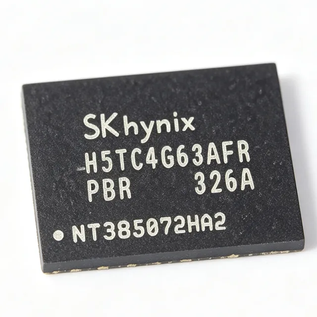
H5TC4G63AFR-PBR - 4Gb DDR3L SDRAM 256Mx16 | SK Hynix
MPN: H5TC4G63AFR-PBR ✓ Active| Qty | Unit Price | Extended |
|---|---|---|
| 1 | $8.5 | $8.50 |
| 10 | $7.8 | $78.00 |
| 100 | $7.1 | $710.00 |
| 500 | $6.5 | $3,250.00 |
| 1,000 | $5.9091 | $5,909.10 |
H5TC4G63AFR-PBR Overview
DDR3L SDRAM is a type of synchronous dynamic random-access memory that transfers data on both edges of the clock signal, effectively doubling the data rate. It is a low-voltage variant of DDR3, operating at 1.35V instead of 1.5V, which reduces power consumption by approximately 15-20% compared to standard DDR3. DDR3L is part of the DDR SDRAM family, which includes DDR, DDR2, DDR3, and DDR4, and is widely used in computing, networking, and embedded systems. The low-voltage operation makes it ideal for power-sensitive applications such as laptops, servers, and industrial electronics.
Key features of the H5TC4G63AFR-PBR include a 16-bit I/O interface, 8 internal banks, and a burst length of 8 (BL8) with burst chop (BC4). It supports auto refresh and self refresh modes, with a refresh interval of 7.8us at 85C and 3.9us at 95C. The device has a programmable output driver impedance and on-die termination for improved signal integrity. It also features a temperature-compensated self-refresh (TCSR) and a partial array self-refresh (PASR) for power savings. The package is a 96-ball FBGA with a 0.8mm ball pitch, measuring 13.5mm x 9.0mm, and is RoHS compliant.
Technically, the H5TC4G63AFR-PBR uses a CMOS process and supports a clock frequency up to 800 MHz (DDR3L-1600). It has a tCK of 1.25ns and a tRCD of 13.125ns. The device includes a mode register set (MRS) for configuration and supports write leveling and read leveling for improved signal integrity. The I/O interface is SSTL-15 compatible, and the device supports a data strobe (DQS) differential pair. The memory is organized into 8 banks of 32M x 16, providing a total capacity of 4Gb. The device is designed for high-reliability applications and is available in a lead-free, halogen-free package.
Typical applications for the H5TC4G63AFR-PBR include embedded systems, networking equipment (routers, switches), industrial PCs, and consumer electronics such as set-top boxes and smart TVs. Its low-voltage operation and high density make it suitable for memory-intensive applications where power efficiency is critical. The device is also used in automotive infotainment systems and medical devices that require reliable, high-speed memory.
When designing with this device, ensure proper decoupling capacitors (0.1uF and 1uF) are placed near the VDD and VDDQ pins to minimize noise. The VREFCA and VREFDQ should be bypassed with 0.1uF capacitors. The device requires a stable 1.35V supply and a separate 1.35V VDDQ supply. For optimal signal integrity, route the DQ, DQS, and address lines with matched trace lengths and controlled impedance (typically 50 ohms single-ended, 100 ohms differential).
Drop-in alternatives for H5TC4G63AFR-PBR — same package, pin-to-pin compatible. Different-package parts requiring PCB rework are excluded.
Variants in this series
Same-series models that are drop-in compatible with H5TC4G63AFR-PBR (same form factor and footprint) — differing in Burst Length, Package, Data Rate, CAS Latency, Operating Temperature.
Quick Comparison Tool — Select alternative parts for side-by-side comparison:
H5TC4G63AFR-PBA
✓ In Stock
$3.9773 / Unit
View Datasheet →H5TC4G63AFR-PBI
✓ In Stock
$6.5 / Unit
View Datasheet →H5TC4G63MFR-PBA
✓ In Stock
$6.5 / Unit
View Datasheet →H5TC4G63CFR-PBA
✓ In Stock
$6.23 / Unit
View Datasheet →K4B4G1646E-BMK0
✓ In Stock
$6.5 / Unit
View Datasheet →MT41K256M16HA-125:E
✓ In Stock
$3.1 / Unit
View Datasheet →NT5CC256M16DP-DI
✓ In Stock
$6.5 / Unit
View Datasheet →H5TC4G63AFR-PBR Maximum Ratings & Electrical Characteristics
| Memory Type | DDR3L SDRAM |
| Organization | 256M x 16 |
| Total Capacity | 4Gb |
| Supply Voltage | 1.35V (1.5V compatible) |
| Data Rate | 1600 Mbps (PC3L-12800) |
| CAS Latency | 11 |
| tRCD/tRP | 11 |
| Clock Frequency | 800 MHz |
| tCK | 1.25 ns |
| tRCD | 13.125 ns |
| Burst Length | 8 (BL8) with burst chop (BC4) |
| Number of Banks | 8 |
| Refresh Interval | 7.8us at 85C, 3.9us at 95C |
| Package | 96-ball FBGA (PBGA96) |
| Package Dimensions | 13.5mm x 9.0mm |
| Ball Pitch | 0.8mm |
| I/O Interface | SSTL-15 |
| Operating Temperature | 0C to +95C |
| RoHS | Compliant |
| Lead-Free | Yes |
| Halogen Free | Yes |
H5TC4G63AFR-PBR Pin Configuration
| Pin A1 | VDD — Power supply for core logic |
| Pin A2 | VSS — Ground |
| Pin A3 | DQ0 — Data input/output 0 |
| Pin A4 | DQ1 — Data input/output 1 |
| Pin A5 | VDDQ — Power supply for I/O |
| Pin A6 | VSSQ — Ground for I/O |
| Pin A7 | DQ2 — Data input/output 2 |
| Pin A8 | DQ3 — Data input/output 3 |
| Pin A9 | VDD — Power supply |
| Pin A10 | VSS — Ground |
| Pin B1 | VSS — Ground |
| Pin B2 | DQ4 — Data input/output 4 |
| Pin B3 | DQ5 — Data input/output 5 |
| Pin B4 | VDDQ — Power supply for I/O |
| Pin B5 | VSSQ — Ground for I/O |
| Pin B6 | DQ6 — Data input/output 6 |
| Pin B7 | DQ7 — Data input/output 7 |
| Pin B8 | VDD — Power supply |
| Pin B9 | VSS — Ground |
| Pin B10 | DQS0 — Data strobe 0 |
Typical Applications
H5TC4G63AFR-PBR is suitable for 6 applications: Embedded Systems, Networking Equipment, Industrial PCs, Consumer Electronics, Automotive Infotainment, Medical Devices.
Embedded Systems
The H5TC4G63AFR-PBR is ideal for embedded systems requiring high-density, low-power memory. Its 4Gb capacity and 1.35V operation reduce power consumption by up to 20% compared to standard DDR3, making it suitable for battery-powered devices. The 256M x 16 organization simplifies board layout with fewer chips, and the 1600 Mbps data rate supports demanding real-time processing. The 96-ball FBGA package with 0.8mm pitch enables compact designs, while the JEDEC DDR3L compliance ensures compatibility with a wide range of embedded controllers.
Recommended
Networking Equipment
In networking equipment such as routers and switches, the H5TC4G63AFR-PBR provides high-bandwidth packet buffering and routing table storage. Its 1600 Mbps data rate and 8 internal banks enable efficient burst transfers, while the low 1.35V supply reduces thermal load in dense chassis. The on-die termination and programmable output driver impedance improve signal integrity on high-speed traces, critical for reliable operation in noisy environments. The device's support for write leveling and read leveling simplifies PCB design for multi-rank configurations.
Recommended
Industrial PCs
The H5TC4G63AFR-PBR is well-suited for industrial PCs that require reliable operation over extended temperature ranges. With an operating temperature of 0C to +95C, it meets the demands of factory automation and process control. The 4Gb capacity supports multitasking and data logging, while the 1.35V operation reduces power consumption in always-on systems. The device's temperature-compensated self-refresh (TCSR) and partial array self-refresh (PASR) features further enhance power efficiency, making it ideal for fanless industrial designs.
Recommended
Consumer Electronics
In consumer electronics like set-top boxes and smart TVs, the H5TC4G63AFR-PBR delivers high-speed memory for smooth video playback and responsive user interfaces. Its 1600 Mbps data rate ensures sufficient bandwidth for HD video streams, while the low 1.35V supply helps meet energy efficiency standards. The 96-ball FBGA package allows for slim device designs, and the device's support for burst length 8 with burst chop optimizes memory access patterns for multimedia workloads. The JEDEC DDR3L compliance ensures interoperability with mainstream SoCs.
Recommended
Automotive Infotainment
The H5TC4G63AFR-PBR is used in automotive infotainment systems for navigation, media playback, and connectivity. Its 4Gb capacity supports complex user interfaces and map data, while the 1.35V operation reduces power draw from the vehicle's electrical system. The device's wide operating temperature range (0C to +95C) covers typical cabin environments, and its robust signal integrity features ensure reliable operation in electrically noisy automotive environments. The JEDEC DDR3L compliance guarantees compatibility with automotive-grade SoCs.
Recommended
Medical Devices
In medical devices such as patient monitors and diagnostic equipment, the H5TC4G63AFR-PBR provides reliable high-speed memory for data acquisition and processing. Its 4Gb capacity supports large data buffers for imaging and waveform analysis, while the low 1.35V supply reduces heat generation in compact enclosures. The device's high reliability and long lifecycle make it suitable for medical applications where downtime is unacceptable. The 96-ball FBGA package with 0.8mm pitch enables dense PCB layouts, and the JEDEC DDR3L compliance ensures compatibility with medical-grade processors.
Recommended
Recommended Products Summary
Engineering reference data for H5TC4G63AFR-PBR — comparison, design guidance, and compliance information.
Selection Guide
Comparison with Alternatives
| Parameter | This Product | H5TC4G63AFR-PBA | H5TC4G63AFR-PBI | H5TC4G63MFR-PBA | K4B4G1646E-BMK0 | MT41K256M16HA-125 | NT5CC256M16DP-DI |
|---|---|---|---|---|---|---|---|
| Package | 96-ball FBGA (PBGA96) | 96-ball FBGA (PBGA96) | 96-ball FBGA (PBGA96) | 96-ball FBGA (PBGA96) | 96-ball FBGA (PBGA96) | E: 96-ball FBGA (PBGA96) | 96-ball FBGA (PBGA96) |
| Brand | SK Hynix | SK Hynix | SK Hynix | SK Hynix | Samsung | E: Micron | Nanya |
| Memory Type | DDR3L SDRAM | DDR3L SDRAM | DDR3L SDRAM | DDR3L SDRAM | DDR3L SDRAM | E: DDR3L SDRAM | DDR3L SDRAM |
| Organization | 256M x 16 | 256M x 16 | 256M x 16 | 256M x 16 | 256M x 16 | E: 256M x 16 | 256M x 16 |
| Data Rate | 1600 Mbps | 1600 Mbps | 1600 Mbps | 1600 Mbps | 1600 Mbps | E: 1600 Mbps | 1600 Mbps |
| Supply Voltage | 1.35V | 1.35V | 1.35V | 1.35V | 1.35V | E: 1.35V | 1.35V |
| CAS Latency | 11 | 11 | 11 | 11 | 11 | E: 11 | 11 |
| Operating Temperature | 0C to +95C | 0C to +95C | -40C to +95C | 0C to +95C | 0C to +95C | E: 0C to +95C | 0C to +95C |
Key Differentiators
- Low-voltage operation (1.35V) reduces power consumption by 15-20% compared to standard DDR3 (vs K4B4G1646E-BMK0)
- Wide operating temperature range (0C to +95C) supports industrial applications (vs H5TC4G63AFR-PBI)
- JEDEC DDR3L compliance ensures broad compatibility (vs MT41K256M16HA-125:E)
Design Notes
The H5TC4G63AFR-PBR requires a stable 1.35V VDD and VDDQ supply. Use low-ESR ceramic capacitors (0.1uF and 1uF) placed close to each VDD and VDDQ pin to minimize noise. A bulk capacitor (10uF) on the board is recommended. Ensure the power supply can handle peak current during refresh and burst operations.
Route DQ, DQS, and address lines with matched trace lengths to maintain signal integrity. Use controlled impedance of 50 ohms single-ended and 100 ohms differential for DQS. Keep trace lengths within 100 mils of each other to minimize skew. Place VREFCA and VREFDQ bypass capacitors (0.1uF) close to the pins.
The H5TC4G63AFR-PBR dissipates minimal power due to 1.35V operation, but in high-density systems, ensure adequate airflow or thermal vias under the FBGA package. The maximum operating temperature is 95C; keep the junction temperature below this limit by providing proper heat spreading on the PCB.
Compliance Information
RoHS compliant per internal database. Lead-free and halogen-free package. AEC-Q100 not specified for this part.




