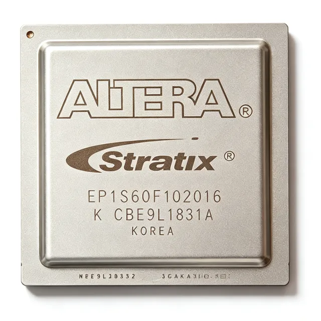
EP1S60F1020C5N - Stratix 57K LE, 1020-pin FBGA FPGA | Intel (Altera)
MPN: EP1S60F1020C5N ✗ End of Life| Qty | Unit Price | Extended |
|---|---|---|
| 1 | $2850 | $2,850.00 |
| 10 | $2680 | $26,800.00 |
| 100 | $2450 | $245,000.00 |
| 500 | $2240 | $1,120,000.00 |
| 1,000 | $2050 | $2,050,000.00 |
EP1S60F1020C5N Overview
An FPGA (Field-Programmable Gate Array) is a semiconductor integrated circuit whose logic function is defined by a customer-supplied configuration bitstream rather than at the wafer fab. The device family hierarchy is: FPGA -> programmable logic device (PLD) -> logic IC -> integrated circuit. Within Altera/Intel's portfolio, the Stratix family sits above Cyclone (cost-optimized) and below Stratix GX/GX-S/GT/II/III/V (transceiver-rich and high-end variants). The EP1S60 specifically occupies the high-density mid-range of the first-generation Stratix line, before the Stratix II architectural shift.
Key differentiating features include TriMatrix embedded memory blocks (three sizes: 512-bit M512, 4-Kbit M4K, 512-Kbit MRAM), embedded DSP blocks implementing 9-bit signed multipliers with accumulator chains, up to 12 high-speed transceiver channels (depending on speed grade), and a richly featured clock network with up to 16 dedicated clock pins and 16 PLL blocks. The 'N' suffix denotes lead-free / Pb-free termination.
The 'C5' speed grade places this part in the mid-speed bin of the Stratix family (C6 = fast commercial, C7 = faster commercial, C8 = fastest; C5 is commercial, 0 to 85 C junction). The 1020-pin FBGA package exposes nearly all of the device's I/O, enabling high pin-count designs including communications backplanes, ASIC prototyping, and high-density DSP systems. Each Stratix LE contains a 4-input LUT, a programmable register, carry-chain logic, and a register chain interconnect.
Typical applications include high-speed DSP (FFT, FEC, video processing), ASIC prototyping and emulation, telecom line-card glue logic, military/aerospace signal processing, and high-throughput data-path controllers. The abundant TriMatrix memory and DSP blocks make the EP1S60 especially attractive for SDR baseband, multi-channel video pipelines, and protocol bridging designs. Designs typically target the Quartus II design suite (version 5.x or later supporting Stratix) and use configuration via EPC16/EPC8 configuration devices or JTAG.
Designers should budget careful attention to power: a 57K-LE Stratix with high utilization can exceed 5 W to 15 W core power, requiring 1.5 V bulk decoupling of at least 330 uF low-ESR polymer plus per-pin bypass. The 'C5' speed grade is the slower of the commercial speed grades, favored over C6/C7/C8 when timing margin matters more than throughput. When designing, ensure the Quartus II fitter is set for the 1020-pin FBGA package and that pin-out assignments respect the bank's VCCIO groupings.
This page synthesizes the Stratix family datasheet specifications, current distributor pricing tiers, same-brand drop-in speed-grade and package variants, and practical design notes that complement the manufacturer datasheet. Pricing for the EP1S60F1020C5N is referenced as of 2026-09-07.
Drop-in alternatives for EP1S60F1020C5N — same package, pin-to-pin compatible. Different-package parts requiring PCB rework are excluded.
Variants in this series
Same-series models that are drop-in compatible with EP1S60F1020C5N (same form factor and footprint) — differing in Package, Speed Grade, Operating Temperature, Family, RoHS Status.
Quick Comparison Tool — Select alternative parts for side-by-side comparison:
EP1S60F1020C5
✓ In Stock
$171 / Unit
View Datasheet →EP1S60F1020C6N
✓ In Stock
$195 / Unit
View Datasheet →EP1S60F1020C7N
✓ In Stock
$1580 / Unit
View Datasheet →EP1S60F1020I6N
✓ In Stock
$3650 / Unit
View Datasheet →EP1S60F1020C8N
📋 Reference alternative (not in catalog)
EP1S60F1020I7N
📋 Reference alternative (not in catalog)
EP1S60F1020C5N Maximum Ratings & Electrical Characteristics
| Family | Stratix |
| Logic Elements (LEs) | 57,120 |
| Logic Array Blocks (LABs) | 6,570 |
| Total RAM Bits | 5,215,104 |
| Process Technology | 130 nm CMOS |
| Core Supply Voltage | 1.425 V to 1.575 V |
| Operating Temperature | 0 C to 85 C (commercial) |
| Speed Grade | C5 (commercial, slowest) |
| Package | 1020-ball FBGA (33 x 33 mm, 1 mm pitch) |
| Lead-Free (N suffix) | Yes |
| Mounting Type | Surface Mount |
| Logic Family | CMOS |
| Supplier Device Package | 1020-FBGA (33x33) |
EP1S60F1020C5N 1020-fbga (33x33) Pin Configuration Guide
Pin configuration for EP1S60F1020C5N (1020-fbga (33x33) package). This digital IC includes GPIO, communication interfaces (UART, SPI, I2C), and power pins. Refer to the manufacturer datasheet for alternate pin functions and configuration options. Essential for embedded system design and PCB layout.

No detailed pinout data available for EP1S60F1020C5N.
Refer to the datasheet for full pin configuration.
Typical Applications
EP1S60F1020C5N is suitable for 7 applications: High-Speed DSP (FFT / FEC / Video Codecs), ASIC Prototyping and Emulation, Telecom Line-Card Glue Logic and Protocol Bridging, Military / Aerospace Signal Processing, Multi-Channel Video Pipeline Processing, Software-Defined Radio Baseband, High-Density Data-Path Controller / Storage Bridge.
High-Speed DSP (FFT / FEC / Video Codecs)
The EP1S60F1020C5N fits high-speed DSP applications because its 57,120 logic elements plus dedicated embedded DSP blocks (9-bit signed multipliers with accumulator chains) deliver hundreds of GMACs of throughput at the C5 speed grade. The 5,215,104 bits of TriMatrix memory (M512, M4K, MRAM) sit adjacent to DSP blocks to minimize routing delay, enabling pipelined radix-2^2 FFTs up to several hundred MSPS. The 1020-pin FBGA exposes enough user I/O to feed parallel data streams without bottlenecking the compute fabric. Quartus II auto-packs DSP inference patterns and reports Fmax in the timing analyzer. For new designs targeting higher DSP throughput per watt, the Stratix II EP2S60 is recommended.
Recommended
ASIC Prototyping and Emulation
The EP1S60F1020C5N is well-suited to ASIC prototyping because its 57,120 LEs, abundant DSP blocks, and 5 Mbit of embedded memory map ASIC RTL directly without forcing heavy partitioning. The 1020-ball FBGA exposes close to 800 user I/O, enabling connection to multiple ASIC die pads through a single FPGA footprint. Multiple EP1S60 devices can be co-emulated via SelectMap or JTAG chains to support larger ASIC gate counts. Quartus II supports incremental compilation so multiple designers can compile independent partitions into one bitstream. Note that the C5 speed grade is the slowest commercial grade; timing-critical ASIC blocks may need a faster alternative like EP1S60F1020C7N. Configuration via EPC16 or JTAG is straightforward.
Recommended
Telecom Line-Card Glue Logic and Protocol Bridging
The EP1S60F1020C5N fits telecom line-card designs because it integrates rich logic, 5 Mbit of TriMatrix memory, and DSP blocks with sufficient I/O to bridge protocols such as SPI, I2C, UART, POS-PHY, Utopia, and Serial RapidIO. The 1020-ball FBGA supplies enough LVDS pairs for telecom backplane interfaces, while 16 dedicated clock pins and up to 16 PLLs handle multiple telecom-grade reference clocks with jitter well below 100 ps. Industrial-temp variants (EP1S60F1020I6N) extend operation to -40 to +100 C for outdoor and central-office environments. Quartus II includes IP cores for most telecom standards; the C5 speed grade meets typical 100-200 MHz line-card glue-logic rates.
Recommended
Military / Aerospace Signal Processing
The EP1S60F1020C5N (or its industrial/extended variants) is used in military and aerospace signal-processing applications because the high LE count, abundant embedded memory, and DSP blocks support radar, EW, and SIGINT data paths. The 1020-ball FBGA withstands vibration typical of airborne platforms, and Altera's military-grade flow includes lot acceptance testing. Industrial temp variants extend the operating envelope beyond 0 to 85 C; for full MIL-PRF screening consider the EP1S60F1020I8N variant if qualified. The C5 speed grade is conservative for timing closure in safety-critical designs. Designers should budget for SEL/SEU mitigation via TMR or scrubbing with a watchdog configuration device.
Recommended
Multi-Channel Video Pipeline Processing
The EP1S60F1020C5N supports multi-channel video pipelines because its 57,120 LEs and embedded DSP blocks can drive H.264, MPEG-2, JPEG2000 codecs, and color-space converters at SD/HD rates with headroom for 3D video processing. The 5 Mbit of TriMatrix memory acts as line/frame buffers between pipeline stages without forcing external DDR. The 1020-ball FBGA provides enough parallel LVDS pairs to drive CameraLink, DVI, or HDMI outputs directly. Quartus II includes Video and Image Processing (VIP) IP cores and reference designs that target this exact device family. Industrial-temp variants allow outdoor broadcast equipment. New designs should evaluate Stratix II EP2S60 for higher DSP throughput at lower power.
Recommended
Software-Defined Radio Baseband
The EP1S60F1020C5N fits SDR baseband designs because its 57,120 LEs plus dedicated DSP blocks support multi-channel DDC/DUC, FFTs, and channelization filters at LTE, WiMAX, and legacy 3G sample rates. The 5 Mbit of TriMatrix memory holds coefficients and reordering buffers, while 1020 user I/O pins accept parallel ADC/DAC data streams. The device supports up to 12 high-speed transceiver channels (speed-grade dependent), enabling CPRI or OBSAI links to remote radio heads. Quartus II provides DSP Builder for model-based design entry from MATLAB/Simulink. For new designs targeting carrier-grade LTE-A throughput, evaluate the Stratix IV GT or Stratix V GX, which integrate multi-Gbps transceivers natively.
Recommended
High-Density Data-Path Controller / Storage Bridge
The EP1S60F1020C5N serves as a high-density data-path controller or storage bridge because its abundant LE count and 5 Mbit TriMatrix memory support complex DMA engines, RAID controllers, and protocol adapters (SATA, SAS, Fibre Channel, PCIe) at line rates up to several Gbps. The 1020-ball FBGA exposes enough LVDS pairs for multi-lane PCIe Gen1, SATA-II, or SAS interfaces when paired with external PHYs. Embedded DSP blocks accelerate XOR and Reed-Solomon computations for RAID-6 and erasure coding. Industrial-temp variants suit enterprise storage appliances. New designs targeting 10+ Gbps line rates should consider Stratix V GX or Stratix 10 with native hard PCIe Gen3 controllers.
Recommended
Recommended Products Summary
Engineering reference data for EP1S60F1020C5N — comparison, design guidance, and compliance information.
Selection Guide
Comparison with Alternatives
| Parameter | This Product | EP1S60F1020C5 | EP1S60F1020C6N | EP1S60F1020C7N | EP1S60F1020C8N | EP1S60F1020I6N | EP1S60F1020I7N |
|---|---|---|---|---|---|---|---|
| Package | 1020-ball FBGA (33x33 mm) | 1020-ball FBGA (33x33 mm) | 1020-ball FBGA (33x33 mm) | 1020-ball FBGA (33x33 mm) | 1020-ball FBGA (33x33 mm) | 1020-ball FBGA (33x33 mm) | 1020-ball FBGA (33x33 mm) |
| Brand | Intel (Altera) | Intel (Altera) | Intel (Altera) | Intel (Altera) | Intel (Altera) | Intel (Altera) | Intel (Altera) |
| Speed Grade | C5 (slowest commercial) | C5 | C6 (faster) | C7 (faster) | C8 (fastest) | I6 (industrial) | I7 (industrial, faster) |
| Operating Temperature | 0 to +85 C (commercial) | 0 to +85 C | 0 to +85 C | 0 to +85 C | 0 to +85 C | -40 to +100 C | -40 to +100 C |
| Logic Elements | 57,120 LEs | 57,120 LEs | 57,120 LEs | 57,120 LEs | 57,120 LEs | 57,120 LEs | 57,120 LEs |
| Total RAM Bits | 5,215,104 bits | 5,215,104 bits | 5,215,104 bits | 5,215,104 bits | 5,215,104 bits | 5,215,104 bits | 5,215,104 bits |
| Logic Array Blocks | 6,570 LABs | 6,570 LABs | 6,570 LABs | 6,570 LABs | 6,570 LABs | 6,570 LABs | 6,570 LABs |
| Lead-Free (N suffix) | Yes (Pb-free) | No (SnPb) | Yes (Pb-free) | Yes (Pb-free) | Yes (Pb-free) | Yes (Pb-free) | Yes (Pb-free) |
| Core Voltage | 1.425 to 1.575 V | 1.425 to 1.575 V | 1.425 to 1.575 V | 1.425 to 1.575 V | 1.425 to 1.575 V | 1.425 to 1.575 V | 1.425 to 1.575 V |
| Process Technology | 130 nm CMOS | 130 nm CMOS | 130 nm CMOS | 130 nm CMOS | 130 nm CMOS | 130 nm CMOS | 130 nm CMOS |
Key Differentiators
- Slowest commercial speed grade maximizes timing margin (vs EP1S60F1020C7N)
- Lead-free (N suffix) ball finish for RoHS compliance (vs EP1S60F1020C5)
- Highest-pin-count Stratix variant exposes maximum user I/O (vs EP1S60F780C5N (780-pin variant))
Design Notes
Estimated: A fully-utilized 57,120-LE Stratix EP1S60 can dissipate 5 W to 15 W core power at 1.5 V depending on toggle rate. Provide at least 330 uF of bulk low-ESR polymer capacitance plus 100 uF of high-frequency ceramic on each VCC plane (VCCINT, VCCIO, VCCAUX). Use 1 oz copper on inner power planes and 2 oz on outer layers for the core island. Decouple each PLL VCCA pin with 0.1 uF plus 10 uF within 5 mm of the pin. Strap VCCIO banks per I/O standard: 3.3 V, 2.5 V, 1.8 V, or 1.5 V.
Estimated: The 33 x 33 mm 1020-ball FBGA package's theta_JA is approximately 11 C/W with 1 m/s airflow, giving a 110 C rise for 10 W dissipation. A heatsink plus thermal pad is strongly recommended above 8 W continuous. For full industrial-temperature operation (-40 to +100 C junction), use EP1S60F1020I6N or I7N. Mounting the FBGA requires BGA-grade PCB (ENIG or ENEPIG surface finish) with microvia stack-ups to fan out the 1 mm ball pitch; avoid HASL finishes.
Route all 1020 balls of the EP1S60F1020C5N through a microvia-in-pad PCB stack-up: 1+6+1 (signal-ground-signal-power-signal-ground-signal-power-signal) or similar. Match differential pair lengths within 5 mil for LVDS data rates above 500 Mbps. Place the EPC16 configuration device on the same board layer as the FPGA to minimize trace length below 6 inches. Provide a JTAG header (TCK, TMS, TDI, TDO, TRST, VCCIO_REF, GND) per IEEE 1149.1 for boundary-scan and in-system programming.
The EP1S60F1020C5N has 16 dedicated clock pins (CLK[15..0]) and up to 16 PLLs; route each clock trace as a 50 ohm microstrip with matched length within 50 mil of other clocks in the same PLL domain. Keep high-speed transceiver (if present at C5 speed grade) traces length-matched within 12 mil for the entire channel. Use ground vias every 200 mil along LVDS pairs to maintain impedance and return-path integrity. Avoid routing signals over split power planes; keep VCCINT return paths clear.
Critical pitfalls: (1) The C5 speed grade is the slowest commercial grade - do not assume it meets timing at 300+ MHz internal Fmax; check the Quartus II timing analyzer carefully. (2) Do not mix 5 V-tolerant I/O with 3.3 V on the same bank; VCCIO must match bank-wide. (3) Configuration via JTAG without proper VCCIO_REF connection fails silently. (4) The 'C5' (without N) variant uses SnPb balls - mixing with Pb-free assembly profiles causes joint defects. (5) Do not populate the FPGA without first programming a known-good bitstream via JTAG; an unconfigured EP1S60 leaves all I/O floating.
Compliance Information
EP1S60F1020C5N has lead-free (Pb-free) ball finish per the 'N' suffix, RoHS compliant per Intel/Altera product page. AEC-Q100 not applicable for FPGAs. Conflict-minerals compliance per Intel supplier declaration.







