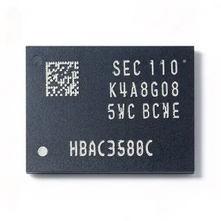
K4AAG085WA-BCPB - 16Gb DDR4 SDRAM 2Gx8 | Samsung
MPN: K4AAG085WA-BCPB ✓ Active| Qty | Unit Price | Extended |
|---|---|---|
| 1 | $8.51 | $8.51 |
| 10 | $8.08 | $80.80 |
| 100 | $7.66 | $766.00 |
| 500 | $7.28 | $3,640.00 |
| 1,000 | $6.92 | $6,920.00 |
K4AAG085WA-BCPB Overview
A DDR4 SDRAM (Double Data Rate 4 Synchronous Dynamic Random Access Memory) is a volatile memory IC that transfers data on both clock edges, doubling effective bandwidth versus DDR3 at the same clock. Within the memory hierarchy it sits at the DRAM level: memory IC -> DRAM -> DDR SDRAM -> DDR4 SDRAM -> system main memory. DDR4 lowers operating voltage from 1.5 V (DDR3) to 1.2 V and raises bank-group parallelism with bank group architecture for higher data rates.
Key features of the K4AAG085WA family include 16 Gbit density in a x8 organization, 1.2 V core supply, DDR4 bank group architecture, on-die termination (ODT), DLL-enabled mode operation, and the compact 78FBGA surface-mount package. Speed grades within the WA family reach up to 3200 Mbps pin speed (as documented for the BCWE grade). The BCPB suffix identifies a specific speed bin and commercial temperature range; engineers must confirm the exact bin timing parameters from the Samsung datasheet before design lock.
Architecturally, the device uses an 8-bank or bank-group structure with burst lengths of 8 (BL8), programmable CAS latency, and activation/power-down management per the DDR4 SDRAM standard protocol. The datasheet abstract notes that timings specified apply to DLL-enabled mode of operation.
Typical applications include server DIMMs and memory modules, desktop PC main memory, embedded industrial controllers requiring high-density DRAM, networking equipment buffering, and AI/edge compute platforms where 16 Gbit-per-chip density reduces component count.
Design consideration: DDR4 routing requires length-matched, impedance-controlled fly-by topology for command/address lines and ODT calibration during init; confirm speed-bin timings against your memory controller.
This page synthesizes verified distributor data, same-package drop-in alternatives, and engineering design notes not found in the manufacturer datasheet alone.
Drop-in alternatives for K4AAG085WA-BCPB — same package, pin-to-pin compatible. Different-package parts requiring PCB rework are excluded.
Variants in this series
Same-series models that are drop-in compatible with K4AAG085WA-BCPB (same form factor and footprint) — differing in Interface, Package, Density, Operating Temperature, RoHS Status.
Quick Comparison Tool — Select alternative parts for side-by-side comparison:
K4AAG085WA-BCWE
✅ Drop-In✓ In Stock
$7.24 / Unit
View Datasheet →K4AAG085WA-BCTD
✅ Drop-In ⚠️ Specs Unverified✓ In Stock
$10.18 / Unit
View Datasheet →K4AAG085WA-BIWE
✅ Drop-In📋 Reference alternative (not in catalog)
K4AAG085WB-BCPB
✅ Drop-In ⚠️ Specs Unverified📋 Reference alternative (not in catalog)
K4AAG085WA-BCPB Maximum Ratings & Electrical Characteristics
| Memory Type | DDR4 SDRAM |
| Density | 16 Gbit |
| Organization | 2G x 8 |
| Supply Voltage | 1.2 V |
| Package | 78FBGA |
| Mounting Type | Surface Mount |
| Operating Temperature | 0 C to 85 C (commercial grade, per K4AAG085WA family data) |
| Interface | Parallel (DDR4) |
| Clock Type | Synchronous, differential clock |
| Bank Architecture | DDR4 bank group architecture |
| DLL Mode | DLL Enabled mode operation (per Samsung datasheet abstract) |
| Memory Format | DRAM |
| RoHS Status | Compliant (per family listing on JLCPCB) |
| Temperature Grade Code | C (per Samsung part number coding) |
| Speed Bin Code | PB (per Samsung part number coding) |
K4AAG085WA-BCPB 78fbga Pin Configuration Guide
Pin configuration for K4AAG085WA-BCPB (78fbga package). This digital IC includes GPIO, communication interfaces (UART, SPI, I2C), and power pins. Refer to the manufacturer datasheet for alternate pin functions and configuration options. Essential for embedded system design and PCB layout.

No detailed pinout data available for K4AAG085WA-BCPB.
Refer to the datasheet for full pin configuration.
Typical Applications
K4AAG085WA-BCPB is suitable for 6 applications: Server Memory Modules (RDIMM/LRDIMM), Desktop PC Main Memory, Embedded Industrial Controllers, Networking and Telecom Equipment, AI Edge and Vision Processing, Test, Measurement and Compute Accelerators.
Server Memory Modules (RDIMM/LRDIMM)
Server DIMM designers choose the K4AAG085WA-BCPB because 16 Gbit per chip maximizes capacity per rank: a single-rank x8 ECC DIMM uses 72 of these chips (with 8 for ECC) to reach 16 GB per rank, halving chip count versus 8 Gbit parts and reducing load on the fly-by command/address bus. The 1.2 V rail cuts module dynamic power relative to DDR3 at comparable bandwidth, improving performance-per-watt in data centers. The chip operates in DLL-enabled mode with BL8 bursts across DDR4 bank groups, and its registered-module environment handles initialization, ODT calibration, and ZQ calibration via the module's register and PMIC. The trade-off is the commercial 0 to 85 C temperature code, so near-socket thermal budgets must keep Tcase within range.
Recommended
Desktop PC Main Memory
Consumer desktop platforms benefit from the K4AAG085WA-BCPB's density-per-chip advantage: two 16 Gbit x8 chips deliver 4 GB of a UDIMM rank, letting motherboard vendors build 8 GB single-rank DIMMs with only four ICs, which simplifies routing and lowers bill-of-material cost. The 2G x 8 organization pairs naturally with x64 memory controller channels in 8-chip ranks, and the 1.2 V supply matches standard DDR4 UDIMM power delivery. DDR4 bank group architecture sustains the sustained bandwidth desktop workloads expect, while ODT and DBI-style I/O tuning in the controller recover signal integrity on four-layer module PCBs. Designers should configure the memory controller to the BCPB speed bin's published CAS latency and timings and validate with the Samsung datasheet timing tables, not family-generic numbers.
Recommended
Embedded Industrial Controllers
Industrial gateways, machine-vision controllers, and edge IPCs use the K4AAG085WA-BCPB where a single 16 Gbit chip provides 2 GB of DRAM in a 78FBGA footprint of roughly 10 x 15 mm, saving board area versus multiple 8 Gbit devices. The 1.2 V core suits fanless enclosures by lowering self-heating, and DDR4's bank group architecture keeps burst latency predictable for real-time data logging and protocol processing. The commercial 0 to 85 C operating range covers most cabinet environments, but designers must verify junction temperature with local ambient derating; for unheated outdoor cabinets, the industrial-grade K4AAG085WA-BIWE variant in the same footprint is the safer pick. Initialization requires controller-driven MRS, ZQ calibration, and ODT programming per the DDR4 protocol, which modern SoC memory controllers handle automatically.
Recommended
Networking and Telecom Equipment
Switches, routers, and 5G baseband cards buffer packets and flow tables in DRAM, and the K4AAG085WA-BCPB fits this role with 16 Gbit density and 2G x 8 organization that maps cleanly onto 64-bit network processor memory controllers using eight chips per rank. DDR4's bank group architecture and BL8 bursts sustain the streaming read/write patterns of packet buffering, while the 1.2 V supply eases thermal design in 1U chassis with restricted airflow. Because telecom lines cards run continuously, derate the 85 C commercial limit against internal chassis temperature and verify the BCPB speed bin meets your controller's timing table. For redundant designs, the drop-in K4AAG085WA-BCWE provides a faster-bin second source within Samsung, simplifying supply-chain qualification across product refreshes.
Recommended
AI Edge and Vision Processing
Edge AI modules and smart-camera SoCs with DDR4 memory controllers use the K4AAG085WA-BCPB to host neural-network weight buffers and frame buffers: 2 GB from one 16 Gbit chip keeps layout compact around vision processors, and the x8 organization supports the 64-bit or 32-bit buses typical of edge SoCs with four or eight chips. The 1.2 V operation is critical for battery- or PoE-powered cameras where every watt counts, and the 78FBGA package reflows on standard SMT lines. Frame-buffer workloads favor the predictable bandwidth of DDR4 bank groups over shared LPDDR solutions in industrial cameras. Confirm the controller's DQ trace length matching supports the 78FBGA ball-out and program ODT values from the Samsung datasheet for your line impedance.
Recommended
Test, Measurement and Compute Accelerators
Instrumentation and accelerator cards capture and process large datasets, and the K4AAG085WA-BCPB provides 2 GB per chip for deep capture memory in oscilloscopes, logic analyzers, and FPGA-based accelerators. DDR4's higher data rates (family grades up to 3200 Mbps at the BCWE bin) give FPGA memory controllers the raw bandwidth for streaming ADC data to storage, while the 2G x 8 organization aligns with common 64-bit and 72-bit ECC datapaths. The commercial 0 to 85 C range covers benchtop instruments; rack-mounted systems should verify internal ambient against the limit. Because acquisition buffers are write-heavy, designers should enable DDR4 write CRC where the controller supports it and follow Samsung's DLL-enabled mode timing tables for the BCPB bin during controller calibration.
Recommended
Recommended Products Summary
Engineering reference data for K4AAG085WA-BCPB — comparison, design guidance, and compliance information.
Selection Guide
Comparison with Alternatives
| Parameter | This Product | K4AAG085WA-BCWE | K4AAG085WA-BCTD | K4AAG085WA-BIWE | K4AAG085WB-BCPB |
|---|---|---|---|---|---|
| Package | 78FBGA | 78FBGA - same | 78FBGA - same | 78FBGA - same | 78FBGA - same |
| Brand | Samsung Electronics | Samsung Electronics | Samsung Electronics | Samsung Electronics | Samsung Electronics |
| Density | 16 Gbit | 16 Gbit | 16 Gbit | 16 Gbit | 16 Gbit |
| Organization | 2G x 8 | 2G x 8 | 2G x 8 | 2G x 8 | 2G x 8 |
| Supply Voltage | 1.2 V | 1.2 V | 1.2 V | 1.2 V | 1.2 V |
Key Differentiators
- 16 Gbit density halves chip count versus 8 Gbit parts (vs K4A8G085WB-BCPB)
- Faster-bin drop-in available within the same package (vs K4AAG085WA-BCWE)
- Industrial temperature option on the same footprint (vs K4AAG085WA-BIWE)
Design Notes
DDR4 x8 interfaces at multi-gigabit rates require length-matched fly-by routing for command/address and point-to-point matched DQ/DQS per byte lane. Keep DQ-to-DQS skew within controller spec, reference signals to solid power/ground planes, and set on-die termination (ODT) values per the Samsung datasheet for your trace impedance (typically 40/50 ohm). Run the memory controller's write-leveling and read-training at bring-up; DDR4 does not tolerate legacy DDR3 static timing assumptions.
The device runs from a 1.2 V DDR4 rail; provide dedicated bulk and high-frequency decoupling (multiple 100 nF ceramics per device plus bulk capacitance per rail) with low-inductance via fan-out to the 78FBGA power balls. Estimated: at ~1.2 V and typical DRAM active currents of several hundred milliamps per device, supply ripple should be held to the DDR4 tolerance band; confirm exact IDD figures from the Samsung datasheet IDD tables for the BCPB bin rather than family-generic values.
The C temperature code denotes a 0 to 85 C commercial operating range. Estimated: FBGA DRAM junction temperature tracks case temperature closely; in enclosed server or telecom chassis, measure Tcase near the package top under full bandwidth workloads and add airflow or spreader copper if within 10 C of the 85 C limit. For uncontrolled ambient environments, select the industrial-grade K4AAG085WA-BIWE in the identical footprint instead.
Do not mix speed bins casually across a rank: although BCPB and BCWE share the 78FBGA footprint and protocol, the controller must be programmed with the slowest bin's timings. Also note the datasheet abstract states timings apply to DLL-enabled mode only - designs operating DLL-off (self-refresh-dominant, low-power modes) must consult the separate DLL-disabled timing tables. Samsung reserves the right to change specifications without notice; re-verify the latest datasheet revision before each production build.
Compliance Information
RoHS stated for family part K4AAG085WA-BCWE on JLCPCB listing ('FBGA-78 DRAM ROHS'); same-family inference for BCPB. REACH/halogen-free/conflict-minerals declarations not present in verified data - request from Samsung.