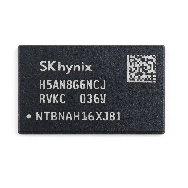
H5AN8G6NCJR-RDC - 8Gb DDR4 SDRAM 512Mx16 TFBGA-96 | SK hynix
MPN: H5AN8G6NCJR-RDC ✓ Active| Qty | Unit Price | Extended |
|---|---|---|
| 1 | $33.75 | $33.75 |
| 10 | $24.375 | $243.75 |
| 100 | $21.5625 | $2,156.25 |
| 500 | $20.625 | $10,312.50 |
| 1,000 | $19.6875 | $19,687.50 |
H5AN8G6NCJR-RDC Overview
DDR4 SDRAM is a type of dynamic random-access memory that replaced DDR3 in the DRAM hierarchy. As a member of the broader semiconductor memory family (DRAM -> synchronous DRAM -> DDR SDRAM -> DDR4 SDRAM), it transfers data on both clock edges, uses a lower operating voltage than DDR3, and integrates bank-group architectures to boost effective bandwidth in embedded and compute systems.
Key features of the H5AN8G6NCJR family include auto self-refresh, auto precharge, asynchronous reset, data mask (DM), write leveling, CRC, dynamic on-chip termination (ODT), and ZQ calibration, per SK hynix product data. The 512Mx16 organization allows a single 8Gb device to populate a 16-bit-wide memory bus, reducing component count in cost-sensitive designs.
Architecturally, the device offers fully synchronous operation referenced to both edges of the differential clock, internal bank-group parallelism, and programmable termination for signal integrity at DDR4 data rates. The CMOS process supports industrial-grade main memory subsystems with high bandwidth density per square centimeter of PCB area.
Typical applications include embedded main memory for industrial controllers, networking equipment line cards, set-top boxes, and memory modules or soldered-down memory in x86/ARM compute platforms where a x16 DDR4 device is required.
When designing this part in, observe DDR4 fly-by termination topology, route address/command with matched lengths, and verify ZQ calibration resistor placement per JEDEC DDR4 layout practice for best signal integrity.
This page synthesizes distributor pricing, drop-in same-package alternatives, practical design notes, and comparison data not found in the SK hynix datasheet, giving engineers a single decision-ready reference for the H5AN8G6NCJR-RDC.
Drop-in alternatives for H5AN8G6NCJR-RDC — same package, pin-to-pin compatible. Different-package parts requiring PCB rework are excluded.
Variants in this series
Same-series models that are drop-in compatible with H5AN8G6NCJR-RDC (same form factor and footprint) — differing in Package, RoHS Status, Mounting Type, Organization, Density.
Quick Comparison Tool — Select alternative parts for side-by-side comparison:
H5AN8G6NAFR-RDC
✓ In Stock
$3.05 / Unit
View Datasheet →H5AN8G6NCJR-VKC
✓ In Stock
$60 / Unit
View Datasheet →H5AN8G6NAFR-PBC
✓ In Stock
$3.55 / Unit
View Datasheet →H5AN8G8NCJR-RDC
✓ In Stock
$2.7 / Unit
View Datasheet →H5AN8G8NCJR-PBC
✓ In Stock
$2.4 / Unit
View Datasheet →H5AN8G6NCJR-XNC
📋 Reference alternative (not in catalog)
H5AN8G6NCJR-RDC Maximum Ratings & Electrical Characteristics
| Memory Density | 8 Gb (8589934592 bit) |
| Organization | 512M x 16 |
| Memory Type | DDR4 SDRAM |
| Technology | CMOS |
| Package Code | TFBGA (PBGA96) |
| Package Shape | Rectangular |
| Number of Terminals | 96 |
| Mounting Type | Surface Mount |
| Temperature Grade | OTHER |
| Auto Self-Refresh | Yes |
| Auto Precharge | Yes |
| Asynchronous Reset | Yes |
| Data Mask Function | Yes |
| Write Leveling | Yes |
| CRC | Yes |
| Dynamic On-Chip Termination | Yes |
| ZQ Calibration | Yes |
| RoHS Status | Lead-Free & Halogen-Free (RoHS Compliant, per H5AN8G6 family datasheet) |
H5AN8G6NCJR-RDC rectangular Pin Configuration Guide
Pin configuration for H5AN8G6NCJR-RDC (rectangular package). This digital IC includes GPIO, communication interfaces (UART, SPI, I2C), and power pins. Refer to the manufacturer datasheet for alternate pin functions and configuration options. Essential for embedded system design and PCB layout.

No detailed pinout data available for H5AN8G6NCJR-RDC.
Refer to the datasheet for full pin configuration.
Typical Applications
H5AN8G6NCJR-RDC is suitable for 6 applications: Embedded Main Memory for Industrial Controllers, Networking Equipment Line Cards, Set-Top Box and Smart Home Media Hubs, Soldered-Down Memory for x86/ARM Compute Modules, Test and Measurement Instrument Buffers, Automotive-Adjacent Infotainment and Telematics.
Embedded Main Memory for Industrial Controllers
Industrial PLCs and edge controllers need dense, high-bandwidth working memory in a small footprint. The H5AN8G6NCJR-RDC provides 8Gb of DDR4 in a single 512Mx16 device, letting a controller populate a 16-bit DDR4 bus with one package instead of two x8 parts, cutting component count and BOM cost. Features such as auto self-refresh preserve memory contents during low-power states, while ZQ calibration and dynamic on-chip termination maintain signal integrity across -40C to +85C-class industrial thermal profiles. Placed in fly-by topology with matched-length address/command routing, the device sustains DDR4 data rates with margin; thermal budgeting should confirm junction temperature at sustained access duty cycles.
Recommended
Networking Equipment Line Cards
Switch and router line cards buffer packet data in large DDR4 working memory with high sustained bandwidth. The H5AN8G6NCJR-RDC's 8Gb density in a 96-ball TFBGA supports high memory capacity per square centimeter of board area, and its CRC and write-leveling support align with the signal-integrity requirements of multi-rank DDR4 layouts in telecom hardware. The 512Mx16 organization allows designers to build 32-bit or 64-bit buses with two or four devices, balancing depth and bandwidth. Because line cards run 24/7, verifying the -RDC speed bin's refresh and derating tables against worst-case ambient (typically 45C-55C inlet) is essential for retention margin.
Recommended
Set-Top Box and Smart Home Media Hubs
Consumer media platforms require 1-2 GB of soldered-down DDR4 for video decode buffers and application memory. The H5AN8G6NCJR-RDC offers 8Gb (1 GB) per package in 512Mx16 organization, so a single device or a pair covers typical STB memory maps while keeping PCB area minimal. Auto self-refresh reduces standby power in always-on smart-home devices, and the asynchronous reset function simplifies power-rail sequencing design with the SoC. Its consumer-grade bin keeps unit cost low versus industrial bins; the trade-off is a narrower qualified temperature range, so enclosure thermal design should keep junction temperature within the datasheet limit during sustained 4K video playback.
Recommended
Soldered-Down Memory for x86/ARM Compute Modules
Compute-on-module and single-board computer designers increasingly solder DDR4 directly to the board to eliminate connector cost and improve reliability in vibration-prone environments. The H5AN8G6NCJR-RDC's 96-ball TFBGA footprint suits soldered-down implementations, and the 512Mx16 organization pairs naturally with 16-bit and 32-bit memory controllers in ARM SoCs. Using DDR4 features such as dynamic on-chip termination and ZQ calibration, the device maintains timing margin on short, densely routed point-to-point traces. Firmware should be configured with the -RDC bin's CAS latency and timing tables; designers should reserve board pull-up flexibility for ZQ and reset balls per the SK hynix datasheet reference design.
Recommended
Test and Measurement Instrument Buffers
Oscilloscopes, logic analyzers, and signal generators require deep acquisition memory with deterministic latency. The H5AN8G6NCJR-RDC supplies 8Gb per device in a compact TFBGA-96 package, allowing instrument front-ends to assemble gigabit-class buffer pools from a few components. The CRC and write-leveling features support the aggressive multi-drop topologies typical of instrument mainboards, while ZQ calibration keeps output impedance tracking process and temperature drift. Acquisition pipelines benefit from the fully synchronous double-data-rate operation referenced to both clock edges, giving predictable read turnaround. For long-record-depth modes, designers should model refresh-interval impact on sustained write bandwidth using the -RDC bin's tREFI parameters from the SK hynix datasheet.
Recommended
Automotive-Adjacent Infotainment and Telematics
Non-safety infotainment, navigation, and telematics control units in vehicles use soldered-down DDR4 for map and media buffering. The H5AN8G6NCJR-RDC's 8Gb density supports full-region map databases and cockpit graphics frame buffers in one package per 16-bit controller channel, reducing board complexity in space-constrained head units. Auto precharge and auto self-refresh streamline driver firmware and cut idle power in always-listening voice systems. For vehicles, the standard -RDC temperature class must be validated against the in-dash thermal profile (often up to +85C ambient near the display); if the platform requires AEC-qualified memory, an automotive-grade DDR4 should be selected instead of this consumer-class bin.
Recommended
Recommended Products Summary
Engineering reference data for H5AN8G6NCJR-RDC — comparison, design guidance, and compliance information.
Selection Guide
Comparison with Alternatives
| Parameter | This Product | H5AN8G6NAFR-RDC | H5AN8G6NCJR-VKC | H5AN8G6NCJR-XNC | H5AN8G8NCJR-RDC |
|---|---|---|---|---|---|
| Package | TFBGA-96 (PBGA96) | TFBGA-96 - same | TFBGA-96 - same | TFBGA-96 - same | TFBGA-96 - same |
| Brand | SK hynix | SK hynix | SK hynix | SK hynix | SK hynix |
| Memory Density | 8 Gb | 8 Gb | 8 Gb | 8 Gb | 8 Gb |
| Organization | 512M x 16 | 512M x 16 | 512M x 16 | 512M x 16 | 1G x 8 |
| Speed Bin | RDC | RDC (same) | VKC (2666 Mbps-class) | XNC | RDC (same) |
| Data Mask / Write Leveling / CRC | Yes / Yes / Yes | Yes / Yes / Yes | Yes / Yes / Yes | Yes / Yes / Yes | Yes / Yes / Yes |
Key Differentiators
- Same -RDC speed bin with current die revision (vs H5AN8G6NCJR-VKC)
- Broader temperature tolerance than standard bin (vs H5AN8G6NCJR-XNC)
- x16 bus width halves device count on 16-bit buses (vs H5AN8G8NCJR-RDC)
Design Notes
Route DDR4 in fly-by topology for address/command with on-die termination (ODT) enabled, and use point-to-point routing for DQ/DM/DQS per SK hynix datasheet layout guidance. Keep DQ/DQS length matching within controller specification (typically a few mils intra-byte). Enable write leveling during controller training to close timing at the -RDC bin's data rate, and verify ZQ calibration resistor (RZQ, typically 240 ohm 1%) placement close to the ZQ ball with a low-inductance ground return.
DDR4 uses separate VDD, VDDQ rails with the asynchronous reset (RESET_n) requiring correct sequencing relative to power rails per the SK hynix datasheet power-up sequence. Estimated: at DDR4-class I/O activity on a x16 bus, VDDQ current can reach hundreds of milliamps per device - size the PMIC DDR rail and bulk capacitance (typically 10x22uF ceramic plus local 0.1uF per ball-pair cluster) accordingly. Decouple each rail with a low-ESR network placed within a few millimeters of the ball field.
Do not assume all -xxC suffix bins share timing tables: the -RDC, -VKC and -XNC suffixes define different speed grades and temperature ranges, and controller firmware must load the correct timing parameters (CL, tRCD, tRP, tREFI) for the populated bin. Also note the H5AN8G6 (x16) and H5AN8G8 (x8) parts share the TFBGA-96 package but are NOT interchangeable - the data bus width and ball functions differ. Confirm the die revision (NC vs NA) against your platform's validated memory QVL.
Compliance Information
Per the H5AN8G6 family datasheet listing (Alldatasheet): 8Gb DDR4 SDRAM Lead-Free & Halogen-Free (RoHS Compliant). REACH and conflict-minerals status not stated in verified data.



